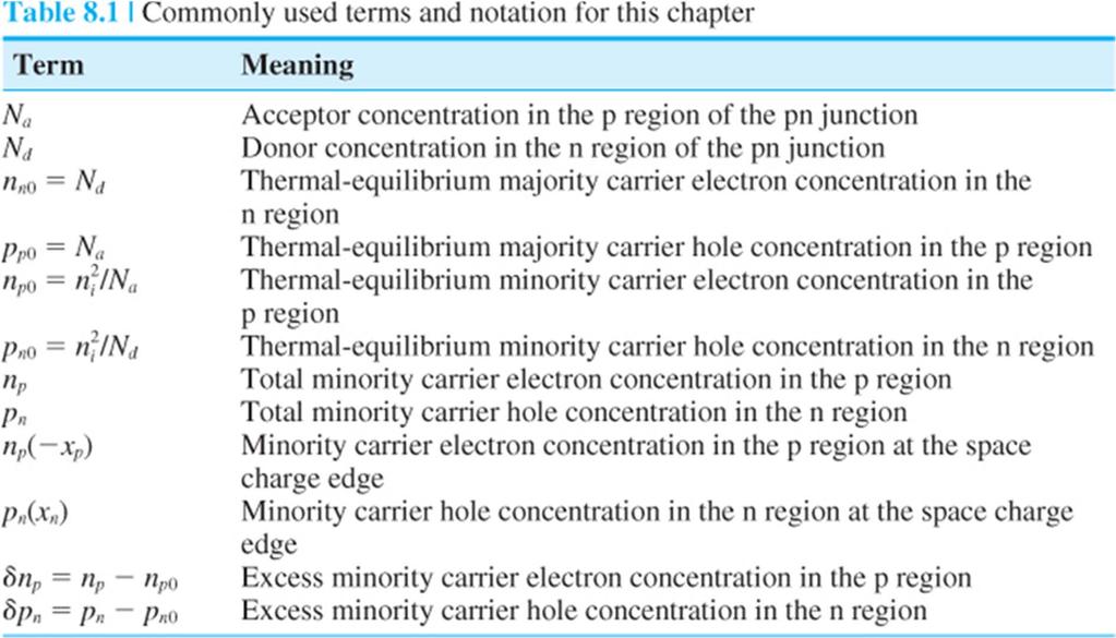
CHAPTER 8 The pn Junction Diode
|
|
|
- Anastasia Atkinson
- 5 years ago
- Views:
Transcription
1 CHAPTER 8 The pn Junction Diode Consider the process by which the potential barrier of a pn junction is lowered when a forward bias voltage is applied, so holes and electrons can flow across the junction generating a diode current. Derive the boundary conditions for excess holes in the n region and excess electrons in the p region, and analyze the behavior of these excess carriers under a forward bias. Derive the ideal current voltage relation of the forward biased pn junction diode. Describe and analyze nonideal effects in the pn junction diode such as high level injection, and generation and recombination currents. Develop a small signal equivalent circuit of the pn junction diode. This equivalent circuit is used to relate small time varying currents and voltages in the pn junction. Discuss large signal diode switching characteristics. Describe a specialized pn junction called a tunnel diode. 1
2 In Figure 8.1c, the total potential barrier is reduced. There will be a diffusion of holes from the p region across the space charge region where they will flow into the n region. Similarly, there will be a diffusion of electrons from the n region across the space charge region where they will flow into the p region. 2

3 The ideal current voltage relationship of a pn junction is derived on the basis of four assumptions. 1. The abrupt depletion layer approximation applies. The space charge regions have abrupt boundaries, and the semiconductor is neutral outside of the depletion region. 2. The Maxwell Boltzmann approximation applies to carrier statistics. 3. The concepts of low injection and complete ionization apply. 4a. The total current is a constant throughout the entire pn structure. 4b. The individual electron and hole currents are continuous functions through the pn structure. 4c. The individual electron and hole currents are constant throughout the depletion region. The built in potential barrier prevents this large density of electrons from flowing into the p region. 3
4 4

5 The electric field Eapp induced by the applied voltage is in the opposite direction to the thermal equilibrium space charge electric field, so the net electric field in the space charge region is reduced below the equilibrium value. The electric field force that prevented majority carriers from crossing the space charge region is reduced; majority carrier electrons from the n side are now injected across the depletion region into the p material, and majority carrier holes from the p side are injected across the depletion region into the n material. 5
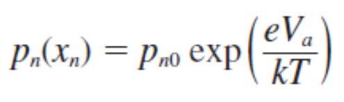
6 Comment of Ex 8.1 The minority carrier concentrations can increase by many orders of magnitude when a relatively small forward bias voltage is applied. 6
7 If a reverse biased voltage greater than a few tenths of a volt is applied to the pn junction, then we see from Equations (8.6) and (8.7) that the minority carrier concentrations at the space charge edge are essentially zero Minority Carrier Distribution 7
8 8
9 The quasi Fermi levels are linear functions of distance in the neutral p and n regions close to the space charge edge in the p region, EFn EFi > 0 which means that δn > ni. Further from the space charge edge, EFn EFi < 0 which means that δn< 9 ni and the excess electron concentration is approaching zero.

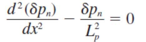
10 8.1.5 Ideal pn Junction Current the total pn junction current will be the minority carrier hole diffusion current at x = xn plus the minority carrier electron diffusion current at x = xp. 10
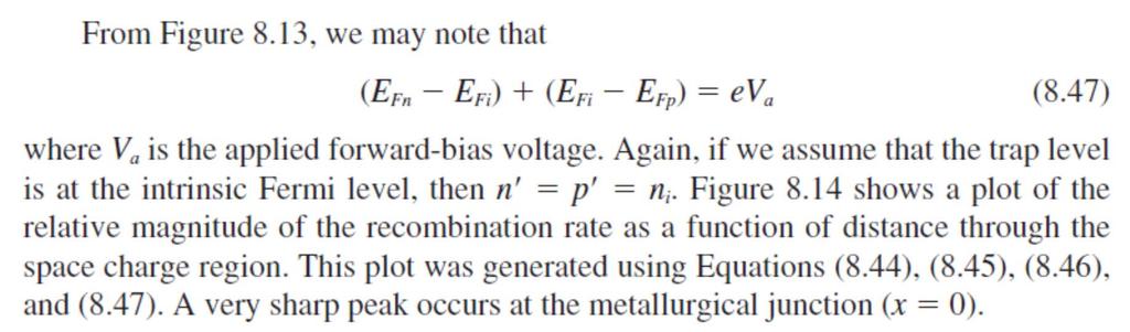
11 11
12 If the voltage Va becomes negative (reverse bias) by a few kt ev, then the reverse biased current density becomes independent of the reverse biased voltage. The parameter Js is then referred to as the reverse saturation current density. 12
13 Comment of Ex 8.2, The ideal reverse biased saturation current density is very small. Ideally, this plot yields a straight line when Va is greater than a few kt ev. The forward bias current is an exponential function of the forwardbias voltage. The difference between total current and minority carrier diffusion current is a majority carrier current. 13
14 Comment of Ex 8.4, We assumed, in the derivation of the current voltage equation, that the electric field in the neutral p and n regions was zero. Although the electric field is not zero, this example shows that the magnitude is very small thus the approximation of zero electric field is very good. 14

15 8.1.7 Temperature Effect For a silicon pn junction, the ideal reverse saturation current density will increase by approximately a factor of 4 for every 10 C increase in temperature. As temperature increases, less forward bias voltage is required to obtain the same diode current. If the voltage is held constant, the diode current will increase as temperature increases The Short Diode the length Wn is assumed to be much smaller than the minority carrier hole diffusion length, Lp. 15
16 16
17 Since the minority carrier concentration is approximately a linear function of distance through the n region, the minority carrier diffusion current density is a constant. 8.2 GENERATION RECOMBINATION CURRENTS AND HIGH INJECTION LEVELS Generation Recombination Currents 17
18 The negative sign implies a negative recombination rate; hence, we are really generating electron hole pairs within the reverse biased space charge region. 18
19 Comment of Ex 8.6, for the silicon pn junction diode at room temperature, the generation current density is approximately four orders of magnitude larger than the ideal saturation current density. The generation current is the dominant reverse biased current in a silicon pn junction diode. 19

20 Forward Bias Recombination Current 20
21 At the center of the space charge region, 21
22 Total Forward Bias Current The total forward bias current density in the pn junction is the sum of the recombination and the ideal diffusion current densities. If some of the injected holes in the space charge region are lost due to recombination, then additional holes must be injected from the p region to make up for this loss. The flow of these additional injected carriers, per unit time, results in the recombination current. 22
23 23
24 8.2.2 High Level Injection 24
25 In the high level injection region, it takes a larger increase in diode voltage to produce a given increase in diode current. 8.3 SMALL SIGNAL MODEL OF THE pn JUNCTION 25
26 If we assume that the diode is biased sufficiently far in the forwardbias region, then the ( 1) term can be neglected and the incremental conductance becomes The incremental resistance is also known as the diffusion resistance. 26
27 The shaded areas represents the charge Q that is alternately charged and discharged during the ac voltage cycle. The mechanism of charging and discharging of holes in the n region and electrons in the p region leads to a capacitance, called diffusion capacitance. the magnitude of the diffusion capacitance in a forward biased pn junction 27is usually substantially larger than the junction capacitance.
28 Mathematical Analysis assume 1v1(t)1 <(kt/ e) = Vt, the time-varying voltage v1(t) isa sinusoidal signal, 28
29 dc ac 29
30 One consequence of the approximations ωtp0 < 1 and ωtn0 < 1 is that there are no wiggles in the minority carrier curves. The sinusoidal frequency is low enough so that the exponential curves are maintained at all times. 30
31 8.3.3 Equivalent Circuit 31
32 *8.4 CHARGE STORAGE AND DIODE TRANSIENTS 32
33 the reverse biased density gradient is constant; thus, the minority carrier concentrations at the space charge edge decrease with time This reverse current IR will be approximately constant for 0< t< ts, where ts is called the storage time. 33
34 *8.5 THE TUNNEL DIODE The tunnel diode is a pn junction in which both the n and p regions are degenerately doped. The depletion region width decreases as the doping increases and may be on the order of approximately 100 Å 34
35 (b) There is a finite probability that some of these electrons will tunnel directly into the empty states, producing a forward bias tunneling current (e) the tunneling current will be zero and the normal ideal diffusion current will exist 35
36 Electrons in the valence band on the p side are directly opposite empty states in the conduction band on the n side, so electrons can now tunnel directly from the p region into the n region, resulting in a large reversebiased tunneling current. 36
CHAPTER 8 The PN Junction Diode
 CHAPTER 8 The PN Junction Diode Consider the process by which the potential barrier of a PN junction is lowered when a forward bias voltage is applied, so holes and electrons can flow across the junction
CHAPTER 8 The PN Junction Diode
 CHAPTER 8 The PN Junction Diode Consider the process by which the potential barrier of a PN junction is lowered when a forward bias voltage is applied, so holes and electrons can flow across the junction
Lecture 2 p-n junction Diode characteristics. By Asst. Prof Dr. Jassim K. Hmood
 Electronic I Lecture 2 p-n junction Diode characteristics By Asst. Prof Dr. Jassim K. Hmood THE p-n JUNCTION DIODE The pn junction diode is formed by fabrication of a p-type semiconductor region in intimate
Semiconductor Devices Lecture 5, pn-junction Diode
 Semiconductor Devices Lecture 5, pn-junction Diode Content Contact potential Space charge region, Electric Field, depletion depth Current-Voltage characteristic Depletion layer capacitance Diffusion capacitance
Digital Integrated Circuits A Design Perspective. The Devices. Digital Integrated Circuits 2nd Devices
 Digital Integrated Circuits A Design Perspective The Devices The Diode The diodes are rarely explicitly used in modern integrated circuits However, a MOS transistor contains at least two reverse biased
Review Energy Bands Carrier Density & Mobility Carrier Transport Generation and Recombination
 Review Energy Bands Carrier Density & Mobility Carrier Transport Generation and Recombination Current Transport: Diffusion, Thermionic Emission & Tunneling For Diffusion current, the depletion layer is
EC T34 ELECTRONIC DEVICES AND CIRCUITS
 RAJIV GANDHI COLLEGE OF ENGINEERING AND TECHNOLOGY PONDY-CUDDALORE MAIN ROAD, KIRUMAMPAKKAM-PUDUCHERRY DEPARTMENT OF ECE EC T34 ELECTRONIC DEVICES AND CIRCUITS II YEAR Mr.L.ARUNJEEVA., AP/ECE 1 PN JUNCTION
R. W. Erickson. Department of Electrical, Computer, and Energy Engineering University of Colorado, Boulder
 R. W. Erickson Department of Electrical, Computer, and Energy Engineering University of Colorado, Boulder pn junction! Junction diode consisting of! p-doped silicon! n-doped silicon! A p-n junction where
EE/COE 152: Basic Electronics. Lecture 3. A.S Agbemenu. https://sites.google.com/site/agbemenu/courses/ee-coe-152
 EE/COE 152: Basic Electronics Lecture 3 A.S Agbemenu https://sites.google.com/site/agbemenu/courses/ee-coe-152 Books: Microelcetronic Circuit Design (Jaeger/Blalock) Microelectronic Circuits (Sedra/Smith)
ECE 440 Lecture 29 : Introduction to the BJT-I Class Outline:
 ECE 440 Lecture 29 : Introduction to the BJT-I Class Outline: Narrow-Base Diode BJT Fundamentals BJT Amplification Things you should know when you leave Key Questions How does the narrow-base diode multiply
NAME: Last First Signature
 UNIVERSITY OF CALIFORNIA, BERKELEY College of Engineering Department of Electrical Engineering and Computer Sciences EE 130: IC Devices Spring 2003 FINAL EXAMINATION NAME: Last First Signature STUDENT
semiconductor p-n junction Potential difference across the depletion region is called the built-in potential barrier, or built-in voltage:
 Chapter four The Equilibrium pn Junction The Electric field will create a force that will stop the diffusion of carriers reaches thermal equilibrium condition Potential difference across the depletion
Physics 160 Lecture 5. R. Johnson April 13, 2015
 Physics 160 Lecture 5 R. Johnson April 13, 2015 Half Wave Diode Rectifiers Full Wave April 13, 2015 Physics 160 2 Note that there is no ground connection on this side of the rectifier! Output Smoothing
Laboratory No. 01: Small & Large Signal Diode Circuits. Electrical Enginnering Departement. By: Dr. Awad Al-Zaben. Instructor: Eng.
 Laboratory No. 01: Small & Large Signal Diode Circuits Electrical Enginnering Departement By: Dr. Awad Al-Zaben Instructor: Eng. Tamer Shahta Electronics Laboratory EE 3191 February 23, 2014 I. OBJECTIVES
Chapter 2 PN junction and diodes
 Chapter 2 PN junction and diodes ELEC-H402/CH2: PN junction and diodes 1 PN junction and diodes PN junction What happens in a PN junction Currents through the PN junction Properties of the depletion region
Department of Electrical Engineering IIT Madras
 Department of Electrical Engineering IIT Madras Sample Questions on Semiconductor Devices EE3 applicants who are interested to pursue their research in microelectronics devices area (fabrication and/or
PN Junction in equilibrium
 PN Junction in equilibrium PN junctions are important for the following reasons: (i) PN junction is an important semiconductor device in itself and used in a wide variety of applications such as rectifiers,
Bipolar Junction Transistors (BJTs) Overview
 Overview") 1 Bipolar Junction Transistors (BJTs) Asst. Prof. MONTREE SIRIPRUCHYANUN, D. Eng. Dept. of Teacher Training in Electrical Engineering, Faculty of Technical Education King Mongkut s Institute of Technology
1 Bipolar Junction Transistors (BJTs) Asst. Prof. MONTREE SIRIPRUCHYANUN, D. Eng. Dept. of Teacher Training in Electrical Engineering, Faculty of Technical Education King Mongkut s Institute of Technology
Section 2.3 Bipolar junction transistors - BJTs
 Section 2.3 Bipolar junction transistors - BJTs Single junction devices, such as p-n and Schottkty diodes can be used to obtain rectifying I-V characteristics, and to form electronic switching circuits
Ch5 Diodes and Diodes Circuits
 Circuits and Analog Electronics Ch5 Diodes and Diodes Circuits 5.1 The Physical Principles of Semiconductor 5.2 Diodes 5.3 Diode Circuits 5.4 Zener Diode References: Floyd-Ch2; Gao-Ch6; 5.1 The Physical
What is the highest efficiency Solar Cell?
 What is the highest efficiency Solar Cell? GT CRC Roof-Mounted PV System Largest single PV structure at the time of it s construction for the 1996 Olympic games Produced more than 1 billion watt hrs. of
Semiconductor Physics and Devices
 Metal-Semiconductor and Semiconductor Heterojunctions The Metal-Oxide-Semiconductor Field-Effect Transistor (MOSFET) is one of two major types of transistors. The MOSFET is used in digital circuit, because
EE70 - Intro. Electronics
 EE70 - Intro. Electronics Course website: ~/classes/ee70/fall05 Today s class agenda (November 28, 2005) review Serial/parallel resonant circuits Diode Field Effect Transistor (FET) f 0 = Qs = Qs = 1 2π
Intrinsic Semiconductor
 Semiconductors Crystalline solid materials whose resistivities are values between those of conductors and insulators. Good electrical characteristics and feasible fabrication technology are some reasons
Microelectronic Circuits, Kyung Hee Univ. Spring, Bipolar Junction Transistors
 Bipolar Junction Transistors 1 Introduction physical structure of the bipolar transistor and how it works How the voltage between two terminals of the transistor controls the current that flows through
ELEC 3908, Physical Electronics, Lecture 16. Bipolar Transistor Operation
 ELEC 3908, Physical Electronics, Lecture 16 Bipolar Transistor Operation Lecture Outline Last lecture discussed the structure and fabrication of a double diffused bipolar transistor Now examine current
CONTENTS. 2.2 Schrodinger's Wave Equation 31. PART I Semiconductor Material Properties. 2.3 Applications of Schrodinger's Wave Equation 34
 CONTENTS Preface x Prologue Semiconductors and the Integrated Circuit xvii PART I Semiconductor Material Properties CHAPTER 1 The Crystal Structure of Solids 1 1.0 Preview 1 1.1 Semiconductor Materials
Unless otherwise specified, assume room temperature (T = 300 K).
.") ECE 3040 Dr. Doolittle Homework 4 Unless otherwise specified, assume room temperature (T = 300 K). 1) Purpose: Understanding p-n junction band diagrams. Consider a p-n junction with N A = 5x10 14 cm -3
ECE 3040 Dr. Doolittle Homework 4 Unless otherwise specified, assume room temperature (T = 300 K). 1) Purpose: Understanding p-n junction band diagrams. Consider a p-n junction with N A = 5x10 14 cm -3
EDC Lecture Notes UNIT-1
 P-N Junction Diode EDC Lecture Notes Diode: A pure silicon crystal or germanium crystal is known as an intrinsic semiconductor. There are not enough free electrons and holes in an intrinsic semi-conductor
Analog Electronic Circuits
 Analog Electronic Circuits Chapter 1: Semiconductor Diodes Objectives: To become familiar with the working principles of semiconductor diode To become familiar with the design and analysis of diode circuits
Lecture 7:PN Junction. Structure, Depletion region, Different bias Conditions, IV characteristics, Examples
 Lecture 7:PN Junction Structure, Depletion region, Different bias Conditions, IV characteristics, Examples PN Junction The diode (pn junction) is formed by dopping a piece of intrinsic silicon, such that
Downloaded from
 Question 14.1: In an n-type silicon, which of the following statement is true: (a) Electrons are majority carriers and trivalent atoms are the dopants. (b) Electrons are minority carriers and pentavalent
10/27/2009 Reading: Chapter 10 of Hambley Basic Device Physics Handout (optional)
") EE40 Lec 17 PN Junctions Prof. Nathan Cheung 10/27/2009 Reading: Chapter 10 of Hambley Basic Device Physics Handout (optional) Slide 1 PN Junctions Semiconductor Physics of pn junctions (for reference
EE40 Lec 17 PN Junctions Prof. Nathan Cheung 10/27/2009 Reading: Chapter 10 of Hambley Basic Device Physics Handout (optional) Slide 1 PN Junctions Semiconductor Physics of pn junctions (for reference
UNIT 3: FIELD EFFECT TRANSISTORS
 FIELD EFFECT TRANSISTOR: UNIT 3: FIELD EFFECT TRANSISTORS The field effect transistor is a semiconductor device, which depends for its operation on the control of current by an electric field. There are
Electronics I. Midterm #1
 EECS:3400 Electronics I s5ms_elct7.fm - Section Electronics I Midterm # Problems Points. 4 2. 5 3. 6 Total 5 Was the exam fair? yes no EECS:3400 Electronics I s5ms_elct7.fm - 2 Problem 4 points For full
Semiconductor Materials and Diodes
 C C H H A A P P T T E E R R 1 Semiconductor Materials and Diodes 1.0 1.0 PREVIEW PREVIEW This text deals with the analysis and design of circuits containing electronic devices, such as diodes and transistors.
R. W. Erickson. Department of Electrical, Computer, and Energy Engineering University of Colorado, Boulder
 R. W. Erickson Department of Electrical, Computer, and Energy Engineering University of Colorado, Boulder Inclusion of Switching Loss in the Averaged Equivalent Circuit Model The methods of Chapter 3 can
Electronics I. Midterm #1
 The University of Toledo s6ms_elct7.fm - Electronics I Midterm # Problems Points. 4 2. 5 3. 6 Total 5 Was the exam fair? yes no The University of Toledo s6ms_elct7.fm - 2 Problem 4 points For full credit,
KOM2751 Analog Electronics :: Dr. Muharrem Mercimek :: YTU - Control and Automation Dept. 1 1 (CONT D) DIODES
 DIODES") KOM2751 Analog Electronics :: Dr. Muharrem Mercimek :: YTU - Control and Automation Dept. 1 1 (CONT D) DIODES Most of the content is from the textbook: Electronic devices and circuit theory, Robert L.
KOM2751 Analog Electronics :: Dr. Muharrem Mercimek :: YTU - Control and Automation Dept. 1 1 (CONT D) DIODES Most of the content is from the textbook: Electronic devices and circuit theory, Robert L.
ECE 340 Lecture 29 : LEDs and Lasers Class Outline:
 ECE 340 Lecture 29 : LEDs and Lasers Class Outline: Light Emitting Diodes Lasers Semiconductor Lasers Things you should know when you leave Key Questions What is an LED and how does it work? How does a
Electronics I. Midterm #1
 The University of Toledo Section f6ms_elct7.fm - Electronics I Midterm # Problems Points. 4 2. 5 3. 6 Total 5 Was the exam fair? yes no The University of Toledo f6ms_elct7.fm - 2 Problem 4 points For full
Chapter 1: Semiconductor Diodes
 Chapter 1: Semiconductor Diodes Diodes The diode is a 2-terminal device. A diode ideally conducts in only one direction. 2 Diode Characteristics Conduction Region Non-Conduction Region The voltage across
Key Questions. What is an LED and how does it work? How does a laser work? How does a semiconductor laser work? ECE 340 Lecture 29 : LEDs and Lasers
 Things you should know when you leave Key Questions ECE 340 Lecture 29 : LEDs and Class Outline: What is an LED and how does it How does a laser How does a semiconductor laser How do light emitting diodes
Lecture 4. Reading: Chapter EE105 Fall 2007 Lecture 4, Slide 1 Prof. Liu, UC Berkeley
 Lecture 4 OUTLNE Bipolar Junction Transistor (BJT) General considerations Structure Operation in active mode Large-signal model and - characteristics Reading: Chapter 4.1-4.4.2 EE105 Fall 2007 Lecture
(Refer Slide Time: 01:33)
") Solid State Devices Dr. S. Karmalkar Department of Electronics and Communication Engineering Indian Institute of Technology, Madras Lecture - 31 Bipolar Junction Transistor (Contd ) So, we have been discussing
Solid State Devices Dr. S. Karmalkar Department of Electronics and Communication Engineering Indian Institute of Technology, Madras Lecture - 31 Bipolar Junction Transistor (Contd ) So, we have been discussing
Alexandria University Faculty of Engineering Electrical Engineering Department
 Chapter 10: Alexandria University Faculty of Engineering Electrical Engineering Department ECE 336: Semiconductor Devices Sheet 6 1. A Si pnp BJT with N AE = 5x10 17 / cm 3, N DB = 10 15 /cm 3 and N AC
Lecture -1: p-n Junction Diode
 Lecture -1: p-n Junction Diode Diode: A pure silicon crystal or germanium crystal is known as an intrinsic semiconductor. There are not enough free electrons and holes in an intrinsic semi-conductor to
Part II. Devices Diode, BJT, MOSFETs
 Part II Devices Diode, BJT, MOSFETs 49 4 Semiconductor Semiconductor The number of charge carriers available to conduct current 1 is between that of conductors and that of insulators. Semiconductor is
Electron Devices and Circuits (EC 8353)
") Electron Devices and Circuits (EC 8353) Prepared by Ms.S.KARKUZHALI, A.P/EEE Diodes The diode is a 2-terminal device. A diode ideally conducts in only one direction. Diode Characteristics Conduction Region
Electron Devices and Circuits (EC 8353) Prepared by Ms.S.KARKUZHALI, A.P/EEE Diodes The diode is a 2-terminal device. A diode ideally conducts in only one direction. Diode Characteristics Conduction Region
Lecture 9: Limiting and Clamping Diode Circuits. Voltage Doubler. Special Diode Types.
 Whites, EE 320 Lecture 9 Page 1 of 8 Lecture 9: Limiting and Clamping Diode Circuits. Voltage Doubler. Special Diode Types. We ll finish up our discussion of diodes in this lecture by consider a few more
Lecture 3: Diodes. Amplitude Modulation. Diode Detection.
 Whites, EE 322 Lecture 3 Page 1 of 10 Lecture 3: Diodes. Amplitude Modulation. Diode Detection. Diodes are the fourth basic discrete component listed in Lecture 2. These and transistors are both nonlinear
Simulation of MOSFETs, BJTs and JFETs. At and Near the Pinch-off Region. Xuan Yang
 Simulation of MOSFETs, BJTs and JFETs At and Near the Pinch-off Region by Xuan Yang A Thesis Presented in Partial Fulfillment of the Requirements for the Degree Master of Science Approved November 2011
Lecture 4. pn Junctions (Diodes) Wednesday 27/9/2017 pn junctions 1-1
 Wednesday 27/9/2017 pn junctions 1-1") Lecture 4 n Junctions (Diodes) Wednesday 27/9/2017 n junctions 1-1 Agenda Continue n junctions Equilibrium (zero bias) Deletion rejoins Built-in otential Reverse and forward bias I-V characteristics Bias
Lecture 4 n Junctions (Diodes) Wednesday 27/9/2017 n junctions 1-1 Agenda Continue n junctions Equilibrium (zero bias) Deletion rejoins Built-in otential Reverse and forward bias I-V characteristics Bias
Lesson 5. Electronics: Semiconductors Doping p-n Junction Diode Half Wave and Full Wave Rectification Introduction to Transistors-
 Lesson 5 Electronics: Semiconductors Doping p-n Junction Diode Half Wave and Full Wave Rectification Introduction to Transistors- Types and Connections Semiconductors Semiconductors If there are many free
Electronics The basics of semiconductor physics
 Electronics The basics of semiconductor physics Prof. Márta Rencz, Gábor Takács BME DED 17/09/2015 1 / 37 The basic properties of semiconductors Range of conductivity [Source: http://www.britannica.com]
BJT. Bipolar Junction Transistor BJT BJT 11/6/2018. Dr. Satish Chandra, Assistant Professor, P P N College, Kanpur 1
 BJT Bipolar Junction Transistor Satish Chandra Assistant Professor Department of Physics P P N College, Kanpur www.satish0402.weebly.com The Bipolar Junction Transistor is a semiconductor device which
COE/EE152: Basic Electronics. Lecture 5. Andrew Selasi Agbemenu. Outline
 COE/EE152: Basic Electronics Lecture 5 Andrew Selasi Agbemenu 1 Outline Physical Structure of BJT Two Diode Analogy Modes of Operation Forward Active Mode of BJTs BJT Configurations Early Effect Large
THERMIONIC AND GASEOUS STATE DIODES
 THERMIONIC AND GASEOUS STATE DIODES Thermionic and gaseous state (vacuum tube) diodes Thermionic diodes are thermionic-valve devices (also known as vacuum tubes, tubes, or valves), which are arrangements
Key Questions. ECE 340 Lecture 39 : Introduction to the BJT-II 4/28/14. Class Outline: Fabrication of BJTs BJT Operation
 Things you should know when you leave ECE 340 Lecture 39 : Introduction to the BJT-II Fabrication of BJTs Class Outline: Key Questions What elements make up the base current? What do the carrier distributions
Structure of Actual Transistors
 4.1.3. Structure of Actual Transistors Figure 4.7 shows a more realistic BJT cross-section Collector virtually surrounds entire emitter region This makes it difficult for electrons injected into base to
PROLOGUE TO ELECTRONICS
 PROLOGUE TO ELECTRONICS When most of us hear the word electronics, we think of televisions, laptop computers, cell phones, or ipods. Actually, these items are electronic systems composed of subsystems
Basic Electronics Prof. Dr. Chitralekha Mahanta Department of Electronics and Communication Engineering Indian Institute of Technology, Guwahati
 Basic Electronics Prof. Dr. Chitralekha Mahanta Department of Electronics and Communication Engineering Indian Institute of Technology, Guwahati Module: 2 Bipolar Junction Transistors Lecture-1 Transistor
Electronic devices-i. Difference between conductors, insulators and semiconductors
 Electronic devices-i Semiconductor Devices is one of the important and easy units in class XII CBSE Physics syllabus. It is easy to understand and learn. Generally the questions asked are simple. The unit
The shape of the waveform will be the same, but its level is shifted either upward or downward. The values of the resistor R and capacitor C affect
 Diode as Clamper A clamping circuit is used to place either the positive or negative peak of a signal at a desired level. The dc component is simply added or subtracted to/from the input signal. The clamper
Diodes and Applications
 Diodes and Applications Diodes and Applications 2 1 Diode Operation 2 2 Voltage-Current (V-I) Characteristics 2 3 Diode Models 2 4 Half-Wave Rectifiers 2 5 Full-Wave Rectifiers 2 6 Power Supply Filters
Analog Electronics (Course Code: EE314) Lecture 5 7: Junction contd, BJT. Course Instructor: Shree Prakash Tiwari
 Lecture 5 7: Junction contd, BJT. Course Instructor: Shree Prakash Tiwari") ndian nstitute of echnology Jodhpur, Year 2017 Analog lectronics (ourse ode: 314) Lecture 5 7: Junction contd, J ourse nstructor: Shree Prakash iwari mail: sptiwari@iitj.ac.in Webpage: http://home.iitj.ac.in/~sptiwari/
ndian nstitute of echnology Jodhpur, Year 2017 Analog lectronics (ourse ode: 314) Lecture 5 7: Junction contd, J ourse nstructor: Shree Prakash iwari mail: sptiwari@iitj.ac.in Webpage: http://home.iitj.ac.in/~sptiwari/
Electronic Circuits I - Tutorial 03 Diode Applications I
 Electronic Circuits I - Tutorial 03 Diode Applications I -1 / 13 - T & F # Question 1 A diode can conduct current in two directions with equal ease. F 2 When reverse-biased, a diode ideally appears as
ES 330 Electronics II Homework # 1 (Fall 2016 SOLUTIONS)
") SOLUTIONS ES 330 Electronics II Homework # 1 (Fall 2016 SOLUTIONS) Problem 1 (20 points) We know that a pn junction diode has an exponential I-V behavior when forward biased. The diode equation relating
SOLUTIONS ES 330 Electronics II Homework # 1 (Fall 2016 SOLUTIONS) Problem 1 (20 points) We know that a pn junction diode has an exponential I-V behavior when forward biased. The diode equation relating
Sub-Threshold Region Behavior of Long Channel MOSFET
 Sub-threshold Region - So far, we have discussed the MOSFET behavior in linear region and saturation region - Sub-threshold region is refer to region where Vt is less than Vt - Sub-threshold region reflects
PHYSICS OF SEMICONDUCTOR DEVICES
 PHYSICS OF SEMICONDUCTOR DEVICES PHYSICS OF SEMICONDUCTOR DEVICES by J. P. Colinge Department of Electrical and Computer Engineering University of California, Davis C. A. Colinge Department of Electrical
Università degli Studi di Roma Tor Vergata Dipartimento di Ingegneria Elettronica. Analogue Electronics. Paolo Colantonio A.A.
 Università degli Studi di Roma Tor Vergata Dipartimento di Ingegneria Elettronica Analogue Electronics Paolo Colantonio A.A. 2015-16 Introduction: materials Conductors e.g. copper or aluminum have a cloud
15 Transit Time and Tunnel NDR Devices
 15 Transit Time and Tunnel NDR Devices Schematics of Transit-time NDR diode. A packet of carriers (e.g., electrons) is generated in a confined and narrow zone (generation region) and injected into the
ECE 3040 Dr. Alan Doolittle.
 ECE 3040 Dr. Alan Doolittle I have thoroughly enjoyed meeting each of you and hope that I have had a positive influence on your carriers. Please feel free to consult with me in your future work. If I can
EXPERIMENT 10: SCHOTTKY DIODE CHARACTERISTICS
 EXPERIMENT 10: SCHOTTKY DIODE CHARACTERISTICS AIM: To plot forward and reverse characteristics of Schottky diode (Metal Semiconductor junction) APPARATUS: D.C. Supply (0 15 V), current limiting resistor
EC6202- ELECTRONIC DEVICES AND CIRCUITS UNIT TEST-1 EXPECTED QUESTIONS
 EC6202- ELECTRONIC DEVICES AND CIRCUITS UNIT TEST-1 EXPECTED QUESTIONS 1. List the PN diode parameters. 1. Bulk Resistance. 2. Static Resistance/Junction Resistance (or) DC Forward Resistance 3. Dynamic
 Electronic Devices 1. Current flowing in each of the following circuits A and respectively are: (Circuit 1) (Circuit 2) 1) 1A, 2A 2) 2A, 1A 3) 4A, 2A 4) 2A, 4A 2. Among the following one statement is not
Chapter 2. Diodes & Applications
 Chapter 2 Diodes & Applications The Diode A diode is made from a small piece of semiconductor material, usually silicon, in which half is doped as a p region and half is doped as an n region with a pn
IENGINEERS- CONSULTANTS LECTURE NOTES SERIES ELECTRONICS ENGINEERING 1 YEAR UPTU. Lecture-4
 2 P-n Lecture-4 20 Introduction: If a junction is formed between a p-type and a n-type semiconductor this combination is known as p-n junction diode and has the properties of a rectifier 21 Formation of
UNIT 3 Transistors JFET
 UNIT 3 Transistors JFET Mosfet Definition of BJT A bipolar junction transistor is a three terminal semiconductor device consisting of two p-n junctions which is able to amplify or magnify a signal. It
exp T ln exp Excercise 1: Semiconductors / pn-junctions Carrier concentrations
 Excercise 1: emiconductors / n-junctions Carrier concentrations 1. Consider undoed GaAs (N c=4.7x10 17 cm -3, N v=7.0x10 18 cm -3, E g=1.424 ev) and i (N c=2.8x10 19 cm -3, N v=1.04x10 19, cm -3, E g=1.12
Project 6 Capacitance of a PN Junction Diode
 Project 6 Capacitance of a PN Junction Diode OVERVIEW: In this project, we will characterize the capacitance of a reverse-biased PN diode. We will see that this capacitance is voltage-dependent and we
Analog & Digital Electronics Course No: PH-218
 Analog & Digital Electronics Course No: PH-218 Lec-5: Bipolar Junction Transistor (BJT) Course nstructors: Dr. A. P. VAJPEY Department of Physics, ndian nstitute of Technology Guwahati, ndia 1 Bipolar
Solid State Devices- Part- II. Module- IV
 Solid State Devices- Part- II Module- IV MOS Capacitor Two terminal MOS device MOS = Metal- Oxide- Semiconductor MOS capacitor - the heart of the MOSFET The MOS capacitor is used to induce charge at the
Semiconductor Devices
 Semiconductor Devices Modelling and Technology Source Electrons Gate Holes Drain Insulator Nandita DasGupta Amitava DasGupta SEMICONDUCTOR DEVICES Modelling and Technology NANDITA DASGUPTA Professor Department
Lecture-45. MOS Field-Effect-Transistors Threshold voltage
 Lecture-45 MOS Field-Effect-Transistors 7.4. Threshold voltage In this section we summarize the calculation of the threshold voltage and discuss the dependence of the threshold voltage on the bias applied
Chapter 8. Field Effect Transistor
 Chapter 8. Field Effect Transistor Field Effect Transistor: The field effect transistor is a semiconductor device, which depends for its operation on the control of current by an electric field. There
CHAPTER 1 DIODE CIRCUITS. Semiconductor act differently to DC and AC currents
 CHAPTER 1 DIODE CIRCUITS Resistance levels Semiconductor act differently to DC and AC currents There are three types of resistances 1. DC or static resistance The application of DC voltage to a circuit
PN Junction Diode Table of Contents. What Are Diodes Made Out Of?
 PN Junction iode Table of Contents What are diodes made out of?slide 3 N-type materialslide 4 P-type materialslide 5 The pn junctionslides 6-7 The biased pn junctionslides 8-9 Properties of diodesslides
(Refer Slide Time: 05:47)
") Solid State Devices Dr. S. Karmalkar Department of Electronics and Communication Engineering Indian Institute of Technology, Madras Lecture - 29 Bipolar Junction Transistor (Contd ) So we have been discussing
Solid State Devices Dr. S. Karmalkar Department of Electronics and Communication Engineering Indian Institute of Technology, Madras Lecture - 29 Bipolar Junction Transistor (Contd ) So we have been discussing
Discuss the basic structure of atoms Discuss properties of insulators, conductors, and semiconductors
 Discuss the basic structure of atoms Discuss properties of insulators, conductors, and semiconductors Discuss covalent bonding Describe the properties of both p and n type materials Discuss both forward
EJERCICIOS DE COMPONENTES ELECTRÓNICOS. 1 er cuatrimestre
 EJECICIOS DE COMPONENTES ELECTÓNICOS. 1 er cuatrimestre 2 o Ingeniería Electrónica Industrial Juan Antonio Jiménez Tejada Índice 1. Basic concepts of Electronics 1 2. Passive components 1 3. Semiconductors.
Electronics Review Flashcards
 November 21, 2011 1 Op Amps 2 Diodes 3 Silicon 4 pn Junctions 5 BJTs 6 MOSFETs Open Loop Characteristics Open-Loop Op-Amp Characteristics (first-order model) Closed Loop Characteristics Closed-Loop Op-Amp
The Semiconductor Diode
 Physics Topics The Semiconductor Diode If necessary, review the following topics and relevant textbook sections from Neamen Semiconductor Physics and Devices, 4th Ed. Section 8.1.5, especially equation
ECE520 VLSI Design. Lecture 2: Basic MOS Physics. Payman Zarkesh-Ha
 ECE520 VLSI Design Lecture 2: Basic MOS Physics Payman Zarkesh-Ha Office: ECE Bldg. 230B Office hours: Wednesday 2:00-3:00PM or by appointment E-mail: pzarkesh@unm.edu Slide: 1 Review of Last Lecture Semiconductor
Lecture - 18 Transistors
 Electronic Materials, Devices and Fabrication Dr. S. Prarasuraman Department of Metallurgical and Materials Engineering Indian Institute of Technology, Madras Lecture - 18 Transistors Last couple of classes
Reg. No. : Question Paper Code : B.E./B.Tech. DEGREE EXAMINATION, NOVEMBER/DECEMBER Second Semester
 WK 5 Reg. No. : Question Paper Code : 27184 B.E./B.Tech. DEGREE EXAMINATION, NOVEMBER/DECEMBER 2015. Time : Three hours Second Semester Electronics and Communication Engineering EC 6201 ELECTRONIC DEVICES
LAB IV. SILICON DIODE CHARACTERISTICS
 LAB IV. SILICON DIODE CHARACTERISTICS 1. OBJECTIVE In this lab you will measure the I-V characteristics of the rectifier and Zener diodes, in both forward and reverse-bias mode, as well as learn what mechanisms
IENGINEERS- CONSULTANTS QUESTION BANK SERIES ELECTRONICS ENGINEERING 1 YEAR UPTU
 ELECTRONICS ENGINEERING Unit 1 Objectives Q.1 The breakdown mechanism in a lightly doped p-n junction under reverse biased condition is called. (A) avalanche breakdown. (B) zener breakdown. (C) breakdown
Electronic Circuits I. Instructor: Dr. Alaa Mahmoud
 Electronic Circuits I Instructor: Dr. Alaa Mahmoud alaa_y_emam@hotmail.com Chapter 27 Diode and diode application Outline: Semiconductor Materials The P-N Junction Diode Biasing P-N Junction Volt-Ampere
LAB V. LIGHT EMITTING DIODES
 LAB V. LIGHT EMITTING DIODES 1. OBJECTIVE In this lab you are to measure I-V characteristics of Infrared (IR), Red and Blue light emitting diodes (LEDs). The emission intensity as a function of the diode