Scanning Microwave. Expanding Impedance Measurements to the Nanoscale: Coupling the Power of Scanning Probe Microscopy with the PNA
|
|
|
- Edward Parrish
- 5 years ago
- Views:
Transcription

1 Agilent Technologies Scanning Microwave Microscopy (SMM) Expanding Impedance Measurements to the Nanoscale: Coupling the Power of Scanning Probe Microscopy with the PNA Presented by: Craig Wall PhD Product Manager Agilent AFM, Nanomeasurements Division
2 Outline Introduction Principle Instrument setup Experiments Summary Page 2
3 Introduction Available SPM-based techniques to probe materials electric properties: Scanning near-field microwave microscopy (SNMM) Scanning capacitance microscopy (SCM) Scanning spreading resistance microscopy (SSRM) Electrostatic force microscopy (EFM) Current-sensing (or conductive) AFM (CSAFM) Kelvin force microscopy (KFM) More Scanning Probe Microscopy, edited by S. Kalinin and A. Gruverman, Springer, New York, Vector network analyzer + AFM impedance capacitance dopant density more (SMM) Page 3
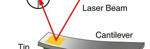
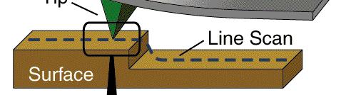
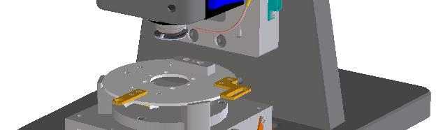
4 AFM Basic Configuration Z Y X AFM tip monitors surface Closed loop scanner (xyz) or stage Scan with tip or with sample Video access Page 4
5 AFM Imaging Modes Contact Mode AFM (1986) Dynamic in x and y Tip is in contact or near contact with the surface Small vertical force, but the probe dragged over the surface exerting lateral force. Weakly bound or soft samples move easily. Lower lateral resolution. AC Mode AFM (1993) Dynamic in x, y, and z Intermittent contact. Soft surfaces are stiffened by viscoelastic response. Impact is predominately vertical, therefore large vertical force, but no lateral force. Higher lateral resolution. Page 5


6 incident Principle transmitted complex reflection coefficient Γ = Z Z L L + Z Z REFLECTION 0 0 reflected Optical analogy incident Reflected Incident = A R SWR S-Parameters Return Loss Impedance, S 11, S 22 Reflection Admittance Coefficient R+jX, Γ, ρ G+jB transmitted reflected Microwave transmission Page 6


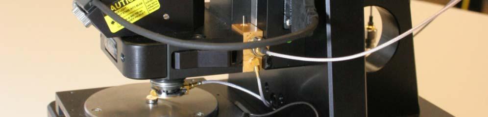
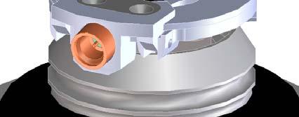
7 Schematic Source Half wave length Coaxial resonator 50 Ohm Probe Page 7


8 Instrument setup AFM professional network analyzer For dc/dv measurements, a low-frequency modulation is added to the microwave. Demodulated signal is detected by an ac mode controller with built-in digital lock-in amplifiers. Page 8


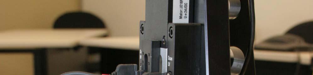
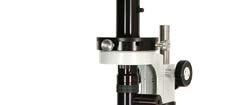
9 Agilent 5400 Based SMM Page 9


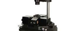
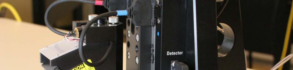
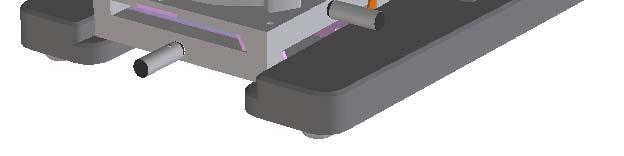
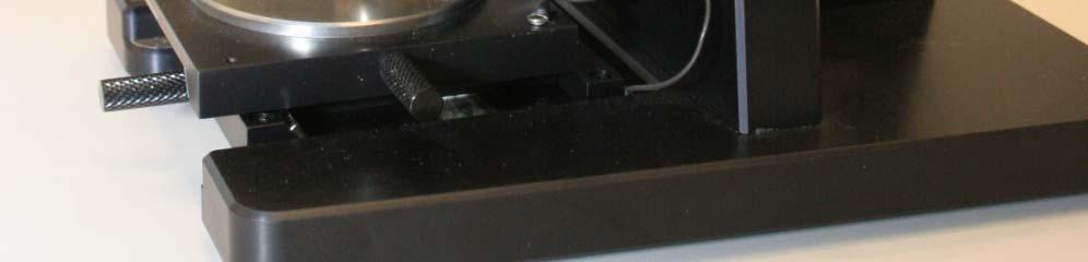
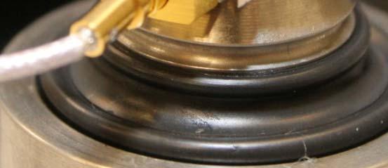
10 Agilent 5400 Based SMM Load Diplexer RF to PNA Scanner head With Conductive Tip Page 10

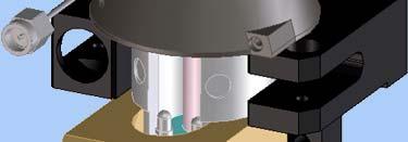
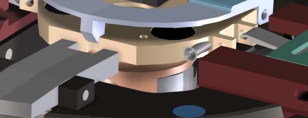
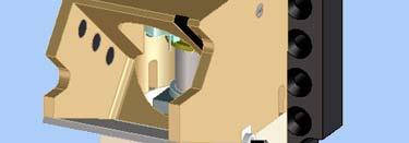
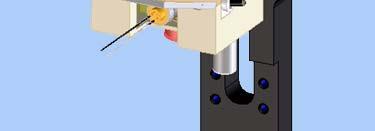

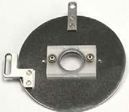
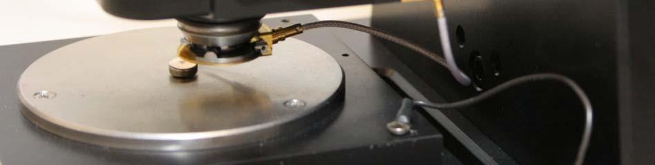
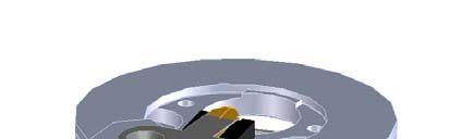
11 Scanner assembly, cantilever Cantilever holder Pt/Ir cantilever Scanner assembly Al substrate Page 11


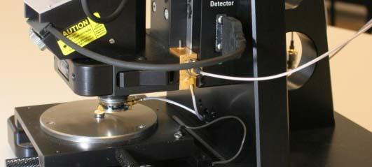
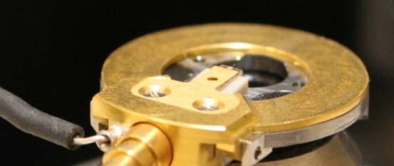
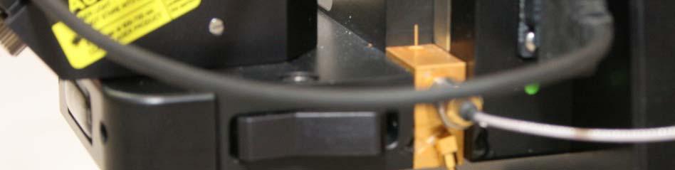
12 Agilent Performance Vector Network Analyzer PNA Signal Conditioning Conductive tip Agilent 5400 SPM Instrument Agilent Precision Machining and Process Technologies to deliver RF/MW to the conductive tip Page 12

13 PNA Controls from PicoView Agilent General Audience Page 13
14 Experiments frequency sweep Agilent General Audience Page 14
15 DRAM Agilent General Audience Page 15


16 SMM image of SRAM A topography B capacitance C dc/dv Schematic of 6-FET unit cell of SRAM Agilent General Audience Page 16


")
17 1 st Eigen/10kHz SiGe Kelvin Force Microscopy of Semiconductor Surfaces Topography Phase Surface Potential SRAM µm µm µm Surface Potential Surface Potential Surface Potential 40 μm 40 μm 25 μm (70kHz/10kHz) (70kHz/425kHz) (425kHz/70kHz) Agilent General Audience Page 17


18 Images of an SDRAM Very high sensitivity Can see semiconductor, insulators and conductors Can be calibrated Can also get inductance and reactance Agilent General Audience Page 18
19 SMM image of SRAM Topography dc/dv Zoomed scans of a transistor. Line feature of nm in width can be seen in the dc/dv image Agilent General Audience Page 19


20 Carriers at 0V bias in SRAM Page 20


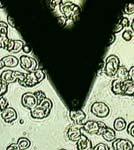
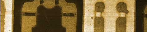
21 Sample 1 Optical images of sample 1. The failed 48 th transistor is marked with a blue circle. Agilent General Audience Page 21
, and capacitance")
 and FETs 45 48 (left).")

 indicates a")
22 Sample 1 Topography (top), dopant concentration (middle), and capacitance (bottom) images of scans across FETs (right) and FETs (left). Dopant density images (middle) clearly show a difference on the 48 th FET from all others (43 47). The missing dark area (p dopant) indicates a problem in the channel of the 48 th FET. Agilent General Audience Page 22
, and capacitance (bottom) images of scans")


23 Sample 1 Topography (top), dopant concentration (middle), and capacitance (bottom) images of scans across FETs (right) and FETs (left). Like the last slide, dopant concentration images also show a noticeable difference on the 48 th FET from all others. Capacitance image of the 48 th FET appears some difference from others as well. The result here is consistent with the observation obtained on July 10. Agilent General Audience Page 23
24 SiGe device Topography Capacitance dc/dv Page 24
25 InGaP/GaAs heterojunction bipolar transistor Topography Impedance Different regions from the emitter-side contact layer (7 and 8) to the subcollector layer (1) with different doping levels were clearly resolved in the impedance image. (Sample courtesy of T. Low) Page 25
26 Biological sample Bacteria cells of geobacter sulfurreducens Topography Impedance Sample courtesy of N. Hansmeier, T. Chau, R. Ros, and S. Lindsay at Arizona State University. Page 26
27 Summary A new technique, which integrates AFM with a professional network analyzer, has been developed. scanning microwave microscopy Mapping impedance, capacitance, dielectric constants, etc. SNMM Measuring two-dimensional dopant density of semiconductors. SCM High sensitivity with resolution ultimately limited by the probe. Metals, semiconductors, dielectric materials, ferroelectric materials, insulators, and even biological samples. Page 27


")
28 Agilent Technologies = Innovation in Measurements We are presenting a state of the art AFM/SMM microscope to enable material measurements at the Nanoscale + = Coaxial cable Coaxial Resonator Sample The MW diplexer Ground/Shield Sample scanning AFM in X and Y and Z (closed loop) Network Analyzer Page 28
Expanding Impedance Measurement to Nanoscale:
 Expanding Impedance Measurement to Nanoscale: Coupling the Power of Scanning Probe Microscopy with Performance Network Analyzer (PNA) Hassan Tanbakuchi Senior Research Scientist Agilent Technologies Agilent
Agilent Technologies Gli analizzatori di reti della serie-x
 Agilent Technologies Gli analizzatori di reti della serie-x Luigi Fratini 1 Introducing the PNA-X Performance Network Analyzer For Active Device Test 500 GHz & beyond! 325 GHz 110 GHz 67 GHz 50 GHz 43.5
Cutting-edge Atomic Force Microscopy techniques for large and multiple samples
 Cutting-edge Atomic Force Microscopy techniques for large and multiple samples Study of up to 200 mm samples using the widest set of AFM modes Industrial standards of automation A unique combination of
Keysight Technologies Scanning Microwave Microscopy Solutions for Quantitative Semiconductor Device Characterization.
 Keysight Technologies Scanning Microwave Microscopy Solutions for Quantitative Semiconductor Device Characterization Application Note Introduction The scanning microwave microscope (SMM) merges the nanoscale
Keysight Technologies Scanning Microwave Microscope Mode. Application Note
 Keysight Technologies Scanning Microwave Microscope Mode Application Note Introduction Measuring electromagnetic properties of materials can provide insight into applications in many areas of science and
An advanced impedance calibration method for nanoscale microwave imaging
 An advanced impedance calibration method for nanoscale microwave imaging M. Kasper 1, *, G. Gramse 2 and F. Kienberger 1 1 Keysight Technologies Austria GmbH, Keysight Labs, Gruberstrasse 40, 4020 Linz,
Keysight Technologies 5500 AFM Controller Upgrade. Data Sheet
 Keysight Technologies 5500 AFM Controller Upgrade Data Sheet 02 Keysight 5500 AFM Controller Upgrade - Data Sheet Upgrade Overview The Keysight 5500 AFM Controller Upgrade offers a tremendously convenient
Using Nanoelectrical Solutions to expand the capability of AFM Dr. Peter De Wolf
 Using Nanoelectrical Solutions to expand the capability of AFM Dr. Peter De Wolf peter.dewolf@bruker.com 2 Atomic Force Microscopy (AFM) Microscopy technique based on raster-scanning and small tipsample
SPM The Industry s Performance Leader High Resolution Closed-loop System Fast, Easy Tip & Sample Exchange Versatility and Value Powerful Research
 SPM The Industry s Performance Leader High Resolution Closed-loop System Fast, Easy Tip & Sample Exchange Versatility and Value Powerful Research Flexibility Atomic resolution STM image of highly-oriented
Grundlagen der Impedanzmessung
 Grundlagen der Impedanzmessung presented by Michael Benzinger Application Engineer - RF & MW Agenda Impedance Measurement Basics Impedance Basics Impedance Dependency Factors Impedance Measurement Methods
High Resolution Imaging of Nanoscale Structures by Scanning Probe Microscopy Techniques
 High Resolution Imaging of Nanoscale Structures by Scanning Probe Microscopy Techniques Prof. Marco Farina, Senior Member IEEE Dipartimento di Ingegneria dell Informazione Università Politecnica delle
Lecture 20: Optical Tools for MEMS Imaging
 MECH 466 Microelectromechanical Systems University of Victoria Dept. of Mechanical Engineering Lecture 20: Optical Tools for MEMS Imaging 1 Overview Optical Microscopes Video Microscopes Scanning Electron
Dual-channel Lock-in Amplifier Module
 Dual-channel Lock-in Amplifier Module Introduction Phase-locked amplification and demodulation techniques of weak signals have a wide range of applications in Turnable Diode Laser Absorption Spectrum (TDLAS)
Park NX-Hivac The world s most accurate and easy to use high vacuum AFM for failure analysis.
 Park NX-Hivac The world s most accurate and easy to use high vacuum AFM for failure analysis www.parkafm.com Park NX-Hivac High vacuum scanning for failure analysis applications 4 x 07 / Cm3 Current (µa)
Amateur Extra Manual Chapter 9.4 Transmission Lines
 9.4 TRANSMISSION LINES (page 9-31) WAVELENGTH IN A FEED LINE (page 9-31) VELOCITY OF PROPAGATION (page 9-32) Speed of Wave in a Transmission Line VF = Velocity Factor = Speed of Light in a Vacuum Question
Electrical Properties of Chicken Herpes Virus Based on Impedance Analysis using Atomic Force Microscopy
 Electrical Properties of Chicken Herpes Virus Based on Impedance Analysis using Atomic Force Microscopy Zhuxin Dong Ph. D. Candidate, Mechanical Engineering University of Arkansas Brock Schulte Masters
Electric polarization properties of single bacteria measured with electrostatic force microscopy
 Electric polarization properties of single bacteria measured with electrostatic force microscopy Theoretical and practical studies of Dielectric constant of single bacteria and smaller elements Daniel
Electronic Characterization of Materials Using Conductive AFM
 Electronic Characterization of Materials Using Conductive AFM Amir Moshar Electrical Measurements SKPM EFM CAFM PFM SCM Non-Contact Electrical Techniques Scanning Kelvin Probe Microscopy Electric Force
Fine structure of the inner electric field in semiconductor laser diodes studied by EFM.
 Fine structure of the inner electric field in semiconductor laser diodes studied by EFM. Phys. Low-Dim. Struct. 3/4, 9 (2001). A.Ankudinov 1, V.Marushchak 1, A.Titkov 1, V.Evtikhiev 1, E.Kotelnikov 1,
NanoFocus Inc. Next Generation Scanning Probe Technology. Tel : Fax:
 NanoFocus Inc. Next Generation Scanning Probe Technology www.nanofocus.kr Tel : 82-2-864-3955 Fax: 82-2-864-3956 Albatross SPM is Multi functional research grade system Flexure scanner and closed-loop
Prepare Sample 3.1. Place Sample in Stage. Replace Probe (optional) Align Laser 3.2. Probe Approach 3.3. Optimize Feedback 3.4. Scan Sample 3.
 Align Laser 3.2. Probe Approach 3.3. Optimize Feedback 3.4. Scan Sample 3.") CHAPTER 3 Measuring AFM Images Learning to operate an AFM well enough to get an image usually takes a few hours of instruction and practice. It takes 5 to 10 minutes to measure an image if the sample is
CHAPTER 3 Measuring AFM Images Learning to operate an AFM well enough to get an image usually takes a few hours of instruction and practice. It takes 5 to 10 minutes to measure an image if the sample is
; A=4π(2m) 1/2 /h. exp (Fowler Nordheim Eq.) 2 const
 1/2 /h. exp (Fowler Nordheim Eq.) 2 const") Scanning Tunneling Microscopy (STM) Brief background: In 1981, G. Binnig, H. Rohrer, Ch. Gerber and J. Weibel observed vacuum tunneling of electrons between a sharp tip and a platinum surface. The tunnel
Scanning Tunneling Microscopy (STM) Brief background: In 1981, G. Binnig, H. Rohrer, Ch. Gerber and J. Weibel observed vacuum tunneling of electrons between a sharp tip and a platinum surface. The tunnel
Park XE7 The most affordable research grade AFM with flexible sample handling.
 Park XE7 The most affordable research grade AFM with flexible sample handling www.parkafm.com Park Systems The Most Accurate Atomic Force Microscope Park XE7 The economical choice for innovative research
Measurement of Microscopic Three-dimensional Profiles with High Accuracy and Simple Operation
 238 Hitachi Review Vol. 65 (2016), No. 7 Featured Articles Measurement of Microscopic Three-dimensional Profiles with High Accuracy and Simple Operation AFM5500M Scanning Probe Microscope Satoshi Hasumura
Γ L = Γ S =
 TOPIC: Microwave Circuits Q.1 Determine the S parameters of two port network consisting of a series resistance R terminated at its input and output ports by the characteristic impedance Zo. Q.2 Input matching
Dr.-Ing. Ulrich L. Rohde
 Dr.-Ing. Ulrich L. Rohde Noise in Oscillators with Active Inductors Presented to the Faculty 3 : Mechanical engineering, Electrical engineering and industrial engineering, Brandenburg University of Technology
Park NX20 The leading nano metrology tool for failure analysis and large sample research.
 The Most Accurate Atomic Force Microscope Park NX20 The leading nano metrology tool for failure analysis and large sample research www.parkafm.com The Most Accurate Atomic Force Microscope Park NX20 The
- Near Field Scanning Optical Microscopy - Electrostatic Force Microscopy - Magnetic Force Microscopy
 - Near Field Scanning Optical Microscopy - Electrostatic Force Microscopy - Magnetic Force Microscopy Yongho Seo Near-field Photonics Group Leader Wonho Jhe Director School of Physics and Center for Near-field
Optical Microscope. Active anti-vibration table. Mechanical Head. Computer and Software. Acoustic/Electrical Shield Enclosure
 Optical Microscope On-axis optical view with max. X magnification Motorized zoom and focus Max Field of view: mm x mm (depends on zoom) Resolution : um Working Distance : mm Magnification : max. X Zoom
RHK Technology. Application Note: Kelvin Probe Force Microscopy with the RHK R9. ω mod allows to fully nullify any contact potential difference
 Peter Milde 1 and Steffen Porthun 2 1-Institut für Angewandte Photophysik, TU Dresden, D-01069 Dresden, Germany 2-RHK Technology, Inc. Introduction Kelvin-probe force microscopy (KPFM) is an operation
Rebirth of Force Spectroscopy: Advanced Nanomechanical, Electrical, Optical, Thermal and Piezoresponse Studies
 HybriD Mode Rebirth of Force Spectroscopy: Advanced Nanomechanical, Electrical, Optical, Thermal and Piezoresponse Studies Fast Quantitative Nanomechanical Measurements and Force Volume Simultaneous Electrostatic
Microscopic Structures
 Microscopic Structures Image Analysis Metal, 3D Image (Red-Green) The microscopic methods range from dark field / bright field microscopy through polarisation- and inverse microscopy to techniques like
PFM Experiments with High Voltage DC/AC Bias
 PFM Experiments with High Voltage DC/AC Bias Support Note Shijie Wu and John Alexander Agilent Technologies Introduction Piezoelectric force microscopy (PFM) has found major applications in the study of
Lateral Force: F L = k L * x
 Scanning Force Microscopy (SFM): Conventional SFM Application: Topography measurements Force: F N = k N * k N Ppring constant: Spring deflection: Pieo Scanner Interaction or force dampening field Contact
Chapter 6. FM Circuits
 Chapter 6 FM Circuits Topics Covered 6-1: Frequency Modulators 6-2: Frequency Demodulators Objectives You should be able to: Explain the operation of an FM modulators and demodulators. Compare and contrast;
The Most Accurate Atomic Force Microscope. Park NX20 The leading nano metrology tool for failure analysis and large sample research.
 The Most Accurate Atomic Force Microscope Park NX20 The leading nano metrology tool for failure analysis and large sample research www.parkafm.com Park Systems The Most Accurate Atomic Force Microscope
Industrial Electronics
 Job Ready Assessment Blueprint Industrial Electronics Test Code: 2051 / Version: 01 Measuring What Matters Specific Competencies and Skills Tested in this Assessment: DC Electricity Demonstrate the ability
Agilent Technologies Scanning Probe Microscope. User s Guide. Agilent Technologies
 Agilent Technologies 5500 Scanning Probe Microscope User s Guide Agilent Technologies Notices Agilent Technologies, Inc. 2008 No part of this manual may be reproduced in any form or by any means (including
INDIAN INSTITUTE OF TECHNOLOGY BOMBAY
 IIT Bombay requests quotations for a high frequency conducting-atomic Force Microscope (c-afm) instrument to be set up as a Central Facility for a wide range of experimental requirements. The instrument
Advanced Nanoscale Metrology with AFM
 Advanced Nanoscale Metrology with AFM Sang-il Park Corp. SPM: the Key to the Nano World Initiated by the invention of STM in 1982. By G. Binnig, H. Rohrer, Ch. Gerber at IBM Zürich. Expanded by the invention
Pattern Transfer CD-AFM. Resist Features on Poly. Poly Features on Oxide. Quate Group, Stanford University
 Resist Features on Poly Pattern Transfer Poly Features on Oxide CD-AFM The Critical Dimension AFM Boot -Shaped Tip Tip shape is optimized to sense topography on vertical surfaces Two-dimensional feedback
MSE 410/ECE 340: Electrical Properties of Materials Fall 2016 Micron School of Materials Science and Engineering Boise State University
 MSE 410/ECE 340: Electrical Properties of Materials Fall 2016 Micron School of Materials Science and Engineering Boise State University Practice Final Exam 1 Read the questions carefully Label all figures
Scattered thoughts on Scattering Parameters By Joseph L. Cahak Copyright 2013 Sunshine Design Engineering Services
 Scattered thoughts on Scattering Parameters By Joseph L. Cahak Copyright 2013 Sunshine Design Engineering Services Scattering parameters or S-parameters (aka Spars) are used by RF and microwave engineers
The Most Accurate Atomic Force Microscope. Park XE15 Power and versatility, brilliantly combined.
 The Most Accurate Atomic Force Microscope Park XE15 Power and versatility, brilliantly combined. www.parkafm.com Park XE15 Increase your productivity with our powerfully versatile atomic force microscope
1 FUNDAMENTAL CONCEPTS What is Noise Coupling 1
 Contents 1 FUNDAMENTAL CONCEPTS 1 1.1 What is Noise Coupling 1 1.2 Resistance 3 1.2.1 Resistivity and Resistance 3 1.2.2 Wire Resistance 4 1.2.3 Sheet Resistance 5 1.2.4 Skin Effect 6 1.2.5 Resistance
New Ultra-Fast Noise Parameter System... Opening A New Realm of Possibilities in Noise Characterization
 New Ultra-Fast Noise Parameter System... Opening A New Realm of Possibilities in Noise Characterization David Ballo Application Development Engineer Agilent Technologies Gary Simpson Chief Technology Officer
Exercise 1: RF Stage, Mixer, and IF Filter
 SSB Reception Analog Communications Exercise 1: RF Stage, Mixer, and IF Filter EXERCISE OBJECTIVE DISCUSSION On the circuit board, you will set up the SSB transmitter to transmit a 1000 khz SSB signal
1. What is the unit of electromotive force? (a) volt (b) ampere (c) watt (d) ohm. 2. The resonant frequency of a tuned (LRC) circuit is given by
 volt (b) ampere (c) watt (d) ohm. 2. The resonant frequency of a tuned (LRC) circuit is given by") Department of Examinations, Sri Lanka EXAMINATION FOR THE AMATEUR RADIO OPERATORS CERTIFICATE OF PROFICIENCY ISSUED BY THE DIRECTOR GENERAL OF TELECOMMUNICATIONS, SRI LANKA 2004 (NOVICE CLASS) Basic Electricity,
Department of Examinations, Sri Lanka EXAMINATION FOR THE AMATEUR RADIO OPERATORS CERTIFICATE OF PROFICIENCY ISSUED BY THE DIRECTOR GENERAL OF TELECOMMUNICATIONS, SRI LANKA 2004 (NOVICE CLASS) Basic Electricity,
Microwave and RF Engineering
 Microwave and RF Engineering Volume 1 An Electronic Design Automation Approach Ali A. Behagi and Stephen D. Turner BT Microwave LLC State College, PA 16803 Copyrighted Material Microwave and RF Engineering
NOISE IN MEMS PIEZORESISTIVE CANTILEVER
 NOISE IN MEMS PIEZORESISTIVE CANTILEVER Udit Narayan Bera Mechatronics, IIITDM Jabalpur, (India) ABSTRACT Though pezoresistive cantilevers are very popular for various reasons, they are prone to noise
Optically reconfigurable balanced dipole antenna
 Loughborough University Institutional Repository Optically reconfigurable balanced dipole antenna This item was submitted to Loughborough University's Institutional Repository by the/an author. Citation:
CONTENTS. 2.2 Schrodinger's Wave Equation 31. PART I Semiconductor Material Properties. 2.3 Applications of Schrodinger's Wave Equation 34
 CONTENTS Preface x Prologue Semiconductors and the Integrated Circuit xvii PART I Semiconductor Material Properties CHAPTER 1 The Crystal Structure of Solids 1 1.0 Preview 1 1.1 Semiconductor Materials
Instruction manual and data sheet ipca h
 1/15 instruction manual ipca-21-05-1000-800-h Instruction manual and data sheet ipca-21-05-1000-800-h Broad area interdigital photoconductive THz antenna with microlens array and hyperhemispherical silicon
Lab 4. Crystal Oscillator
 Lab 4. Crystal Oscillator Modeling the Piezo Electric Quartz Crystal Most oscillators employed for RF and microwave applications use a resonator to set the frequency of oscillation. It is desirable to
FCC Technician License Course
 FCC Technician License Course 2014-2018 FCC Element 2 Technician Class Question Pool Presented by: Tamiami Amateur Radio Club (TARC) WELCOME To the SECOND of 4, 3-hour classes presented by TARC to prepare
電子回路論第 7 回 Electric Circuits for Physicists #7
 電子回路論第 7 回 Electric Circuits for Physicists #7 東京大学理学部 理学系研究科物性研究所勝本信吾 Shingo Katsumoto Outline 4.5 Field Effect Transistors (FETs) Ch.5 Distributed constant circuits 5.1 Transmission lines 5.1.1 Coaxial
Christian Boit TUB Berlin University of Technology Sect. Semiconductor Devices. 1
 Semiconductor Device & Analysis Center Berlin University of Technology Christian Boit TUB Berlin University of Technology Sect. Semiconductor Devices Christian.Boit@TU-Berlin.DE 1 Semiconductor Device
Indian Institute of Technology Bombay
 Specifications for High Resolution Scanning Probe Microscope Item Essential measuring modes with complete hardware and software. All the modes should be demonstrated during installation & training Scanners
MEMS for RF, Micro Optics and Scanning Probe Nanotechnology Applications
 MEMS for RF, Micro Optics and Scanning Probe Nanotechnology Applications Part I: RF Applications Introductions and Motivations What are RF MEMS? Example Devices RFIC RFIC consists of Active components
THE DESIGN OF MICROWAVE OSCILLATOR BY THE METHOD OF NEGATIVE RESISTANCE
 THE DESIGN OF MICROWAVE OSCILLATOR BY THE METHOD OF NEGATIVE RESISTANCE ABSTRACT Saranya E Electronics and Telecommunication Engineering, Bharath University, (India) An electronic oscillator is an electronic
A New Noise Parameter Measurement Method Results in More than 100x Speed Improvement and Enhanced Measurement Accuracy
 MAURY MICROWAVE CORPORATION March 2013 A New Noise Parameter Measurement Method Results in More than 100x Speed Improvement and Enhanced Measurement Accuracy Gary Simpson 1, David Ballo 2, Joel Dunsmore
This paper is meant assist in the operation and understanding of the VIA Bravo Family of products.
 Abstract: This paper is meant assist in the operation and understanding of the VIA Bravo Family of products. Understanding the Display and its Readings: The VIA Bravo display provides graphical and numerical
Alejandro Mendez, Ph.D. President & CEO Mendezized Metals Corporation
 ATOMIC FORCE MICROSCOPY (AFM) PHOTO CONDUCTIVE ANALYSIS AND CALCULATION FOR REGULAR AND MENDEZIZED COMMERCIAL 24 KARATS GOLD BARS CONDUCTED IN FIVE DIFFERENT TRIPLICATE SERIES. Date: June 23, 2016 Conducted
THE JFET. Script. Discuss the JFET and how it differs from the BJT. Describe the basic structure of n-channel and p -channel JFETs
 Course: B.Sc. Applied Physical Science (Computer Science) Year & Sem.: Ist Year, Sem - IInd Subject: Electronics Paper No.: V Paper Title: Analog Circuits Lecture No.: 12 Lecture Title: Analog Circuits
Park NX-Hivac: Phase-lock Loop for Frequency Modulation Non-Contact AFM
 Park Atomic Force Microscopy Application note #21 www.parkafm.com Hosung Seo, Dan Goo and Gordon Jung, Park Systems Corporation Romain Stomp and James Wei Zurich Instruments Park NX-Hivac: Phase-lock Loop
Raman Spectroscopy and Transmission Electron Microscopy of Si x Ge 1-x -Ge-Si Core-Double-Shell Nanowires
 Raman Spectroscopy and Transmission Electron Microscopy of Si x Ge 1-x -Ge-Si Core-Double-Shell Nanowires Paola Perez Mentor: Feng Wen PI: Emanuel Tutuc Background One-dimensional semiconducting nanowires
Distinguishing Between Mechanical and Electrostatic. Interaction in Single-Pass Multifrequency Electrostatic Force
 SUPPORTING INFORMATION Distinguishing Between Mechanical and Electrostatic Interaction in Single-Pass Multifrequency Electrostatic Force Microscopy on a Molecular Material Marta Riba-Moliner, Narcis Avarvari,
Vector Network Analyzer
 Vector Network Analyzer VNA Basics VNA Roadshow Budapest 17/05/2016 Content Why Users Need VNAs VNA Terminology System Architecture Key Components Basic Measurements Calibration Methods Accuracy and Uncertainty
RECENTLY, using near-field scanning optical
 1 2 1 2 Theoretical and Experimental Study of Near-Field Beam Properties of High Power Laser Diodes W. D. Herzog, G. Ulu, B. B. Goldberg, and G. H. Vander Rhodes, M. S. Ünlü L. Brovelli, C. Harder Abstract
Lecture - 18 Transistors
 Electronic Materials, Devices and Fabrication Dr. S. Prarasuraman Department of Metallurgical and Materials Engineering Indian Institute of Technology, Madras Lecture - 18 Transistors Last couple of classes
Standard Operating Procedure
 Standard Operating Procedure Nanosurf Atomic Force Microscopy Operation Facility NCCRD Nanotechnology Center for Collaborative Research and Development Department of Chemistry and Engineering Physics The
Outline: Introduction: What is SPM, history STM AFM Image treatment Advanced SPM techniques Applications in semiconductor research and industry
 1 Outline: Introduction: What is SPM, history STM AFM Image treatment Advanced SPM techniques Applications in semiconductor research and industry 2 Back to our solutions: The main problem: How to get nm
Lab 4. Crystal Oscillator
 Lab 4. Crystal Oscillator Modeling the Piezo Electric Quartz Crystal Most oscillators employed for RF and microwave applications use a resonator to set the frequency of oscillation. It is desirable to
Application Note 5525
 Using the Wafer Scale Packaged Detector in 2 to 6 GHz Applications Application Note 5525 Introduction The is a broadband directional coupler with integrated temperature compensated detector designed for
Supplementary Figure 1 Schematic illustration of fabrication procedure of MoS2/h- BN/graphene heterostructures. a, c d Supplementary Figure 2
 Supplementary Figure 1 Schematic illustration of fabrication procedure of MoS 2 /hon a 300- BN/graphene heterostructures. a, CVD-grown b, Graphene was patterned into graphene strips by oxygen monolayer
LOW TEMPERATURE STM/AFM
 * CreaTec STM of Au(111) using a CO-terminated tip, 20mV bias, 0.6nA* LOW TEMPERATURE STM/AFM High end atomic imaging, spectroscopy and manipulation Designed and manufactured in Germany by CreaTec Fischer
Keysight Technologies 9500 AFM. Data Sheet
 Keysight Technologies 9500 AFM Data Sheet System Overview The Keysight Technologies, Inc. 9500 AFM seamlessly integrates revolutionary new software, a new high-bandwidth digital controller, and a state-of-the-art
RF Hybrid Linear Amplifier Using Diamond Heat Sink
 RF Hybrid Linear Amplifier Using Diamond Heat Sink Item Type text; Proceedings Authors Karabudak, Nafiz Publisher International Foundation for Telemetering Journal International Telemetering Conference
Investigate in magnetic micro and nano structures by Magnetic Force Microscopy (MFM)
") Investigate in magnetic micro and nano 5.3.85- Related Topics Magnetic Forces, Magnetic Force Microscopy (MFM), phase contrast imaging, vibration amplitude, resonance shift, force Principle Caution! -
Investigate in magnetic micro and nano 5.3.85- Related Topics Magnetic Forces, Magnetic Force Microscopy (MFM), phase contrast imaging, vibration amplitude, resonance shift, force Principle Caution! -
IMAGING P-N JUNCTIONS BY SCANNING NEAR-FIELD OPTICAL, ATOMIC FORCE AND ELECTRICAL CONTRAST MICROSCOPY. G. Tallarida Laboratorio MDM-INFM
 Laboratorio MDM - INFM Via C.Olivetti 2, I-20041 Agrate Brianza (MI) M D M Materiali e Dispositivi per la Microelettronica IMAGING P-N JUNCTIONS BY SCANNING NEAR-FIELD OPTICAL, ATOMIC FORCE AND ELECTRICAL
Mapping piezoelectric response in nanomaterials using a dedicated non-destructive scanning probe technique. Supporting Information
 Electronic Supplementary Material (ESI) for Nanoscale. This journal is The Royal Society of Chemistry 2017 Mapping piezoelectric response in nanomaterials using a dedicated non-destructive scanning probe
High resolution measurements The differential approach
 Electrical characterisation of nanoscale samples & biochemical interfaces: methods and electronic instrumentation High resolution measurements The differential approach Giorgio Ferrari Dipartimento di
I E I C since I B is very small
 Figure 2: Symbols and nomenclature of a (a) npn and (b) pnp transistor. The BJT consists of three regions, emitter, base, and collector. The emitter and collector are usually of one type of doping, while
Suivie de résonance: méthodes à fréquences multiples. Romain Stomp Application Scientist, Zurich Instruments AG. ZI Applications
 Suivie de résonance: méthodes à fréquences multiples Romain Stomp Application Scientist, Zurich Instruments AG Slide 1 Sommaire 1. Un peu de traitement du signal pour le SPM Détection synchrone pour le
Akiyama-Probe (A-Probe) guide
 guide") Akiyama-Probe (A-Probe) guide This guide presents: what is Akiyama-Probe, how it works, and what you can do Dynamic mode AFM Version: 2.0 Introduction NANOSENSORS Akiyama-Probe (A-Probe) is a self-sensing
Akiyama-Probe (A-Probe) guide This guide presents: what is Akiyama-Probe, how it works, and what you can do Dynamic mode AFM Version: 2.0 Introduction NANOSENSORS Akiyama-Probe (A-Probe) is a self-sensing
Agilent Technologies Impedance Measurement Handbook December 2003
 Agilent Technologies Impedance Measurement Handbook December 2003 This page intentionally left blank. The Impedance Measurement Handbook A Guide to Measurement Technology and Techniques Copyright 2000-2003
Wafer-Level Calibration & Verification up to 750 GHz. Choon Beng Sia, Ph.D. Mobile:
 Wafer-Level Calibration & Verification up to 750 GHz Choon Beng Sia, Ph.D. Email: Choonbeng.sia@cmicro.com Mobile: +65 8186 7090 2016 Outline LRRM vs SOLT Calibration Verification Over-temperature RF calibration
Micro-manipulated Cryogenic & Vacuum Probe Systems
 Janis micro-manipulated probe stations are designed for non-destructive electrical testing using DC, RF, and fiber-optic probes. They are useful in a variety of fields including semiconductors, MEMS, superconductivity,
Design and construction of an experimental setup to study ferromagnetic resonance
 Design and construction of an experimental setup to study ferromagnetic resonance Author: Borja Celma Serrano Advisor: Joan Manel Hernández Facultat de Física, Universitat de Barcelona, Diagonal 645, 08028
Understanding VCO Concepts
 Understanding VCO Concepts OSCILLATOR FUNDAMENTALS An oscillator circuit can be modeled as shown in Figure 1 as the combination of an amplifier with gain A (jω) and a feedback network β (jω), having frequency-dependent
Supplementary Materials for
 advances.sciencemag.org/cgi/content/full/2/7/e1629/dc1 Supplementary Materials for Subatomic deformation driven by vertical piezoelectricity from CdS ultrathin films Xuewen Wang, Xuexia He, Hongfei Zhu,
RFIC Design ELEN 376 Session 1
 RFIC Design ELEN 376 Session 1 Instructor: Dr. Allen Sweet April 3, 2002 Copy right 2002, elen376 1 General Information Instructor: Dr. Allen Sweet Email: allensweet@aol.com Home work/project submissions:
RFIC Design ELEN 351 Lecture 1: General Discussion
 RFIC Design ELEN 351 Lecture 1: General Discussion Instructor: Dr. Allen Sweet Copy right 2003, ELEN351 1 General Information Instructor: Dr. Allen Sweet Email: allensweet@aol.com Home work/project submissions:
Broadband Microwave Interferometry for Nondestructive Evaluation
 13th International Symposium on Nondestructive Characterization of Materials (NDCM-XIII), 20-24 May 2013, Le Mans, France www.ndt.net/?id=15526 Broadband Microwave Interferometry for Nondestructive Evaluation
Nanosurf easyscan 2 FlexAFM
 Nanosurf easyscan 2 FlexAFM Your Versatile AFM System for Materials and Life Science www.nanosurf.com The new Nanosurf easyscan 2 FlexAFM scan head makes measurements in liquid as simple as measuring in
Near-field Optical Microscopy
 Near-field Optical Microscopy R. Fernandez, X. Wang, N. Li, K. Parker, and A. La Rosa Physics Department Portland State University Portland, Oregon Near-Field SPIE Optics Microscopy East 2005 Group PSU
Millimeter- and Submillimeter-Wave Planar Varactor Sideband Generators
 Millimeter- and Submillimeter-Wave Planar Varactor Sideband Generators Haiyong Xu, Gerhard S. Schoenthal, Robert M. Weikle, Jeffrey L. Hesler, and Thomas W. Crowe Department of Electrical and Computer
MICROWAVE ENGINEERING-II. Unit- I MICROWAVE MEASUREMENTS
 MICROWAVE ENGINEERING-II Unit- I MICROWAVE MEASUREMENTS 1. Explain microwave power measurement. 2. Why we can not use ordinary diode and transistor in microwave detection and microwave amplification? 3.
Evaluation of Package Properties for RF BJTs
 Application Note Evaluation of Package Properties for RF BJTs Overview EDA simulation software streamlines the development of digital and analog circuits from definition of concept and estimation of required
Solid State Device Fundamentals
 Solid State Device Fundamentals 4.4. Field Effect Transistor (MOSFET) ENS 463 Lecture Course by Alexander M. Zaitsev alexander.zaitsev@csi.cuny.edu Tel: 718 982 2812 4N101b 1 Field-effect transistor (FET)