Fine structure of the inner electric field in semiconductor laser diodes studied by EFM.
|
|
|
- Madeleine Chase
- 5 years ago
- Views:
Transcription
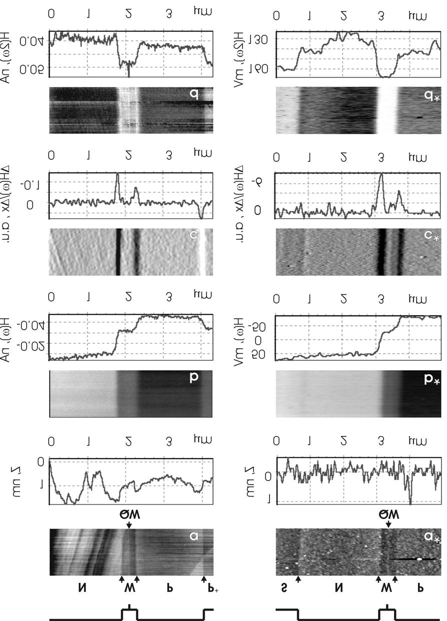
1 Fine structure of the inner electric field in semiconductor laser diodes studied by EFM. Phys. Low-Dim. Struct. 3/4, 9 (2001). A.Ankudinov 1, V.Marushchak 1, A.Titkov 1, V.Evtikhiev 1, E.Kotelnikov 1, A.Egorov 1, H.Riechert 2, H.Huhtinen 3, R.Laiho 3 1 Ioffe PTI, Polytechnicheskaya 26, St.-Petersburg, , Russia 2 Infineon Technologies AG, Corporate Research, D München, Germany 3 Wihuri Physical Laboratory, Turku University, Turku, FIN20014, Finland Alexander.Ankudinov@pop.ioffe.rssi.ru; FAX Abstract. Electrostatic force microscopy in dynamical contact and noncontact modes is employed to study the distribution of the electric field and capacitance at the cleavages of AlGaAs/GaAs based p- i-n laser diode heterostructures. The fine structure of the inner electric field located at the i- waveguide of the laser heteroctructure is revealed and investigated under forward and backward biases applied to the diode. The redistribution of the electric field in favor of i-waveguide/p-emitter interface is observed at high level of injected current. When the injected current increase, the growth of the capacitance signal at the i-waveguide is also detected, that may reflect the injected carriers distribution. The inner electric characteristics of the semiconductor devices under the conditions close to the operation are the subject of intensive theoretical and experimental interest. Very attractive possibilities on the high resolution mapping of the electric field and capacitance distribution in the semiconductor structures are provided by the relatively new method of electrostatic force microscopy (EFM)[1]. In the first studies [2,3,4] focused on the application of EFM to probe electric characteristics of semiconductor light emitting devices, the main attention was concentrated on the potential profiles across the devices, the capacitance distributions had a minor attention. Besides, the authors used noncontact mode electrostatic force microscopy (NC EFM), when the probe performs resonant oscillations at some distance from the surface. Recently the dynamic contact mode electrostatic force microscopy (DC EFM) was developed [5], in which the probe is in the constant contact with the studied surface. In this case the distance between the probe and the surface is minimized, what may provide better sensitivity and resolution of the EFM. Successful attempt to apply
2 the DC EFM for studying the semiconductors laser diodes is presented in our recent work [6]. In this work we have performed EFM studies in DC and NC modes to investigate the electric field and capacitance distributions on the cross-sections of the AlGaAs/GaAs based p-i-n laser diodes under the applied forward and backward biases. We show that on the atomically flat cleavages of laser heterostructures both modes demonstrate self consisting results. The electric field distribution in the studied laser structures has two field maximums localized at the n-emitter/i-waveguide and p-emitter/i-waveguide interfaces. At the low level of the injection current the inner electric field induced by the applied bias is concentrated mainly in the vicinity of the n-emitter/i-waveguide interface, while at the high level of injection it is redistributed in favor of the p-emitter/i-waveguide interface. With increasing forward bias the growth and broadening of the capacitance signal at the undoped waveguide region is also observed, that may reflect the injected carriers distribution. Consider the main principles of the EFM [2-5]. If the conductive probe is at some potential U relative to the sample, then the acting electrostatic force can be written as: F el =1/2 d(c ps U 2 )/dz (1), where C ps is the capacitance between the probe and sample and an axe z is perpendicular to the sample surface. The potential U between the probe and sample surface may be written as U= U dc +U ac cos(ωt)+v ps, where U dc is external dc bias, U ac cos(ωt) is ac bias and V ps is the contact potential between the probe and the sample. Substitution of this expression into formula (1) shows, that the resulting force F el will have three components: one static and two alternating, oscillating at the frequencies ω and 2ω. The oscillating components are given by: F(ω)= (dc ps /dz)(u dc +V ps )U ac cos(ωt) (2), F(2ω)=1/4(dC ps /dz)u 2 ac cos(2ωt) (3). In the EFM method the oscillating components of the electrostatic force induce mechanical oscillations of the AFM probe. The first and the second harmonics (H(ω), H(2ω)) of oscillations, which are the two main EFM signals, can be detected by lock-in technique. H(ω) depends mainly on the probe-surface potential difference, H(2ω) is proportional to the corresponding capacitance. In addition to the EFM signals the AFM topography data can be measured. It is worth to note that in NC mode of EFM the oscillations of the probe are almost free, but in DC mode the cantilever is fixed at both ends. In the last case the amplitude of H(ω) and H(2ω) signals is determined not only by the corresponding components of the force F(ω) and F(2ω), but also by the mechanical hardness
3 k eff of the probe-surface contact [5]. Due to dependence of k eff on the surface curvature, the DC EFM signals may be mixed with the topographic effect. A straightforward way to suppress this mixing is to study atomically flat surfaces, what requires a careful preparation of the laser heterostructure cleavage. We have performed measurements in DC mode on the P4-SPM (NT-MDT) microscope and in NC mode on the AFM system Autoprobe CP Research (ThermoMicroscopes). The ac bias is applied to the probe tip made from heavily doped Si at a typical frequency of around 50KHz (300KHz) and a voltage amplitude of 1V (3V), correspondingly in NC (DC) modes of EFM. The NC EFM signals are analyzed through a Stanford Lock-in Amplifier 8230, the lock-in amplifier built in the resonant module of P4- SPM is used for the DC EFM signals detection. The studied lasers are biased by the constant voltage source built in the microscopes. Figure 1 shows typical sets of the AFM/EFM data used in our work obtained on the cleaved surfaces of two p-i-n laser diodes. The left set of data characterizes the first laser and was measured in DC mode ( images a-d); the second laser (the right set of data) was probed in NC mode (images a*-d*). The structures are similar and consist of an n-doped GaAs substrate (S), an n-doped (Si) 2µm-thick AlGaAs emitter (N), an undoped 0.4 µm-thick GaAs i-waveguide (W) centered with 9nm strained quantum well (QW), a p-doped (Be) 2µm-thick AlGaAs emitter (P) followed by heavily doped p-gaas contact layer (P + ). The topography data images of both structures reveal all the main layers the lasers consist of. The darker contrast corresponds to the depression of the surface relief. The waveguide regions of the structures are several angstroms lower then n- and p- emitters due to known difference in oxide layer thickness on GaAs and AlGaAs [7]. The bright line in the middle of the waveguide corresponds to the compressed InGaNAs (left image) and InGaAs (right image) QWs. As it was shown earlier, thin compressed layers can noticeably extrude out on the cleavage [8]. The DC mode topography image (Figure 1a) has better spatial resolution, than the NC mode topography image (Figure 1a*). From the profile below the Figure 1a one can evaluate approximately 1 angstrom elevation of the QW over the cleavage. Some smearing of the atomic scale variations in the cleavage relief in NC mode topography data seems to be due to the influence of the contamination layer covering the surface in air. In DC mode the probe tip can penetrate through this soft layer, and it does not prevent to map the fine features of the relief. In Figure 1 b-d (DC mode) and b*-d* (NC mode) the variations of the EFM signals over the studied surface areas are presented. The data were measured at the negative dc bias applied to the n-contact of the lasers, when n-p junctions were almost open. The H(ω) signal
4 (potential) images and corresponding profiles in Figures 1b,b* taken in different modes of EFM are almost identical to each other. In both cases the signal has the shape of the double step, with the central plateau corresponding well to the waveguide regions. The visual changes of the H(ω) signal take place at the interfaces of the waveguides with the n- and p- emitter layers, what means that the main drop of the applied voltage occurs there. It is convenient also to analyze the H(ω)/ x data that are calculated numerically along the direction x perpendicular to the interfaces. The meaning of the H(ω)/ x data is the electric field magnitude at the surface in the direction perpendicular to the interfaces. Figures 1c,c* show the images and profiles of H(ω)/ x. The distributions of the electric field have two spikes whose extremums are localized near the waveguide interfaces, while at the waveguide centers the electric field is significantly decreased. The contributions of the spikes at the n- emitter/i-waveguide and i-waveguide/p-emitter interfaces into the inner electric field redistribution under the applied voltage will be considered below. Good correspondence between the measurements in DC and NC modes is also seen in the variations of the H(2ω) signal (capacitance). The H(2ω) signal images and profiles are shown in Figure 1d,d*. The white bands in the right (left) part of the image in Figure 1d (1d*) is attributed to the p+- GaAs contact layer (n-gaas substrate), see also the corresponding topography images in Figure 1a (1a*). An increase of the capacitance at the GaAs compared to the AlGaAs emitters is related to the thinner native oxide on GaAs [7]. The capacitance at the substrate, the emitter layers and p+ contact layer does not depend on the applied bias. However, the applied bias affects strongly the capacitance at the waveguide region, see the wide ~0.4 µm plateau in capacitance signal that coincides with the position of the waveguide. For the laser structure studied by DC EFM (Figure 1d), the additional peak in the H(2ω) signal is observed at the position of the QW. It may be caused by the contribution of the topographic effect in the capacitance signal [5]. In the topography image (Figure 1a) the QW is revealed as small elevation of the relief. Similar coupling between topography and capacitance is responsible for an enhanced contrast of the waveguide interfaces in H(2ω) image (Figure 1d), since in the topography image (Figure 1a) the waveguide interfaces correspond to the borders of the depression in the relief. The comparison of the DC and NC modes of EFM can be summarized as follows. In this study only inessential differences in facilities of both EFM modes have been found. Under the atmospheric conditions, the atomic scale variations of the surface relief can be better resolved in DC mode, that is less sensitive to the surface contamination layer. From
5 the other side, similar signal to noise ratio of the EFM signals is obtained at lower ac amplitudes of excitation (0.5-1 V) in NC mode, than in DC mode (~3 V). To analyze the inner electric field and the capacitance distribution in the AlGaAs/GaAs based laser, we present in Figure 2 the profiles of H(ω)/ x and H(2ω) signals taken under different applied bias. It was already mentioned that the H(ω)/ x data (Figure 2a) are related with the electric field at the surface in the direction perpendicular to the interfaces. Variations of this field should reflect variations of the inner electrical field in laser diodes in the same direction. Without bias (a profile taken at 0.05V) the distribution of the electric field is symmetric and formed by two spikes whose extremums are localized near the waveguide interfaces. For the low level of injection current, the inner electric field is concentrated at the n-emitter/i-waveguide interface (the left spike in the profiles taken at 0.25V, -0.35V and 0.75V is mainly changed). However, under the high level of injection, the redistribution of the inner electric field in favor of the i-waveguide/p-emitter interface is observed (the right spike in the profile taken at 1.05V is deeper than the left one). The profiles of the H(2ω) signal (capacitance) are shown in Figure 2b. The applied bias affects strongly the capacitance at the waveguide region. For the backward biases, the signal has low magnitude. Under the forward bias of approximately 0.35V, there appears at the middle of the waveguide the spike in the H(2ω) signal, which amplitude is higher than the signal level at the surrounding emitters. The spike grows in height and broadens with increasing forward bias, and at 1.05V it s top has a shape of a wide ~0.4 µm plateau that coincides well with the position of the waveguide. It is interesting to stress the graduate increase in the level of the H(2ω) signal at the waveguide region with the transition from the low level to the high level of injection. We believe that this effect is related to the carriers injection into the waveguide and can be used to study the injected carriers distribution. In conclusion, using EFM method we have revealed the fine structures of the inner electric field in AlGaAs/GaAs based p-i-n lasers. It consists of the two spikes at the waveguide/emitters interface, whose relative contribution can be different for forward and backward biases. We have found a strong increase in the capacitance of the waveguide surface area in forward biased laser, that can be related to the level of the injected current. We have also performed a comparison of the DC and NC modes of EFM, and showed that at the atomically flat surface of the laser heterostructures both modes give trusted information. The work was supported by the Program of the Ministry of Science of RF Physics of Solid State Nanostructures and by RFBR (grant N ).
6 Figure captions Figure 1. The EFM studies in DC and NC (*) modes of two similar laser heterostructures. The images and profiles a,a* are the topography data; b,b* - the H(ω) signal (surface potential); c,c* - the variations of the H(ω)/ x magnitude (electric field); d,d* - the H(2ω) signal (capacitance). The n-p junctions of both lasers are forward biased. The simplified energy band schematics of the lasers are given at the top of the corresponding set of the EFM data. Figure 2. The dependence of the inner electric field and the capacitance distribution on the applied bias. The H(ω)/ x (a) and the H(2ω) (b) set of profiles taken at different biases. The dc voltage is applied to the n-contact of the laser structure. The simplified energy band schematics of the laser are given at the top of the corresponding set of the profiles.
7
8
9 References [1] M.Nonemacher, M.P.O Boyle, H.K.Wickramasinghe, Appl.Phys.Lett. 58 (1991), 2091 [2] R.Shikler, T.Meoded, N.Fried, Y.Rosenwaks, Appl.Phys.Lett. 74 (1999), 2972 [3] G.Leveque, P.Girard, E.Skouri, D.Yarekha, Appl.Surf.Sci. 157 (2000), 251 [4] F.Robin, H.Jacobs, O.Homan, A.Stemmer, W.Bächtold, Appl.Phys.Lett. 76 (2000), 2907 [5] J.W.Hong, Sang-il Park, Z.G.Khim, Rev.Sci.Instr. 70 (1999), 1735 [6] A.V.Ankudinov, E.Y.Kotelnikov, A.A.Kanzelson, V.P.Evtikhiev, A.N.Titkov, Semiconductors 35, in press (2001) [7] A.V.Ankudinov, V.P.Evtikhiev, V.E.Tokranov, V.P.Ulin, A.N.Titkov, Semiconductors 33 (1999), 555 [8] A.V.Ankudinov, A.N.Titkov, T.V.Shubina, S.V.Ivanov, P.S.Kop ev, H.-J.Lugauer, G.Reuscher, M.Keim, A.Waag, G.Landwehr, Appl.Phys.Lett. 75 (1999), 2626
IMAGING P-N JUNCTIONS BY SCANNING NEAR-FIELD OPTICAL, ATOMIC FORCE AND ELECTRICAL CONTRAST MICROSCOPY. G. Tallarida Laboratorio MDM-INFM
 Laboratorio MDM - INFM Via C.Olivetti 2, I-20041 Agrate Brianza (MI) M D M Materiali e Dispositivi per la Microelettronica IMAGING P-N JUNCTIONS BY SCANNING NEAR-FIELD OPTICAL, ATOMIC FORCE AND ELECTRICAL
- Near Field Scanning Optical Microscopy - Electrostatic Force Microscopy - Magnetic Force Microscopy
 - Near Field Scanning Optical Microscopy - Electrostatic Force Microscopy - Magnetic Force Microscopy Yongho Seo Near-field Photonics Group Leader Wonho Jhe Director School of Physics and Center for Near-field
RECENTLY, using near-field scanning optical
 1 2 1 2 Theoretical and Experimental Study of Near-Field Beam Properties of High Power Laser Diodes W. D. Herzog, G. Ulu, B. B. Goldberg, and G. H. Vander Rhodes, M. S. Ünlü L. Brovelli, C. Harder Abstract
Characterizing the Sensitivity of a Hall Sensor
 Hall Sensor Homer L. Dodge Department of Physics and Astronomy University of Oklahoma July 30 th, 2018 s Field What are s? s are devices that utilize the to measure magnetic fields Made from semiconductors
SUPPLEMENTARY INFORMATION
 SUPPLEMENTARY INFORMATION Supplementary Information Real-space imaging of transient carrier dynamics by nanoscale pump-probe microscopy Yasuhiko Terada, Shoji Yoshida, Osamu Takeuchi, and Hidemi Shigekawa*
Lecture 20: Optical Tools for MEMS Imaging
 MECH 466 Microelectromechanical Systems University of Victoria Dept. of Mechanical Engineering Lecture 20: Optical Tools for MEMS Imaging 1 Overview Optical Microscopes Video Microscopes Scanning Electron
Physics of Waveguide Photodetectors with Integrated Amplification
 Physics of Waveguide Photodetectors with Integrated Amplification J. Piprek, D. Lasaosa, D. Pasquariello, and J. E. Bowers Electrical and Computer Engineering Department University of California, Santa
Scanning Microwave. Expanding Impedance Measurements to the Nanoscale: Coupling the Power of Scanning Probe Microscopy with the PNA
 Agilent Technologies Scanning Microwave Microscopy (SMM) Expanding Impedance Measurements to the Nanoscale: Coupling the Power of Scanning Probe Microscopy with the PNA Presented by: Craig Wall PhD Product
15 Transit Time and Tunnel NDR Devices
 15 Transit Time and Tunnel NDR Devices Schematics of Transit-time NDR diode. A packet of carriers (e.g., electrons) is generated in a confined and narrow zone (generation region) and injected into the
attosnom I: Topography and Force Images NANOSCOPY APPLICATION NOTE M06 RELATED PRODUCTS G
 APPLICATION NOTE M06 attosnom I: Topography and Force Images Scanning near-field optical microscopy is the outstanding technique to simultaneously measure the topography and the optical contrast of a sample.
SUPPLEMENTARY INFORMATION
 Figure S. Experimental set-up www.nature.com/nature Figure S2. Dependence of ESR frequencies (GHz) on a magnetic field (G) applied in different directions with respect to NV axis ( θ 2π). The angle with
Luminous Equivalent of Radiation
 Intensity vs λ Luminous Equivalent of Radiation When the spectral power (p(λ) for GaP-ZnO diode has a peak at 0.69µm) is combined with the eye-sensitivity curve a peak response at 0.65µm is obtained with
Optodevice Data Book ODE I. Rev.9 Mar Opnext Japan, Inc.
 Optodevice Data Book ODE-408-001I Rev.9 Mar. 2003 Opnext Japan, Inc. Section 1 Operating Principles 1.1 Operating Principles of Laser Diodes (LDs) and Infrared Emitting Diodes (IREDs) 1.1.1 Emitting Principles
NANOSCOPIC EVALUATION OF MICRO-SYSTEMS
 NANOSCOPIC EVALUATION OF MICRO-SYSTEMS A. Altes 1, L.J. Balk 1, H.L. Hartnagel 2, R. Heiderhoff 1, K. Mutamba 2, and Ch. Thomas 1 1 Bergische Universität Wuppertal, Lehrstuhl für Elektronik, Wuppertal,
MSE 410/ECE 340: Electrical Properties of Materials Fall 2016 Micron School of Materials Science and Engineering Boise State University
 MSE 410/ECE 340: Electrical Properties of Materials Fall 2016 Micron School of Materials Science and Engineering Boise State University Practice Final Exam 1 Read the questions carefully Label all figures
RHK Technology. Application Note: Kelvin Probe Force Microscopy with the RHK R9. ω mod allows to fully nullify any contact potential difference
 Peter Milde 1 and Steffen Porthun 2 1-Institut für Angewandte Photophysik, TU Dresden, D-01069 Dresden, Germany 2-RHK Technology, Inc. Introduction Kelvin-probe force microscopy (KPFM) is an operation
Prepared by: Dr. Rishi Prakash, Dept of Electronics and Communication Engineering Page 1 of 5
 Microwave tunnel diode Some anomalous phenomena were observed in diode which do not follows the classical diode equation. This anomalous phenomena was explained by quantum tunnelling theory. The tunnelling
Integrated High Speed VCSELs for Bi-Directional Optical Interconnects
 Integrated High Speed VCSELs for Bi-Directional Optical Interconnects Volodymyr Lysak, Ki Soo Chang, Y ong Tak Lee (GIST, 1, Oryong-dong, Buk-gu, Gwangju 500-712, Korea, T el: +82-62-970-3129, Fax: +82-62-970-3128,
Lecture 18: Photodetectors
 Lecture 18: Photodetectors Contents 1 Introduction 1 2 Photodetector principle 2 3 Photoconductor 4 4 Photodiodes 6 4.1 Heterojunction photodiode.................... 8 4.2 Metal-semiconductor photodiode................
Electric polarization properties of single bacteria measured with electrostatic force microscopy
 Electric polarization properties of single bacteria measured with electrostatic force microscopy Theoretical and practical studies of Dielectric constant of single bacteria and smaller elements Daniel
Examination Optoelectronic Communication Technology. April 11, Name: Student ID number: OCT1 1: OCT 2: OCT 3: OCT 4: Total: Grade:
 Examination Optoelectronic Communication Technology April, 26 Name: Student ID number: OCT : OCT 2: OCT 3: OCT 4: Total: Grade: Declaration of Consent I hereby agree to have my exam results published on
UNIT-III Bipolar Junction Transistor
 DC UNT-3.xplain the construction and working of JT. UNT- ipolar Junction Transistor A bipolar (junction) transistor (JT) is a three-terminal electronic device constructed of doped semiconductor material
Constant Frequency / Lock-In (AM-AFM) Constant Excitation (FM-AFM) Constant Amplitude (FM-AFM)
 Constant Excitation (FM-AFM) Constant Amplitude (FM-AFM)") HF2PLL Phase-locked Loop Connecting an HF2PLL to a Bruker Icon AFM / Nanoscope V Controller Zurich Instruments Technical Note Keywords: AM-AFM, FM-AFM, AFM control Release date: February 2012 Introduction
HF2PLL Phase-locked Loop Connecting an HF2PLL to a Bruker Icon AFM / Nanoscope V Controller Zurich Instruments Technical Note Keywords: AM-AFM, FM-AFM, AFM control Release date: February 2012 Introduction
ECE 340 Lecture 29 : LEDs and Lasers Class Outline:
 ECE 340 Lecture 29 : LEDs and Lasers Class Outline: Light Emitting Diodes Lasers Semiconductor Lasers Things you should know when you leave Key Questions What is an LED and how does it work? How does a
Key Questions. What is an LED and how does it work? How does a laser work? How does a semiconductor laser work? ECE 340 Lecture 29 : LEDs and Lasers
 Things you should know when you leave Key Questions ECE 340 Lecture 29 : LEDs and Class Outline: What is an LED and how does it How does a laser How does a semiconductor laser How do light emitting diodes
Field Effect Transistors (npn)
") Field Effect Transistors (npn) gate drain source FET 3 terminal device channel e - current from source to drain controlled by the electric field generated by the gate base collector emitter BJT 3 terminal
Field Effect Transistors (npn) gate drain source FET 3 terminal device channel e - current from source to drain controlled by the electric field generated by the gate base collector emitter BJT 3 terminal
Department of Electrical Engineering IIT Madras
 Department of Electrical Engineering IIT Madras Sample Questions on Semiconductor Devices EE3 applicants who are interested to pursue their research in microelectronics devices area (fabrication and/or
Review of Semiconductor Physics
 Review of Semiconductor Physics k B 1.38 u 10 23 JK -1 a) Energy level diagrams showing the excitation of an electron from the valence band to the conduction band. The resultant free electron can freely
Supplementary Materials for
 advances.sciencemag.org/cgi/content/full/4/2/e1700324/dc1 Supplementary Materials for Photocarrier generation from interlayer charge-transfer transitions in WS2-graphene heterostructures Long Yuan, Ting-Fung
Electronic Characterization of Materials Using Conductive AFM
 Electronic Characterization of Materials Using Conductive AFM Amir Moshar Electrical Measurements SKPM EFM CAFM PFM SCM Non-Contact Electrical Techniques Scanning Kelvin Probe Microscopy Electric Force
S1. Current-induced switching in the magnetic tunnel junction.
 S1. Current-induced switching in the magnetic tunnel junction. Current-induced switching was observed at room temperature at various external fields. The sample is prepared on the same chip as that used
Chapter 6. Silicon-Germanium Technologies
 Chapter 6 licon-germanium Technologies 6.0 Introduction The design of bipolar transistors requires trade-offs between a number of parameters. To achieve a fast base transit time, hence achieving a high
EJERCICIOS DE COMPONENTES ELECTRÓNICOS. 1 er cuatrimestre
 EJECICIOS DE COMPONENTES ELECTÓNICOS. 1 er cuatrimestre 2 o Ingeniería Electrónica Industrial Juan Antonio Jiménez Tejada Índice 1. Basic concepts of Electronics 1 2. Passive components 1 3. Semiconductors.
SEM CHARACTERIZATION OF MULTILAYER STRUCTURES
 Vol. 83 (1993) ACTA PHYSICA POLONICA A No 1 SEM CHARACTERIZATION OF MULTILAYER STRUCTURES V.V. ARISTOV, N.N. DRYOMOVA, V.A. KIREEV, I.I. RAZGONOV AND E.B. YAKIMOV Institute of Microelectronics Technology
2. Pulsed Acoustic Microscopy and Picosecond Ultrasonics
 1st International Symposium on Laser Ultrasonics: Science, Technology and Applications July 16-18 2008, Montreal, Canada Picosecond Ultrasonic Microscopy of Semiconductor Nanostructures Thomas J GRIMSLEY
Keysight Technologies Scanning Microwave Microscopy Solutions for Quantitative Semiconductor Device Characterization.
 Keysight Technologies Scanning Microwave Microscopy Solutions for Quantitative Semiconductor Device Characterization Application Note Introduction The scanning microwave microscope (SMM) merges the nanoscale
Basic methods in imaging of micro and nano structures with atomic force microscopy (AFM)
") Basic methods in imaging of micro and nano P2538000 AFM Theory The basic principle of AFM is very simple. The AFM detects the force interaction between a sample and a very tiny tip (
Basic methods in imaging of micro and nano P2538000 AFM Theory The basic principle of AFM is very simple. The AFM detects the force interaction between a sample and a very tiny tip (
attocfm I for Surface Quality Inspection NANOSCOPY APPLICATION NOTE M01 RELATED PRODUCTS G
 APPLICATION NOTE M01 attocfm I for Surface Quality Inspection Confocal microscopes work by scanning a tiny light spot on a sample and by measuring the scattered light in the illuminated volume. First,
Ultra-low voltage resonant tunnelling diode electroabsorption modulator
 Ultra-low voltage resonant tunnelling diode electroabsorption modulator, 1/10 Ultra-low voltage resonant tunnelling diode electroabsorption modulator J. M. L. FIGUEIREDO Faculdade de Ciências e Tecnologia,
Analog & Digital Electronics Course No: PH-218
 Analog & Digital Electronics Course No: PH-218 Lec-5: Bipolar Junction Transistor (BJT) Course nstructors: Dr. A. P. VAJPEY Department of Physics, ndian nstitute of Technology Guwahati, ndia 1 Bipolar
Park NX-Hivac The world s most accurate and easy to use high vacuum AFM for failure analysis.
 Park NX-Hivac The world s most accurate and easy to use high vacuum AFM for failure analysis www.parkafm.com Park NX-Hivac High vacuum scanning for failure analysis applications 4 x 07 / Cm3 Current (µa)
Akiyama-Probe (A-Probe) guide
 guide") Akiyama-Probe (A-Probe) guide This guide presents: what is Akiyama-Probe, how it works, and what you can do Dynamic mode AFM Version: 2.0 Introduction NANOSENSORS Akiyama-Probe (A-Probe) is a self-sensing
Akiyama-Probe (A-Probe) guide This guide presents: what is Akiyama-Probe, how it works, and what you can do Dynamic mode AFM Version: 2.0 Introduction NANOSENSORS Akiyama-Probe (A-Probe) is a self-sensing
XYZ Stage. Surface Profile Image. Generator. Servo System. Driving Signal. Scanning Data. Contact Signal. Probe. Workpiece.
 Jpn. J. Appl. Phys. Vol. 40 (2001) pp. 3646 3651 Part 1, No. 5B, May 2001 c 2001 The Japan Society of Applied Physics Estimation of Resolution and Contact Force of a Longitudinally Vibrating Touch Probe
Power Semiconductor Devices
 TRADEMARK OF INNOVATION Power Semiconductor Devices Introduction This technical article is dedicated to the review of the following power electronics devices which act as solid-state switches in the circuits.
Vertical field effect transistors realized by cleaved-edge overgrowth
 Version date: 03.09.2001 Final version Paper number: C031178 Vertical field effect transistors realized by cleaved-edge overgrowth F. Ertl a, T. Asperger a, R. A. Deutschmann a, W. Wegscheider a,b, M.
Cutting-edge Atomic Force Microscopy techniques for large and multiple samples
 Cutting-edge Atomic Force Microscopy techniques for large and multiple samples Study of up to 200 mm samples using the widest set of AFM modes Industrial standards of automation A unique combination of
SUPPLEMENTARY INFORMATION
 Induction of coherent magnetization switching in a few atomic layers of FeCo using voltage pulses Yoichi Shiota 1, Takayuki Nozaki 1, 2,, Frédéric Bonell 1, Shinichi Murakami 1,2, Teruya Shinjo 1, and
Akiyama-Probe (A-Probe) guide
 guide") Akiyama-Probe (A-Probe) guide This guide presents: what is Akiyama-Probe, how it works, and its performance. Akiyama-Probe is a patented technology. Version: 2009-03-23 Introduction NANOSENSORS Akiyama-Probe
Akiyama-Probe (A-Probe) guide This guide presents: what is Akiyama-Probe, how it works, and its performance. Akiyama-Probe is a patented technology. Version: 2009-03-23 Introduction NANOSENSORS Akiyama-Probe
INDIAN INSTITUTE OF TECHNOLOGY BOMBAY
 IIT Bombay requests quotations for a high frequency conducting-atomic Force Microscope (c-afm) instrument to be set up as a Central Facility for a wide range of experimental requirements. The instrument
arxiv:physics/ v2 [physics.optics] 17 Mar 2005
![arxiv:physics/ v2 [physics.optics] 17 Mar 2005](/thumbs/73/69354164.jpg "arxiv:physics/ v2 [physics.optics] 17 Mar 2005") Optical modulation at around 1550 nm in a InGaAlAs optical waveguide containing a In- GaAs/AlAs resonant tunneling diode J. M. L. Figueiredo a), A. R. Boyd, C. R. Stanley, and C. N. Ironside Department
Optical modulation at around 1550 nm in a InGaAlAs optical waveguide containing a In- GaAs/AlAs resonant tunneling diode J. M. L. Figueiredo a), A. R. Boyd, C. R. Stanley, and C. N. Ironside Department
Outline: Introduction: What is SPM, history STM AFM Image treatment Advanced SPM techniques Applications in semiconductor research and industry
 1 Outline: Introduction: What is SPM, history STM AFM Image treatment Advanced SPM techniques Applications in semiconductor research and industry 2 Back to our solutions: The main problem: How to get nm
BJT Amplifier. Superposition principle (linear amplifier)
") BJT Amplifier Two types analysis DC analysis Applied DC voltage source AC analysis Time varying signal source Superposition principle (linear amplifier) The response of a linear amplifier circuit excited
BJT Amplifier Two types analysis DC analysis Applied DC voltage source AC analysis Time varying signal source Superposition principle (linear amplifier) The response of a linear amplifier circuit excited
NAME: Last First Signature
 UNIVERSITY OF CALIFORNIA, BERKELEY College of Engineering Department of Electrical Engineering and Computer Sciences EE 130: IC Devices Spring 2003 FINAL EXAMINATION NAME: Last First Signature STUDENT
A scanning tunneling microscopy based potentiometry technique and its application to the local sensing of the spin Hall effect
 A scanning tunneling microscopy based potentiometry technique and its application to the local sensing of the spin Hall effect Ting Xie 1, a), Michael Dreyer 2, David Bowen 3, Dan Hinkel 3, R. E. Butera
Nd:YSO resonator array Transmission spectrum (a. u.) Supplementary Figure 1. An array of nano-beam resonators fabricated in Nd:YSO.
 Supplementary Figure 1. An array of nano-beam resonators fabricated in Nd:YSO.") a Nd:YSO resonator array µm Transmission spectrum (a. u.) b 4 F3/2-4I9/2 25 2 5 5 875 88 λ(nm) 885 Supplementary Figure. An array of nano-beam resonators fabricated in Nd:YSO. (a) Scanning electron microscope
a Nd:YSO resonator array µm Transmission spectrum (a. u.) b 4 F3/2-4I9/2 25 2 5 5 875 88 λ(nm) 885 Supplementary Figure. An array of nano-beam resonators fabricated in Nd:YSO. (a) Scanning electron microscope
photolithographic techniques (1). Molybdenum electrodes (50 nm thick) are deposited by
. Molybdenum electrodes (50 nm thick) are deposited by") Supporting online material Materials and Methods Single-walled carbon nanotube (SWNT) devices are fabricated using standard photolithographic techniques (1). Molybdenum electrodes (50 nm thick) are deposited
Supporting online material Materials and Methods Single-walled carbon nanotube (SWNT) devices are fabricated using standard photolithographic techniques (1). Molybdenum electrodes (50 nm thick) are deposited
Light Sources, Modulation, Transmitters and Receivers
 Optical Fibres and Telecommunications Light Sources, Modulation, Transmitters and Receivers Introduction Previous section looked at Fibres. How is light generated in the first place? How is light modulated?
Atomic-layer deposition of ultrathin gate dielectrics and Si new functional devices
 Atomic-layer deposition of ultrathin gate dielectrics and Si new functional devices Anri Nakajima Research Center for Nanodevices and Systems, Hiroshima University 1-4-2 Kagamiyama, Higashi-Hiroshima,
Low Thermal Resistance Flip-Chip Bonding of 850nm 2-D VCSEL Arrays Capable of 10 Gbit/s/ch Operation
 Low Thermal Resistance Flip-Chip Bonding of 85nm -D VCSEL Arrays Capable of 1 Gbit/s/ch Operation Hendrik Roscher In 3, our well established technology of flip-chip mounted -D 85 nm backside-emitting VCSEL
Review Energy Bands Carrier Density & Mobility Carrier Transport Generation and Recombination
 Review Energy Bands Carrier Density & Mobility Carrier Transport Generation and Recombination Current Transport: Diffusion, Thermionic Emission & Tunneling For Diffusion current, the depletion layer is
Keysight Technologies Using Non-Contact AFM to Image Liquid Topographies. Application Note
 Keysight Technologies Using Non-Contact AFM to Image Liquid Topographies Application Note Introduction High resolution images of patterned liquid surfaces have been acquired without inducing either capillary
Lecture 6 Fiber Optical Communication Lecture 6, Slide 1
 Lecture 6 Optical transmitters Photon processes in light matter interaction Lasers Lasing conditions The rate equations CW operation Modulation response Noise Light emitting diodes (LED) Power Modulation
Optoelectronic integrated circuits incorporating negative differential resistance devices
 Optoelectronic integrated circuits incorporating negative differential resistance devices José Figueiredo Centro de Electrónica, Optoelectrónica e Telecomunicações Departamento de Física da Faculdade de
Investigate in magnetic micro and nano structures by Magnetic Force Microscopy (MFM)
") Investigate in magnetic micro and nano 5.3.85- Related Topics Magnetic Forces, Magnetic Force Microscopy (MFM), phase contrast imaging, vibration amplitude, resonance shift, force Principle Caution! -
Investigate in magnetic micro and nano 5.3.85- Related Topics Magnetic Forces, Magnetic Force Microscopy (MFM), phase contrast imaging, vibration amplitude, resonance shift, force Principle Caution! -
Study of shear force as a distance regulation mechanism for scanning near-field optical microscopy
 Study of shear force as a distance regulation mechanism for scanning near-field optical microscopy C. Durkan a) and I. V. Shvets Department of Physics, Trinity College Dublin, Ireland Received 31 May 1995;
Microscopic Structures
 Microscopic Structures Image Analysis Metal, 3D Image (Red-Green) The microscopic methods range from dark field / bright field microscopy through polarisation- and inverse microscopy to techniques like
MEMS for RF, Micro Optics and Scanning Probe Nanotechnology Applications
 MEMS for RF, Micro Optics and Scanning Probe Nanotechnology Applications Part I: RF Applications Introductions and Motivations What are RF MEMS? Example Devices RFIC RFIC consists of Active components
Basic Electronics Learning by doing Prof. T.S. Natarajan Department of Physics Indian Institute of Technology, Madras
 Basic Electronics Learning by doing Prof. T.S. Natarajan Department of Physics Indian Institute of Technology, Madras Lecture 38 Unit junction Transistor (UJT) (Characteristics, UJT Relaxation oscillator,
Defense Technical Information Center Compilation Part Notice
 UNCLASSIFIED Defense Technical Information Center Compilation Part Notice ADP013126 TITLE: Room Temperature Single Electron Devices by STM/AFM Nano-Oxidation Process DISTRIBUTION: Approved for public release,
Cavity QED with quantum dots in semiconductor microcavities
 Cavity QED with quantum dots in semiconductor microcavities M. T. Rakher*, S. Strauf, Y. Choi, N.G. Stolz, K.J. Hennessey, H. Kim, A. Badolato, L.A. Coldren, E.L. Hu, P.M. Petroff, D. Bouwmeester University
6. LDD Design Tradeoffs on Latch-Up and Degradation in SOI MOSFET
 110 6. LDD Design Tradeoffs on Latch-Up and Degradation in SOI MOSFET An experimental study has been conducted on the design of fully depleted accumulation mode SOI (SIMOX) MOSFET with regard to hot carrier
Fabrication of High-Speed Resonant Cavity Enhanced Schottky Photodiodes
 Fabrication of High-Speed Resonant Cavity Enhanced Schottky Photodiodes Abstract We report the fabrication and testing of a GaAs-based high-speed resonant cavity enhanced (RCE) Schottky photodiode. The
Optical Amplifiers. Continued. Photonic Network By Dr. M H Zaidi
 Optical Amplifiers Continued EDFA Multi Stage Designs 1st Active Stage Co-pumped 2nd Active Stage Counter-pumped Input Signal Er 3+ Doped Fiber Er 3+ Doped Fiber Output Signal Optical Isolator Optical
; A=4π(2m) 1/2 /h. exp (Fowler Nordheim Eq.) 2 const
 1/2 /h. exp (Fowler Nordheim Eq.) 2 const") Scanning Tunneling Microscopy (STM) Brief background: In 1981, G. Binnig, H. Rohrer, Ch. Gerber and J. Weibel observed vacuum tunneling of electrons between a sharp tip and a platinum surface. The tunnel
Scanning Tunneling Microscopy (STM) Brief background: In 1981, G. Binnig, H. Rohrer, Ch. Gerber and J. Weibel observed vacuum tunneling of electrons between a sharp tip and a platinum surface. The tunnel
ECE 440 Lecture 29 : Introduction to the BJT-I Class Outline:
 ECE 440 Lecture 29 : Introduction to the BJT-I Class Outline: Narrow-Base Diode BJT Fundamentals BJT Amplification Things you should know when you leave Key Questions How does the narrow-base diode multiply
Advanced Nanoscale Metrology with AFM
 Advanced Nanoscale Metrology with AFM Sang-il Park Corp. SPM: the Key to the Nano World Initiated by the invention of STM in 1982. By G. Binnig, H. Rohrer, Ch. Gerber at IBM Zürich. Expanded by the invention
Supplementary Figure 1 High-resolution transmission electron micrograph of the
 Supplementary Figure 1 High-resolution transmission electron micrograph of the LAO/STO structure. LAO/STO interface indicated by the dotted line was atomically sharp and dislocation-free. Supplementary
Microscopic Basis for the Mechanism of Carrier Dynamics in an Operating p-n Junction Examined by using Light-Modulated Scanning Tunneling Spectroscopy
 Microscopic Basis for the Mechanism of Carrier Dynamics in an Operating p-n Junction Examined by using Light-Modulated Scanning Tunneling Spectroscopy Shoji Yoshida, Yuya Kanitani, Ryuji Oshima, Yoshitaka
Electronics I. Midterm #1
 EECS:3400 Electronics I s5ms_elct7.fm - Section Electronics I Midterm # Problems Points. 4 2. 5 3. 6 Total 5 Was the exam fair? yes no EECS:3400 Electronics I s5ms_elct7.fm - 2 Problem 4 points For full
Self-navigation of STM tip toward a micron sized sample
 Self-navigation of STM tip toward a micron sized sample Guohong Li, Adina Luican, and Eva Y. Andrei Department of Physics & Astronomy, Rutgers University, Piscataway, New Jersey 08854, USA We demonstrate
Basic concepts. Optical Sources (b) Optical Sources (a) Requirements for light sources (b) Requirements for light sources (a)
 Optical Sources (a) Requirements for light sources (b) Requirements for light sources (a)") Optical Sources (a) Optical Sources (b) The main light sources used with fibre optic systems are: Light-emitting diodes (LEDs) Semiconductor lasers (diode lasers) Fibre laser and other compact solid-state
Optical Sources (a) Optical Sources (b) The main light sources used with fibre optic systems are: Light-emitting diodes (LEDs) Semiconductor lasers (diode lasers) Fibre laser and other compact solid-state
Park NX-Hivac: Phase-lock Loop for Frequency Modulation Non-Contact AFM
 Park Atomic Force Microscopy Application note #21 www.parkafm.com Hosung Seo, Dan Goo and Gordon Jung, Park Systems Corporation Romain Stomp and James Wei Zurich Instruments Park NX-Hivac: Phase-lock Loop
VCSELs With Enhanced Single-Mode Power and Stabilized Polarization for Oxygen Sensing
 VCSELs With Enhanced Single-Mode Power and Stabilized Polarization for Oxygen Sensing Fernando Rinaldi and Johannes Michael Ostermann Vertical-cavity surface-emitting lasers (VCSELs) with single-mode,
Distinguishing Between Mechanical and Electrostatic. Interaction in Single-Pass Multifrequency Electrostatic Force
 SUPPORTING INFORMATION Distinguishing Between Mechanical and Electrostatic Interaction in Single-Pass Multifrequency Electrostatic Force Microscopy on a Molecular Material Marta Riba-Moliner, Narcis Avarvari,
High-Power Semiconductor Laser Amplifier for Free-Space Communication Systems
 64 Annual report 1998, Dept. of Optoelectronics, University of Ulm High-Power Semiconductor Laser Amplifier for Free-Space Communication Systems G. Jost High-power semiconductor laser amplifiers are interesting
Chapter 2 : Semiconductor Materials & Devices (II) Feb
 Feb") Chapter 2 : Semiconductor Materials & Devices (II) 1 Reference 1. SemiconductorManufacturing Technology: Michael Quirk and Julian Serda (2001) 3. Microelectronic Circuits (5/e): Sedra & Smith (2004) 4.
Chapter 2 : Semiconductor Materials & Devices (II) 1 Reference 1. SemiconductorManufacturing Technology: Michael Quirk and Julian Serda (2001) 3. Microelectronic Circuits (5/e): Sedra & Smith (2004) 4.
Active Pixel Sensors Fabricated in a Standard 0.18 um CMOS Technology
 Active Pixel Sensors Fabricated in a Standard.18 um CMOS Technology Hui Tian, Xinqiao Liu, SukHwan Lim, Stuart Kleinfelder, and Abbas El Gamal Information Systems Laboratory, Stanford University Stanford,
ALMA MEMO #360 Design of Sideband Separation SIS Mixer for 3 mm Band
 ALMA MEMO #360 Design of Sideband Separation SIS Mixer for 3 mm Band V. Vassilev and V. Belitsky Onsala Space Observatory, Chalmers University of Technology ABSTRACT As a part of Onsala development of
HIGH-EFFICIENCY MQW ELECTROABSORPTION MODULATORS
 HIGH-EFFICIENCY MQW ELECTROABSORPTION MODULATORS J. Piprek, Y.-J. Chiu, S.-Z. Zhang (1), J. E. Bowers, C. Prott (2), and H. Hillmer (2) University of California, ECE Department, Santa Barbara, CA 93106
PACS Nos v, Fc, Yd, Fs
 A Shear Force Feedback Control System for Near-field Scanning Optical Microscopes without Lock-in Detection J. W. P. Hsu *,a, A. A. McDaniel a, and H. D. Hallen b a Department of Physics, University of
INTRODUCTION: Basic operating principle of a MOSFET:
 INTRODUCTION: Along with the Junction Field Effect Transistor (JFET), there is another type of Field Effect Transistor available whose Gate input is electrically insulated from the main current carrying
Analytical analysis of modulated signal in apertureless scanning near-field optical microscopy C. H. Chuang and Y. L. Lo *
 Research Express@NCKU Volume 5 Issue 10 - October 3, 2008 [ http://research.ncku.edu.tw/re/articles/e/20081003/2.html ] Analytical analysis of modulated signal in apertureless scanning near-field optical
Shot-noise suppression effects in InGaAs planar diodes at room temperature
 Journal of Physics: Conference Series PAPE OPEN ACCESS Shot-noise suppression effects in InGaAs planar diodes at room temperature To cite this article: Ó García-Pérez et al 05 J. Phys.: Conf. Ser. 647
Mode analysis of Oxide-Confined VCSELs using near-far field approaches
 Annual report 998, Dept. of Optoelectronics, University of Ulm Mode analysis of Oxide-Confined VCSELs using near-far field approaches Safwat William Zaki Mahmoud We analyze the transverse mode structure
Electronics The basics of semiconductor physics
 Electronics The basics of semiconductor physics Prof. Márta Rencz, Gábor Takács BME DED 17/09/2015 1 / 37 The basic properties of semiconductors Range of conductivity [Source: http://www.britannica.com]
Section 2.3 Bipolar junction transistors - BJTs
 Section 2.3 Bipolar junction transistors - BJTs Single junction devices, such as p-n and Schottkty diodes can be used to obtain rectifying I-V characteristics, and to form electronic switching circuits
Keysight Technologies Scanning Microwave Microscope Mode. Application Note
 Keysight Technologies Scanning Microwave Microscope Mode Application Note Introduction Measuring electromagnetic properties of materials can provide insight into applications in many areas of science and
Measurement of Microscopic Three-dimensional Profiles with High Accuracy and Simple Operation
 238 Hitachi Review Vol. 65 (2016), No. 7 Featured Articles Measurement of Microscopic Three-dimensional Profiles with High Accuracy and Simple Operation AFM5500M Scanning Probe Microscope Satoshi Hasumura
Optoelectronics ELEC-E3210
 Optoelectronics ELEC-E3210 Lecture 4 Spring 2016 Outline 1 Lateral confinement: index and gain guiding 2 Surface emitting lasers 3 DFB, DBR, and C3 lasers 4 Quantum well lasers 5 Mode locking P. Bhattacharya:
Laboratory #5 BJT Basics and MOSFET Basics
 Laboratory #5 BJT Basics and MOSFET Basics I. Objectives 1. Understand the physical structure of BJTs and MOSFETs. 2. Learn to measure I-V characteristics of BJTs and MOSFETs. II. Components and Instruments