Using Nanoelectrical Solutions to expand the capability of AFM Dr. Peter De Wolf
|
|
|
- Bernard Walters
- 5 years ago
- Views:
Transcription

1 Using Nanoelectrical Solutions to expand the capability of AFM Dr. Peter De Wolf

2 2 Atomic Force Microscopy (AFM) Microscopy technique based on raster-scanning and small tipsample force interactions Resolution <1-5nm Sample topography Property measurements: Mechanical Electrical Thermal, Ambient & fluid conditions

3 3 Electrical Property Measurements with AFM Surface Potential / Workfunction: KPFM Conductivity & Resistivity: C-AFM, TUNA, SSRM Carrier density: SCM, SSRM, smim Electric Fields, Charge: EFM, KPFM Piezoelectric properties: PFM Impedance: smim Other: Scanning Gate, Pyro-Electric AFM, Photoconductive AFM,


 SECM")


4 Electrical Property Measurements with AFM Height Height Height TUNA Current TUNA Current Carbon NTs (4x2 µm) KPFM Potential InP nanowire (2x1 µm) SECM Current Pt nanoparticles in solution Height SCM dc/dv Si DMOSFET (1x0.7 µm) Height smim Capacitance Capacitor references (60x40 µm) 3/29/2018 Bruker Webinar 4
 on a")
 +")
 I-V Spectra")
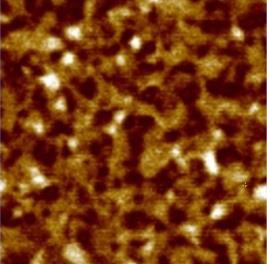
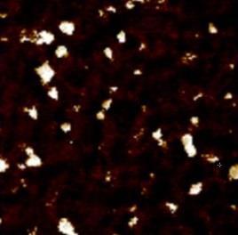
5 5 Imaging & Spectroscopy Tunneling AFM (TUNA) on a carpet of standing carbon nanotubes (1x1 µm scan) Height (nm) Current (pa) I-V Spectra
6 6 Expand the Capability on 3 levels: Capture electrical spectra in every pixel Correlate electrical & mechanical properties Eliminate contact mode limitations, and expand to soft & fragile samples


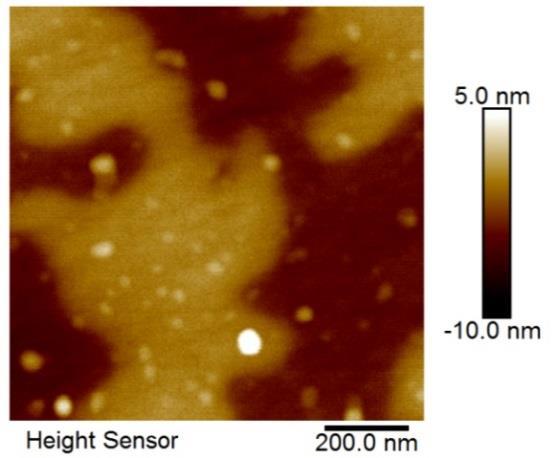
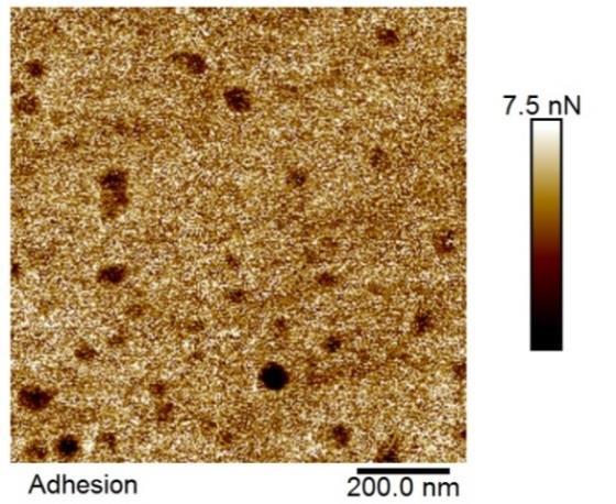
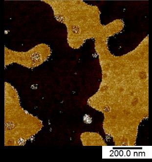
7 7 Expand the Capability on 3 levels: Capture electrical spectra in every pixel Correlate electrical & mechanical properties Eliminate contact mode limitations, and expand to soft & fragile samples PeakForce Tapping PeakForce TUNA on P3HT:CNT blends (700x700 nm scan) Height Adhesion Current Collaboration with Ph. Leclere, Uni Mons, Belgium See also: Nanoscale 4, no. 8 (2012), 2705.
8 8 DataCubes


9 9 DataCubes Electrical Characterization Principle Fast Force Volume imaging: a force-distance spectrum in every pixel Z Force Insert a hold segment (= dwell time ) and perform an electrical measurement during the hold segment: electrical spectrum in every pixel DC Sample Voltage Electrical Channel
 Force-distance")
 TUNA current slices shown as")
10 10 DCUBE-TUNA (Tunneling AFM) on Maghemite (γ-fe 2 O 3 ) Force-distance & I-V spectrum in every pixel (110 ms/pixel) TUNA current slices shown as movie (movie)
 on Maghemite (γ-fe 2")


11 11 DCUBE-TUNA (Tunneling AFM) on Maghemite (γ-fe 2 O 3 ) The datacube can be analyzed as current slice data The datacube can be analyzed as I-V spectra


")


12 12 DataCubes Electrical Characterization Principle Ramp Parameter Output Channel MECHANICAL Force Volume DCUBE-TUNA DCUBE-SSRM DCUBE-SCM DCUBE-sMIM DCUBE-PFM Distance V DC V DC Force Stiffness Adhesion Modulus Current log(resistance) ELECTRICAL V DC V AC f AC Phase dc/dv Amplitude dc/dv Phase V DC V AC f AC Phase dc/dv Amplitude dc/dv Phase smim-c smim-r V DC V AC f AC Phase PFM Amplitude PFM Phase Example Spectra
13 13 Capture electrical spectra in every pixel More information than other electrical AFM modes Access previously inaccessible material properties and device data


14 DCUBE-TUNA (Tunneling AFM) on Maghemite (γ-fe 2 O 3 ) Using Matlab export/import functions, one can perform custom analysis: Here we fit all I-V spectra to extract potential barriers: y = ae bx + ce dx Data processing by N. Chevalier & D. Mariolle at Uni. Grenoble Alpes, CEA, LETI No Conduction (movie) V b+ = ln (a) > 0 b 3/29/2018 Bruker Webinar 14 Ohmic
 Data courtesy: N. Chevalier & D. Mariolle at Uni. Grenoble Alpes, CEA, LETI, France dc/dv Amplitude -1.6V -1.2V -0.8V -0.")
15 15 DCUBE-SCM (Scanning Capacitance Microscopy) on SRAM Transistors Sample voltage ramp from -2V to 2V 128x128 pixels, 2x2 µm scan 100 ms/pixel (27 min/cube) Data courtesy: N. Chevalier & D. Mariolle at Uni. Grenoble Alpes, CEA, LETI, France dc/dv Amplitude -1.6V -1.2V -0.8V -0.4V p n p p n p (movie)

16 DCUBE-SCM (Scanning Capacitance Microscopy) on SRAM Transistors Sample voltage (V DC ) ramp from -2V to 2V in every pixel Slices through the datacube show how the pnp junction profile changes with V DC Data courtesy: N. Chevalier & D. Mariolle at Uni. Grenoble Alpes, CEA, LETI, France slice at fixed V DC dc/dv Amplitude DataCube slice at fixed Y position p n p Y p n p V DC V DC Y X 3/29/2018 Bruker Webinar 16

 on")

 in every")


17 17 DCUBE-sMIM (Microwave Impedance Microscopy) on Doped Si Device C-V and dc/dv-v spectra (-2V to +2V) in every pixel smim-c dc/dv Amplitude dc/dv Phase -2.0V -1.5V -1.0V -0.5V 0.0V 0.5V 1.0V 1.5V 2.0V
 on Si with staircase")


18 18 DCUBE-sMIM (Microwave Impedance Microscopy) on Si with staircase carrier profile Sample voltage ramp from -2V to 2V in every pixel results in C-V spectra Sample source: Infineon Munich, DOI: /j.microrel smim-r vs. time p-type n-type -1V V + + smim-c vs. time
19 19 Practical Aspect: Speed? Typ. time (ms) Force-Distance Spectrum Electrical spectrum Total Mode Bandwidth (khz) TUNA 15 smim 300 SCM 1-10 PFM 1-10 *fac and LIA BW dependent Time per Image (min) Time per pixel 20 ms 100 ms 200 ms 64x Pixels 128x x ms 50 ms 12 ms 100 ms 25 ms smim C-V spectra on Si sample, collected at different speeds


20 20 DCUBE-PFM (Piezoresponse Force Microscopy) on BFO PFM Amplitude and PFM Phase data slices Domains switch as voltage is increased. Different domains switch at different voltages -6V -5V -4V -3V -2V -1V 0V Amplitude Phase
 on BFO")


21 DCUBE-PFM (Piezoresponse Force Microscopy) on BFO Amplitude spectra along one line are shown The images represent the PFM amplitude & phase vs. voltage along the line Sample Bias (V) X -6 X 3/29/2018 Bruker Webinar 21
22 22 Correlate electrical & mechanical properties


 and study differences")


23 DCUBE-TUNA (Tunneling AFM) on Battery Cathode Modulus, Adhesion, Stiffness & conductivity from -4V to +4V The data allow one to identify all elements (Li metal oxide, binder & carbon nanoparticles) and study differences between different metal oxide grains -3.5V -2.5V -1.5V -0.5V +0.25V Li metaloxide +1V +1.75V +2.5V +3.25V +4V Polymer binder Carbon black 3/29/2018 Bruker Webinar 23
 on")


24 24 DCUBE-TUNA (Tunneling AFM) on Battery Cathode +3V -3V Modulus, Adhesion, Stiffness & conductivity from -4V to +4V All I-V spectra in selected area displayed
 on")

 Mechanical")

25 25 DCUBE-sMIM (Microwave Impedance Microscopy) on Maghemite (γ-fe 2 O 3 ) smim-c smim-r During a short hold segment, the DC bias was kept constant (no spectra) Mechanical properties (Adhesion shown) acquired simultaneously smim-c vs. time spectra shown for 5 positions
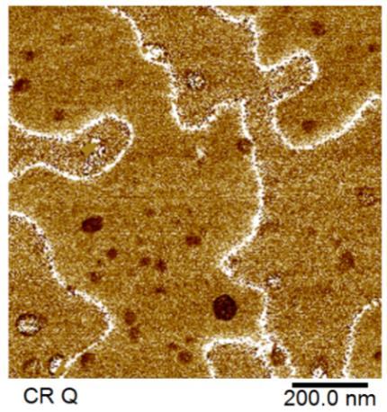


26 26 DCUBE-CR-PFM (Contact Resonance PFM) on LiTaO 3 (movie)
27 27 Eliminate contact mode limitations Longer tip lifetime Characterize soft & fragile samples Better spatial resolution

 on")


28 28 DCUBE-TUNA (Tunneling AFM) on Battery Cathode -4.0V -3.0V -1.0V +1V +2.0V +3.0V +4.0V
 on P3HT")
")
 +3V sample")
29 29 Peakforce-TUNA (Tunneling AFM) on P3HT Organic conductive nanowires Height (nm) Adhesion (nn) Current (pa) +3V sample voltage, 3x3 µm scan


30 30 Summary Combining Fast Force Volume imaging with Electrical modes generates Datacubes enhancing the capabilities of conventional electrical AFM modes: Capture electrical spectra in every pixel Correlate electrical & mechanical properties Eliminate contact mode limitations & expand to soft & fragile samples Height Modulus Current (movie)

31 Copyright Bruker Corporation. All rights reserved.
Cutting-edge Atomic Force Microscopy techniques for large and multiple samples
 Cutting-edge Atomic Force Microscopy techniques for large and multiple samples Study of up to 200 mm samples using the widest set of AFM modes Industrial standards of automation A unique combination of
Rebirth of Force Spectroscopy: Advanced Nanomechanical, Electrical, Optical, Thermal and Piezoresponse Studies
 HybriD Mode Rebirth of Force Spectroscopy: Advanced Nanomechanical, Electrical, Optical, Thermal and Piezoresponse Studies Fast Quantitative Nanomechanical Measurements and Force Volume Simultaneous Electrostatic
Scanning Microwave. Expanding Impedance Measurements to the Nanoscale: Coupling the Power of Scanning Probe Microscopy with the PNA
 Agilent Technologies Scanning Microwave Microscopy (SMM) Expanding Impedance Measurements to the Nanoscale: Coupling the Power of Scanning Probe Microscopy with the PNA Presented by: Craig Wall PhD Product
Asylum Research. MFP-3D Infinity. Endless Applications. Unlimited Potential. Performance / Versatility / Support
 MFP-3D Infinity AFM Asylum Research Endless Applications. Unlimited Potential. Performance / Versatility / Support MFP-3D Infinity AFM Asylum Research Endless applications. Unlimited potential. The Asylum
Keysight Technologies Scanning Microwave Microscopy Solutions for Quantitative Semiconductor Device Characterization.
 Keysight Technologies Scanning Microwave Microscopy Solutions for Quantitative Semiconductor Device Characterization Application Note Introduction The scanning microwave microscope (SMM) merges the nanoscale
INDIAN INSTITUTE OF TECHNOLOGY BOMBAY
 IIT Bombay requests quotations for a high frequency conducting-atomic Force Microscope (c-afm) instrument to be set up as a Central Facility for a wide range of experimental requirements. The instrument
Keysight Technologies Scanning Microwave Microscope Mode. Application Note
 Keysight Technologies Scanning Microwave Microscope Mode Application Note Introduction Measuring electromagnetic properties of materials can provide insight into applications in many areas of science and
Electronic Characterization of Materials Using Conductive AFM
 Electronic Characterization of Materials Using Conductive AFM Amir Moshar Electrical Measurements SKPM EFM CAFM PFM SCM Non-Contact Electrical Techniques Scanning Kelvin Probe Microscopy Electric Force
Options and Accessories for Asylum Research MFP-3D AFMs
 ACCESSORIES Options and Accessories for Asylum Research MFP-3D AFMs Empower your research with powerful, innovative new capabilities Go beyond topography with advanced modes and environmental control Powerful
Mapping piezoelectric response in nanomaterials using a dedicated non-destructive scanning probe technique. Supporting Information
 Electronic Supplementary Material (ESI) for Nanoscale. This journal is The Royal Society of Chemistry 2017 Mapping piezoelectric response in nanomaterials using a dedicated non-destructive scanning probe
; A=4π(2m) 1/2 /h. exp (Fowler Nordheim Eq.) 2 const
 1/2 /h. exp (Fowler Nordheim Eq.) 2 const") Scanning Tunneling Microscopy (STM) Brief background: In 1981, G. Binnig, H. Rohrer, Ch. Gerber and J. Weibel observed vacuum tunneling of electrons between a sharp tip and a platinum surface. The tunnel
Scanning Tunneling Microscopy (STM) Brief background: In 1981, G. Binnig, H. Rohrer, Ch. Gerber and J. Weibel observed vacuum tunneling of electrons between a sharp tip and a platinum surface. The tunnel
Park NX20 The leading nano metrology tool for failure analysis and large sample research.
 The Most Accurate Atomic Force Microscope Park NX20 The leading nano metrology tool for failure analysis and large sample research www.parkafm.com The Most Accurate Atomic Force Microscope Park NX20 The
Keysight Technologies 5500 AFM Controller Upgrade. Data Sheet
 Keysight Technologies 5500 AFM Controller Upgrade Data Sheet 02 Keysight 5500 AFM Controller Upgrade - Data Sheet Upgrade Overview The Keysight 5500 AFM Controller Upgrade offers a tremendously convenient
AFM Probes. Innovation with Integrity. AFM Probes
 AFM Probes 2013 Innovation with Integrity AFM Probes 1 How to Order Americas Order online (USA only): www.brukerafmprobes.com Phone Orders: +1 (800) 715-8440 Option 6 Purchase Order by Fax: +1 (805) 696-6310
Distinguishing Between Mechanical and Electrostatic. Interaction in Single-Pass Multifrequency Electrostatic Force
 SUPPORTING INFORMATION Distinguishing Between Mechanical and Electrostatic Interaction in Single-Pass Multifrequency Electrostatic Force Microscopy on a Molecular Material Marta Riba-Moliner, Narcis Avarvari,
Measurement of Microscopic Three-dimensional Profiles with High Accuracy and Simple Operation
 238 Hitachi Review Vol. 65 (2016), No. 7 Featured Articles Measurement of Microscopic Three-dimensional Profiles with High Accuracy and Simple Operation AFM5500M Scanning Probe Microscope Satoshi Hasumura
NAME: Last First Signature
 UNIVERSITY OF CALIFORNIA, BERKELEY College of Engineering Department of Electrical Engineering and Computer Sciences EE 130: IC Devices Spring 2003 FINAL EXAMINATION NAME: Last First Signature STUDENT
Agilent Technologies Gli analizzatori di reti della serie-x
 Agilent Technologies Gli analizzatori di reti della serie-x Luigi Fratini 1 Introducing the PNA-X Performance Network Analyzer For Active Device Test 500 GHz & beyond! 325 GHz 110 GHz 67 GHz 50 GHz 43.5
Microscopic Structures
 Microscopic Structures Image Analysis Metal, 3D Image (Red-Green) The microscopic methods range from dark field / bright field microscopy through polarisation- and inverse microscopy to techniques like
Dual-channel Lock-in Amplifier Module
 Dual-channel Lock-in Amplifier Module Introduction Phase-locked amplification and demodulation techniques of weak signals have a wide range of applications in Turnable Diode Laser Absorption Spectrum (TDLAS)
AFM Lab Aplication note P01. AD8429 Piezoresponse Force Microscopy Amplifier
 AD8429 Piezoresponse Force Microscopy Amplifier - New standard for PFM measurements - State of the art signal amplifier - Designed and built in AFM Lab - Compatible with PFM,EFM,MFM Based in the Analog
Supplementary Materials for
 advances.sciencemag.org/cgi/content/full/4/2/e1700324/dc1 Supplementary Materials for Photocarrier generation from interlayer charge-transfer transitions in WS2-graphene heterostructures Long Yuan, Ting-Fung
Nanoscale Material Characterization with Differential Interferometric Atomic Force Microscopy
 Nanoscale Material Characterization with Differential Interferometric Atomic Force Microscopy F. Sarioglu, M. Liu, K. Vijayraghavan, A. Gellineau, O. Solgaard E. L. Ginzton Laboratory University Tip-sample
Supplementary Materials for
 advances.sciencemag.org/cgi/content/full/2/7/e1629/dc1 Supplementary Materials for Subatomic deformation driven by vertical piezoelectricity from CdS ultrathin films Xuewen Wang, Xuexia He, Hongfei Zhu,
Scanning Tunneling Microscopy
 Scanning Tunneling Microscopy The wavelike properties of electrons allows them to tunnel beyond the regions of a solid into a region of space forbidden for them to exist in. In this region they can be
Scanning Tunneling Microscopy
 EMSE-515 02 Scanning Tunneling Microscopy EMSE-515 F. Ernst 1 Scanning Tunneling Microscope: Working Principle 2 Scanning Tunneling Microscope: Construction Principle 1 sample 2 sample holder 3 clamps
Department of Electrical Engineering IIT Madras
 Department of Electrical Engineering IIT Madras Sample Questions on Semiconductor Devices EE3 applicants who are interested to pursue their research in microelectronics devices area (fabrication and/or
photolithographic techniques (1). Molybdenum electrodes (50 nm thick) are deposited by
. Molybdenum electrodes (50 nm thick) are deposited by") Supporting online material Materials and Methods Single-walled carbon nanotube (SWNT) devices are fabricated using standard photolithographic techniques (1). Molybdenum electrodes (50 nm thick) are deposited
Supporting online material Materials and Methods Single-walled carbon nanotube (SWNT) devices are fabricated using standard photolithographic techniques (1). Molybdenum electrodes (50 nm thick) are deposited
Park XE7 The most affordable research grade AFM with flexible sample handling.
 Park XE7 The most affordable research grade AFM with flexible sample handling www.parkafm.com Park Systems The Most Accurate Atomic Force Microscope Park XE7 The economical choice for innovative research
Advanced Nanoscale Metrology with AFM
 Advanced Nanoscale Metrology with AFM Sang-il Park Corp. SPM: the Key to the Nano World Initiated by the invention of STM in 1982. By G. Binnig, H. Rohrer, Ch. Gerber at IBM Zürich. Expanded by the invention
Expanding Impedance Measurement to Nanoscale:
 Expanding Impedance Measurement to Nanoscale: Coupling the Power of Scanning Probe Microscopy with Performance Network Analyzer (PNA) Hassan Tanbakuchi Senior Research Scientist Agilent Technologies Agilent
- Near Field Scanning Optical Microscopy - Electrostatic Force Microscopy - Magnetic Force Microscopy
 - Near Field Scanning Optical Microscopy - Electrostatic Force Microscopy - Magnetic Force Microscopy Yongho Seo Near-field Photonics Group Leader Wonho Jhe Director School of Physics and Center for Near-field
Lateral Force: F L = k L * x
 Scanning Force Microscopy (SFM): Conventional SFM Application: Topography measurements Force: F N = k N * k N Ppring constant: Spring deflection: Pieo Scanner Interaction or force dampening field Contact
Fine structure of the inner electric field in semiconductor laser diodes studied by EFM.
 Fine structure of the inner electric field in semiconductor laser diodes studied by EFM. Phys. Low-Dim. Struct. 3/4, 9 (2001). A.Ankudinov 1, V.Marushchak 1, A.Titkov 1, V.Evtikhiev 1, E.Kotelnikov 1,
Supporting Information
 Strength of recluse spider s silk originates from nanofibrils Supporting Information Qijue Wang, Hannes C. Schniepp* Applied Science Department, The College of William & Mary, P.O. Box 8795, Williamsburg,
Suivie de résonance: méthodes à fréquences multiples. Romain Stomp Application Scientist, Zurich Instruments AG. ZI Applications
 Suivie de résonance: méthodes à fréquences multiples Romain Stomp Application Scientist, Zurich Instruments AG Slide 1 Sommaire 1. Un peu de traitement du signal pour le SPM Détection synchrone pour le
Electrical Properties of Chicken Herpes Virus Based on Impedance Analysis using Atomic Force Microscopy
 Electrical Properties of Chicken Herpes Virus Based on Impedance Analysis using Atomic Force Microscopy Zhuxin Dong Ph. D. Candidate, Mechanical Engineering University of Arkansas Brock Schulte Masters
January, 2004 Jeju Island. Acknowledgements OTFL
 High-Speed Fabrication of Nanostructures using Atomic Force Microscope Lithography Haiwon Lee Department of Chemistry US-Korea NanoForum 02/17, 2005 January, 2004 Jeju Island Acknowledgements Contents
Radio-frequency scanning tunneling microscopy
 doi: 10.1038/nature06238 SUPPLEMENARY INFORMAION Radio-frequency scanning tunneling microscopy U. Kemiktarak 1,. Ndukum 2, K.C. Schwab 2, K.L. Ekinci 3 1 Department of Physics, Boston University, Boston,
LOW TEMPERATURE STM/AFM
 * CreaTec STM of Au(111) using a CO-terminated tip, 20mV bias, 0.6nA* LOW TEMPERATURE STM/AFM High end atomic imaging, spectroscopy and manipulation Designed and manufactured in Germany by CreaTec Fischer
High-Speed Scalable Silicon-MoS 2 P-N Heterojunction Photodetectors
 High-Speed Scalable Silicon-MoS 2 P-N Heterojunction Photodetectors Veerendra Dhyani 1, and Samaresh Das 1* 1 Centre for Applied Research in Electronics, Indian Institute of Technology Delhi, New Delhi-110016,
SPM The Industry s Performance Leader High Resolution Closed-loop System Fast, Easy Tip & Sample Exchange Versatility and Value Powerful Research
 SPM The Industry s Performance Leader High Resolution Closed-loop System Fast, Easy Tip & Sample Exchange Versatility and Value Powerful Research Flexibility Atomic resolution STM image of highly-oriented
Manufacturing Metrology Team
 The Team has a range of state-of-the-art equipment for the measurement of surface texture and form. We are happy to discuss potential measurement issues and collaborative research Manufacturing Metrology
IMAGING P-N JUNCTIONS BY SCANNING NEAR-FIELD OPTICAL, ATOMIC FORCE AND ELECTRICAL CONTRAST MICROSCOPY. G. Tallarida Laboratorio MDM-INFM
 Laboratorio MDM - INFM Via C.Olivetti 2, I-20041 Agrate Brianza (MI) M D M Materiali e Dispositivi per la Microelettronica IMAGING P-N JUNCTIONS BY SCANNING NEAR-FIELD OPTICAL, ATOMIC FORCE AND ELECTRICAL
Lecture 20: Optical Tools for MEMS Imaging
 MECH 466 Microelectromechanical Systems University of Victoria Dept. of Mechanical Engineering Lecture 20: Optical Tools for MEMS Imaging 1 Overview Optical Microscopes Video Microscopes Scanning Electron
Akiyama-Probe (A-Probe) guide
 guide") Akiyama-Probe (A-Probe) guide This guide presents: what is Akiyama-Probe, how it works, and what you can do Dynamic mode AFM Version: 2.0 Introduction NANOSENSORS Akiyama-Probe (A-Probe) is a self-sensing
Akiyama-Probe (A-Probe) guide This guide presents: what is Akiyama-Probe, how it works, and what you can do Dynamic mode AFM Version: 2.0 Introduction NANOSENSORS Akiyama-Probe (A-Probe) is a self-sensing
Figure for the aim4np Report
 Figure for the aim4np Report This file contains the figures to which reference is made in the text submitted to SESAM. There is one page per figure. At the beginning of the document, there is the front-page
Atomic Force Microscopes
 Nanoscale Surface Characterization tomic Force Microscopes www.witec.de WITec tomic Force Microscopes Nanoscale Surface Characterization The WITec tomic Force Microscope (FM) module integrated with a research-grade
PIEZO FORCE MICROSCOPY AND PEAKFORCE TUNA MEASUREMENTS OF III-V SEMICONDUCTOR NANOWIRES
 LAPPEENRANTA UNIVERSITY OF TECHNOLOGY Faculty of Technology Double Degree Programme in Technical Physics Anatoly Fominykh PIEZO FORCE MICROSCOPY AND PEAKFORCE TUNA MEASUREMENTS OF III-V SEMICONDUCTOR NANOWIRES
Imaging and Spectroscopy Applications Guide
 SPM Applications Guide USER GUIDE 3 Imaging and Spectroscopy Applications Guide User Guide including beta (complete, reviewed) chapters, including draft (nearly complete, not reviewed) chapters, Versionα,
Outline: Introduction: What is SPM, history STM AFM Image treatment Advanced SPM techniques Applications in semiconductor research and industry
 1 Outline: Introduction: What is SPM, history STM AFM Image treatment Advanced SPM techniques Applications in semiconductor research and industry 2 Back to our solutions: The main problem: How to get nm
Keysight Technologies 9500 AFM. Data Sheet
 Keysight Technologies 9500 AFM Data Sheet System Overview The Keysight Technologies, Inc. 9500 AFM seamlessly integrates revolutionary new software, a new high-bandwidth digital controller, and a state-of-the-art
Optical Microscope. Active anti-vibration table. Mechanical Head. Computer and Software. Acoustic/Electrical Shield Enclosure
 Optical Microscope On-axis optical view with max. X magnification Motorized zoom and focus Max Field of view: mm x mm (depends on zoom) Resolution : um Working Distance : mm Magnification : max. X Zoom
The Most Accurate Atomic Force Microscope. Park NX20 The leading nano metrology tool for failure analysis and large sample research.
 The Most Accurate Atomic Force Microscope Park NX20 The leading nano metrology tool for failure analysis and large sample research www.parkafm.com Park Systems The Most Accurate Atomic Force Microscope
Akiyama-Probe (A-Probe) technical guide This technical guide presents: how to make a proper setup for operation of Akiyama-Probe.
 technical guide This technical guide presents: how to make a proper setup for operation of Akiyama-Probe.") Akiyama-Probe (A-Probe) technical guide This technical guide presents: how to make a proper setup for operation of Akiyama-Probe. Version: 2.0 Introduction To benefit from the advantages of Akiyama-Probe,
Akiyama-Probe (A-Probe) technical guide This technical guide presents: how to make a proper setup for operation of Akiyama-Probe. Version: 2.0 Introduction To benefit from the advantages of Akiyama-Probe,
I-V, C-V and AC Impedance Techniques and Characterizations of Photovoltaic Cells
 I-V, C-V and AC Impedance Techniques and Characterizations of Photovoltaic Cells John Harper 1, Xin-dong Wang 2 1 AMETEK Advanced Measurement Technology, Southwood Business Park, Hampshire,GU14 NR,United
Atomic Force Microscopy (Bruker MultiMode Nanoscope IIIA)
") Atomic Force Microscopy (Bruker MultiMode Nanoscope IIIA) This operating procedure intends to provide guidance for general measurements with the AFM. For more advanced measurements or measurements with
Atomic Force Microscopy (Bruker MultiMode Nanoscope IIIA) This operating procedure intends to provide guidance for general measurements with the AFM. For more advanced measurements or measurements with
PFM Experiments with High Voltage DC/AC Bias
 PFM Experiments with High Voltage DC/AC Bias Support Note Shijie Wu and John Alexander Agilent Technologies Introduction Piezoelectric force microscopy (PFM) has found major applications in the study of
Akiyama-Probe (A-Probe) guide
 guide") Akiyama-Probe (A-Probe) guide This guide presents: what is Akiyama-Probe, how it works, and its performance. Akiyama-Probe is a patented technology. Version: 2009-03-23 Introduction NANOSENSORS Akiyama-Probe
Akiyama-Probe (A-Probe) guide This guide presents: what is Akiyama-Probe, how it works, and its performance. Akiyama-Probe is a patented technology. Version: 2009-03-23 Introduction NANOSENSORS Akiyama-Probe
Supporting Online Material for
 www.sciencemag.org/cgi/content/full/31/5771/4/dc1 Supporting Online Material for Piezoelectric Nanogenerators Based on Zinc Oxide Nanowire Arras Zhong in Wang* and Jinhui Song *To whom correspondence should
NanoFocus Inc. Next Generation Scanning Probe Technology. Tel : Fax:
 NanoFocus Inc. Next Generation Scanning Probe Technology www.nanofocus.kr Tel : 82-2-864-3955 Fax: 82-2-864-3956 Albatross SPM is Multi functional research grade system Flexure scanner and closed-loop
Objective Type Questions 1. Why pure semiconductors are insulators at 0 o K? 2. What is effect of temperature on barrier voltage? 3.
 Objective Type Questions 1. Why pure semiconductors are insulators at 0 o K? 2. What is effect of temperature on barrier voltage? 3. What is difference between electron and hole? 4. Why electrons have
PeakForce SECM with Bio-Logic SP-300 Potentiostat
 PeakForce SECM with Bio-Logic SP-300 Potentiostat Weilai Yu (Caltech) 2018.12.29 Preliminaries: 1. To use a Bio-Logic bipotentiostat in place of a CHI760E, follow the Bruker PeakForce SECM manual for all
Nanomechanical Mapping of a High Curvature Polymer Brush Grafted
 Supplementary Information Nanomechanical Mapping of a High Curvature Polymer Brush Grafted from a Rigid Nanoparticle Gunnar Dunér 1, Esben Thormann 1, Andra Dėdinaitė 1,2, Per M. Claesson 1,2, Krzysztof
Rudolf C. Hoffmann, Mareiki Kaloumenos, Silvio Heinschke, Peter Jakes, Emre Erdem Rüdiger-A. Eichel, and Jörg J. Schneider *,
 Molecular precursor derived and solution processed indium zinc oxide as semiconductor in a field-effect transistor device. Towards an improved understanding of semiconductor film composition. Rudolf C.
QUESTION BANK EC6201 ELECTRONIC DEVICES UNIT I SEMICONDUCTOR DIODE PART A. It has two types. 1. Intrinsic semiconductor 2. Extrinsic semiconductor.
 FATIMA MICHAEL COLLEGE OF ENGINEERING & TECHNOLOGY Senkottai Village, Madurai Sivagangai Main Road, Madurai - 625 020. [An ISO 9001:2008 Certified Institution] QUESTION BANK EC6201 ELECTRONIC DEVICES SEMESTER:
Keysight Technologies Using Non-Contact AFM to Image Liquid Topographies. Application Note
 Keysight Technologies Using Non-Contact AFM to Image Liquid Topographies Application Note Introduction High resolution images of patterned liquid surfaces have been acquired without inducing either capillary
An advanced impedance calibration method for nanoscale microwave imaging
 An advanced impedance calibration method for nanoscale microwave imaging M. Kasper 1, *, G. Gramse 2 and F. Kienberger 1 1 Keysight Technologies Austria GmbH, Keysight Labs, Gruberstrasse 40, 4020 Linz,
MEMS for RF, Micro Optics and Scanning Probe Nanotechnology Applications
 MEMS for RF, Micro Optics and Scanning Probe Nanotechnology Applications Part I: RF Applications Introductions and Motivations What are RF MEMS? Example Devices RFIC RFIC consists of Active components
The Most Accurate Atomic Force Microscope. Park XE15 Power and versatility, brilliantly combined.
 The Most Accurate Atomic Force Microscope Park XE15 Power and versatility, brilliantly combined. www.parkafm.com Park XE15 Increase your productivity with our powerfully versatile atomic force microscope
Lecture 18: Photodetectors
 Lecture 18: Photodetectors Contents 1 Introduction 1 2 Photodetector principle 2 3 Photoconductor 4 4 Photodiodes 6 4.1 Heterojunction photodiode.................... 8 4.2 Metal-semiconductor photodiode................
SUPPLEMENTARY INFORMATION
 SUPPLEMENTARY INFORMATION Dopant profiling and surface analysis of silicon nanowires using capacitance-voltage measurements Erik C. Garnett 1, Yu-Chih Tseng 4, Devesh Khanal 2,3, Junqiao Wu 2,3, Jeffrey
Investigating the Electronic Behavior of Nano-materials From Charge Transport Properties to System Response
 Investigating the Electronic Behavior of Nano-materials From Charge Transport Properties to System Response Amit Verma Assistant Professor Department of Electrical Engineering & Computer Science Texas
Atomic-layer deposition of ultrathin gate dielectrics and Si new functional devices
 Atomic-layer deposition of ultrathin gate dielectrics and Si new functional devices Anri Nakajima Research Center for Nanodevices and Systems, Hiroshima University 1-4-2 Kagamiyama, Higashi-Hiroshima,
Keysight 9500 AFM. Data Sheet
 Keysight 9500 AFM Data Sheet System Overview The Keysight Technologies, Inc. 9500 AFM seamlessly integrates revolutionary new software, a new high-bandwidth digital controller, and a state-of-the-art mechanical
techniques, and gold metalization in the fabrication of this device.
 Up to 6 GHz Medium Power Silicon Bipolar Transistor Chip Technical Data AT-42 Features High Output Power: 21. dbm Typical P 1 db at 2. GHz 2.5 dbm Typical P 1 db at 4. GHz High Gain at 1 db Compression:
Supporting Information. Atomic-scale Spectroscopy of Gated Monolayer MoS 2
 Height (nm) Supporting Information Atomic-scale Spectroscopy of Gated Monolayer MoS 2 Xiaodong Zhou 1, Kibum Kang 2, Saien Xie 2, Ali Dadgar 1, Nicholas R. Monahan 3, X.-Y. Zhu 3, Jiwoong Park 2, and Abhay
I-V, C-V and Impedance Characterization of Photovoltaic Cells using Solartron Instrumentation
 MTSAP1 I-V, C-V and Impedance Characterization of Photovoltaic Cells using Solartron Instrumentation Introduction Harnessing energy from the sun offers an alternative to fossil fuels. Photovoltaic cells
DEVELOPMENT OF A SILICON NANOWIRE MASK USING SCANNING PROBE MICROSCOPY. A Thesis. presented to
 DEVELOPMENT OF A SILICON NANOWIRE MASK USING SCANNING PROBE MICROSCOPY A Thesis presented to the Faculty of the California Polytechnic State University, San Luis Obispo In Partial Fulfillment of the Requirements
Up to 6 GHz Low Noise Silicon Bipolar Transistor Chip. Technical Data AT-41400
 Up to 6 GHz Low Noise Silicon Bipolar Transistor Chip Technical Data AT-1 Features Low Noise Figure: 1.6 db Typical at 3. db Typical at. GHz High Associated Gain: 1.5 db Typical at 1.5 db Typical at. GHz
Nanonics Systems are the Only SPMs that Allow for On-line Integration with Standard MicroRaman Geometries
 Nanonics Systems are the Only SPMs that Allow for On-line Integration with Standard MicroRaman Geometries 2002 Photonics Circle of Excellence Award PLC Ltd, England, a premier provider of Raman microspectral
Radio-Frequency Circuits Integration Using CMOS SOI 0.25µm Technology
 Radio-Frequency Circuits Integration Using CMOS SOI.5µm Technology Frederic Hameau and Olivier Rozeau CEA/LETI - 7, rue des Martyrs -F-3854 GRENOBLE FRANCE cedex 9 frederic.hameau@cea.fr olivier.rozeau@cea.fr
RHK Technology. Application Note: Kelvin Probe Force Microscopy with the RHK R9. ω mod allows to fully nullify any contact potential difference
 Peter Milde 1 and Steffen Porthun 2 1-Institut für Angewandte Photophysik, TU Dresden, D-01069 Dresden, Germany 2-RHK Technology, Inc. Introduction Kelvin-probe force microscopy (KPFM) is an operation
Chihyun Hwang, Tae-Hee Kim, Yoon-Gyo Cho, Jieun Kim and Hyun-Kon Song*
 Supporting Information All-in-one assembly based on 3D-intertangled and cross-jointed architectures of Si/Cu 1D-nanowires for lithium ion batteries Chihyun Hwang, Tae-Hee Kim, Yoon-Gyo Cho, Jieun Kim and
Long-distance propagation of short-wavelength spin waves. Liu et al.
 Long-distance propagation of short-wavelength spin waves Liu et al. Supplementary Note 1. Characterization of the YIG thin film Supplementary fig. 1 shows the characterization of the 20-nm-thick YIG film
Ionscope SICM. About Ionscope. Scanning Ion Conductance Microscopy. Ionscope A brand of Openiolabs Limited
 SICM About is a brand of openiolabs Ltd, headquartered in Cambridge UK, is the world-leader in (SICM), a rapidly emerging Scanning Probe Microscopy (SPM) technique which allows nanoscale topographical
SUPPLEMENTARY INFORMATION
 SUPPLEMENTARY INFORMATION doi:10.1038/nature11293 1. Formation of (111)B polar surface on Si(111) for selective-area growth of InGaAs nanowires on Si. Conventional III-V nanowires (NWs) tend to grow in
Supporting Information
 Solution-processed Nickel Oxide Hole Injection/Transport Layers for Efficient Solution-processed Organic Light- Emitting Diodes Supporting Information 1. C 1s high resolution X-ray Photoemission Spectroscopy
Fundamentals of CMOS Image Sensors
 CHAPTER 2 Fundamentals of CMOS Image Sensors Mixed-Signal IC Design for Image Sensor 2-1 Outline Photoelectric Effect Photodetectors CMOS Image Sensor(CIS) Array Architecture CIS Peripherals Design Considerations
Compact EUV Source for Metrology and Inspection
 Compact EUV Source for Metrology and Inspection Klaus Bergmann, Jochen Vieker, Alexander von Wezyk 2015 EUV Source Workshop, 10.11.2015, Dublin Overview Introduction Xenon based EUV Source FS5420 Consideration
Semiconductor Detector Systems
 Semiconductor Detector Systems Helmuth Spieler Physics Division, Lawrence Berkeley National Laboratory OXFORD UNIVERSITY PRESS ix CONTENTS 1 Detector systems overview 1 1.1 Sensor 2 1.2 Preamplifier 3
Basic Electronics. Introductory Lecture Course for. Technology and Instrumentation in Particle Physics Chicago, Illinois June 9-14, 2011
 Basic Electronics Introductory Lecture Course for Technology and Instrumentation in Particle Physics 2011 Chicago, Illinois June 9-14, 2011 Presented By Gary Drake Argonne National Laboratory Session 3
Depletion width measurement in an organic Schottky contact using a Metal-
 Depletion width measurement in an organic Schottky contact using a Metal- Semiconductor Field-Effect Transistor Arash Takshi, Alexandros Dimopoulos and John D. Madden Department of Electrical and Computer
Author(s) Issue Date Text Version author. DOI / /18/9/095501
 Issue Date Text Version author. DOI / /18/9/095501") Title Author(s) Citation Refinement of Conditions of Point-Contact Current Imaging Atomic Force Microscopy for Molecular-Scale Conduction Measurements Yajima, Takashi; Tanaka, Hirofumi; Matsumoto, Takuya;
Title Author(s) Citation Refinement of Conditions of Point-Contact Current Imaging Atomic Force Microscopy for Molecular-Scale Conduction Measurements Yajima, Takashi; Tanaka, Hirofumi; Matsumoto, Takuya;
NOISE IN MEMS PIEZORESISTIVE CANTILEVER
 NOISE IN MEMS PIEZORESISTIVE CANTILEVER Udit Narayan Bera Mechatronics, IIITDM Jabalpur, (India) ABSTRACT Though pezoresistive cantilevers are very popular for various reasons, they are prone to noise
Graphene electro-optic modulator with 30 GHz bandwidth
 Graphene electro-optic modulator with 30 GHz bandwidth Christopher T. Phare 1, Yoon-Ho Daniel Lee 1, Jaime Cardenas 1, and Michal Lipson 1,2,* 1School of Electrical and Computer Engineering, Cornell University,
Characterisation of Photovoltaic Materials and Cells
 Standard Measurement Services and Prices No. Measurement Description Reference 1 Large area, 0.35-sun biased spectral response (SR) 2 Determination of linearity of spectral response with respect to irradiance
A scanning tunneling microscopy based potentiometry technique and its application to the local sensing of the spin Hall effect
 A scanning tunneling microscopy based potentiometry technique and its application to the local sensing of the spin Hall effect Ting Xie 1, a), Michael Dreyer 2, David Bowen 3, Dan Hinkel 3, R. E. Butera
R9 SPM Control System
 R9 SPM Control System Explore with Confidence 5 R9 SPM Control System Explore with Confidence The Technological Legacy of RHK RHK s revolutionary R9 is built on the heritage of over 5 years of technological
SUPPLEMENTARY INFORMATION
 Figure S. Experimental set-up www.nature.com/nature Figure S2. Dependence of ESR frequencies (GHz) on a magnetic field (G) applied in different directions with respect to NV axis ( θ 2π). The angle with