QUESTION BANK B.TECH (IV YEAR I SEM) ( )
|
|
|
- Roy Harrell
- 5 years ago
- Views:
Transcription
 Recognized under 2(f) and 12 (B) of UGC ACT 1956 (Affiliated to JNTUH, Hyderabad, Approved by AICTE - Accredited by NBA & NAAC A Grade - ISO 9001:2015 Certified) Maisammaguda, Dhulapally")
1 QUESTION BANK B.TECH (IV YEAR I SEM) ( ) Department of Electronics & Communication Engineering MALLA REDDY COLLEGE OF ENGINEERING & TECHNOLOGY (Autonomous Institution UGC, Govt. of India) Recognized under 2(f) and 12 (B) of UGC ACT 1956 (Affiliated to JNTUH, Hyderabad, Approved by AICTE - Accredited by NBA & NAAC A Grade - ISO 9001:2015 Certified) Maisammaguda, Dhulapally (Post Via. Kompally), Secunderabad , Telangana State, India
2 Code No: RT41041 R13 Set No. 1 IV B.Tech I Semester Supplementary Examinations, February/March VLSI DESIGN (Common to Electronics and Communication Engineering and Electronics and Instrumentation Engineering) Time: 3 hours Max. Marks: 70 Question paper consists of Part-A and Part-B Answer ALL sub questions from Part-A Answer any THREE questions from Part-B ***** PART A (22 Marks) 1. a) When the channel is said to be pinched off? [3] b) What are the different MOS layers? [4] c) Give the different scaling models and scaling factors? [3] d) State the disadvantages of dynamic CMOS logic? [4] e) What are the different levels of design abstraction at physical design? [4] f) What information from the targeted FPGA device is required in RTL synthesis? [4] PART B (3x16 = 48 Marks) 2. a) With neat sketches explain the CMOS n-well fabrication process indicating the masks used. [8] b) What is threshold voltage of a MOS device and explain its significance. [8] 3. a) Discuss CMOS design style. Compare with nmos design style? [8] b) Design a stick diagram for two input nmos NAND and NOR gates? [8] 4. a) Why scaling is required? Write the scaling factors for different types of device parameters? [8] b) Discuss the limits due to sub threshold currents. [8] 5. a) Describe constructional features and performance characteristic of Pseudo- NMOS logic. [8] b) Explain two-phase clock generator using D flip-flops and draw the corresponding waveforms. [8] 6. a) Write down the comparisons between Field Programmable Gate Array and Application Specific Integrated Circuit in detail. [8] b) Give the steps in ASIC design flow with flow diagram and briefly discuss about each step. [8] 7. a) Write down the step by step approach of FPGA design process on XILINX environment? [8] b) Design a queue and write the dataflow style VHDL program for the same. [8] 1 of 1
3 Code No: RT41041 R13 Set No. 1 IV B.Tech I Semester Regular/Supplementary Examinations, October/November VLSI DESIGN (Common to Electronics and Communication Engineering and Electronics and Instrumentation Engineering) Time: 3 hours Max. Marks: 70 Question paper consists of Part-A and Part-B Answer ALL sub questions from Part-A Answer any THREE questions from Part-B ***** PART A (22 Marks) 1. a) Clearly explain about ION-IMPLANTATION step in IC fabrication. [4] b) Why is VLSI design process presented in NMOS only? Justify with an example? [4] c) Explain the formal estimation of CMOS Inverter delay. [4] d) Write a short note on clocked sequential circuits. [3] e) Write a short note on clock mechanisms in VLSI design. [4] f) List out the applications of FPGAs. [3] PART B (3x16 = 48 Marks) 2. a) Compare CMOS and Bipolar technologies. [8] b) Explain the NMOS fabrication procedure. [8] 3. a) Illustrate the lambda-based design rules with neat sketches. [8] b) Design an area efficient layout diagram for the CMOS logic shown below Y = (A + B + C). [8] 4. a) What is meant by sheet resistance Rs? Explain the concept of Rs applied to MOS transistors. [8] b) Calculate on resistance of an inverter from VDD to GND. If n- channel sheet resistance Rsn=10 4 Ω per square and P-channel sheet resistance Rsp = Ω per square.(zpu=4:4 and Zpd=2:2). [8] 5. a) Give the subsystem design considerations of a four-bit adder. [8] b) Explain step-by-step subsystem design approach. Consider an example. [8] 6. a) Explain the terms (i) Static power dissipation (ii) Dynamic power dissipation. [8] b) Discuss the VLSI design issues and design trends. [8] 7. a) Write about FPGA Programming Technologies in detail. [8] b) Explain the step by step approach of FPGA design process on Xilinx [8] environment. '' ''' '' ''' 1 of 1
4 Code No: RT41041 R13 Set No. 2 IV B.Tech I Semester Regular/Supplementary Examinations, October/November VLSI DESIGN (Common to Electronics and Communication Engineering and Electronics and Instrumentation Engineering) Time: 3 hours Max. Marks: 70 Question paper consists of Part-A and Part-B Answer ALL sub questions from Part-A Answer any THREE questions from Part-B ***** PART A (22 Marks) 1. a) Define threshold voltage of a MOS device and explain its significance. [4] b) Discuss different forms of pull up, mentioning merits and demerits of each form. [4] c) What is meant by standard unit of capacitance? Give some area capacitance calculations. [4] d) Draw and explain fan-in and fan-out characteristics of different CMOS design Technologies. [4] e) Give two reasons about the importance of package selection in VLSI design. [3] f) Write a short notes on FPGA configuration and configuration modes. [3] PART B (3x16 = 48 Marks) 2. a) Derive an equation for I DS of an n-channel Enhancement MOSFET operating in Saturation region. [8] b) An nmos transistor is operating in saturation region with the following parameters. VGS = 5V ; Vtn = 1.2V ; W/L = 110; μncox = 110 μa/v 2. Find Transconductance of the device. [8] 3. a) Write a short note on 2μm Double Metal, Double Poly, CMOS/BiCMOS rules. [8] b) Draw the circuit diagrams and the corresponding stick diagrams for nmos and CMOS inverters. [8] 4. a) What are the alternate gate circuits are available? Explain any one of item with suitable sketch. [8] b) Implement the realization of gates using NMOS and PMOS. [8] 5. a) Describe the nature of a parity generator and explain its structured design approach. [8] b) Draw and give the design approach for a carry look ahead adder with its structure. [8] 6. a) Write and explain about the sources of power dissipation in VLSI Design. [8] b) Explain in detail about ASIC design flow with neat sketch. [8] 7. a) Draw and explain the routing architecture of field programmable gate arrays. [8] b) Write about the shift register design and implementation onto FPGA. [8] '' ''' '' ''' 1 of 1
5 Code No: RT41041 R13 Set No. 3 IV B.Tech I Semester Regular/Supplementary Examinations, October/November VLSI DESIGN (Common to Electronics and Communication Engineering and Electronics and Instrumentation Engineering) Time: 3 hours Max. Marks: 70 Question paper consists of Part-A and Part-B Answer ALL sub questions from Part-A Answer any THREE questions from Part-B ***** PART A (22 Marks) 1. a) With neat sketch, explain drain characteristics of an n-channel enhancement MOSFET. [4] b) Compare and contrast the Lambda based and Micron based Rules for layout design. [4] c) Draw and explain the schematic of Pseudo-nMOS Inverter. [3] d) Explain the concept of driving large capacitive loads with, relevant examples. [4] e) List out the back-end steps in ASIC design flow. [3] f) Write about Programmable I/O blocks in FPGAs. [4] PART B (3x16 = 48 Marks) 2. a) With neat sketch explain BICMOS fabrication in an n-well process. [8] b) Explain the term aspects of MOSFET in VLSI Design. [8] 3. a) Tabulate the encoding scheme for a simple single metal CMOS/Bi-CMOS process with respect to various MOS layers. [8] b) Draw the symbolic layout for the CMOS inverter and write the general CMOS logic gate layout guidelines. [8] 4. a) Discuss the inverter delay and propagation delay. [8] b) Write about the scaling limitations due to sub Supply voltages in MOSFETS. [8] 5. a) Explain the architectural issues of subsystem design. [8] b) Explain the structural design approach with an example. [8] 6. a) What is the need of testability? Explain design for testability. [8] b) Explain about SoC design. [8] 7. a) Describe the shift register implementation using VHDL. [8] b) Explain about different programmable elements in FPGA architectures. [8] '' ''' '' ''' 1 of 1
6 Code No: RT41041 R13 Set No. 4 IV B.Tech I Semester Regular/Supplementary Examinations, October/November VLSI DESIGN (Common to Electronics and Communication Engineering and Electronics and Instrumentation Engineering) Time: 3 hours Max. Marks: 70 Question paper consists of Part-A and Part-B Answer ALL sub questions from Part-A Answer any THREE questions from Part-B ***** PART A (22 Marks) 1. a) Explain various regions of CMOS inverter transfer characteristics. [3] b) Write a short note MOS layers and symbolic diagram translation to MASK form. [4] c) Define and give the expressions for any four scaling factors of MOS device parameters. [4] d) Write about general considerations in subsystem design processes. [4] e) Write about technology options in VLSI design. [3] f) Explain the need for FPGA and its applications. [4] PART B (3x16 = 48 Marks) 2. a) Explain different forms of pull-ups used as load in CMOS enhancement. [8] b) Determine pull-up to pull-down ratio of an NMOS inverter when driven through one or more pass transistors. [8] 3. a) Tabulate the encoding scheme for a simple single metal nmos process with respect to various MOS layers. [8] b) What is stick diagram and explain about different symbols used for components in Stick diagram. Draw the stick and layout for a two input CMOS NAND gate. [8] 4. a) Describe three sources of wiring capacitances. Explain the effect of wiring capacitance on the performance of a VLSI circuit. [8] b) Write about the scaling limitations due to sub threshold currents in MOSFETS. [8] 5. Realize the 2-i/p NAND gate using NMOS, PMOS and CMOS technologies. [16] 6. a) Discuss the design flow of system on chip design with neat sketch. [8] b) Explain the steps of specification and logic design in ASIC design flow. [8] 7. a) Write the steps involved to prototype the HDL code onto FPGA device. [10] b) List out the salient features of Xilinx 3000 CLB. [6] 1 of 1 '' ''' '' '''
7 Code No: RT41041 R13 Set No. 1 IV B.Tech I Semester Supplementary Examinations, March VLSI DESIGN (Common to Electronics & Communication Engineering, and Electronics & Instumentation Engineering) Time: 3 hours Max. Marks: 70 Question paper consists of Part-A and Part-B Answer ALL sub questions from Part-A Answer any THREE questions from Part-B ***** PART A (22 Marks) 1. a) Write down the equations for I ds of an n-channel enhancement MOSFET operating in Non-saturated region and saturated region? [4] b) Define stick diagram and layout diagram? [4] c) Explain about the constraints in choice of layers. [4] d) Draw the basic structure of a dynamic CMOS gate? [4] e) List out the back-end steps in ASIC design flow? [3] f) List out the front-end steps in FPGA design flow? [3] PART B (3x16 = 48 Marks) 2. a) Explain the nmos enhancement mode fabrication process for different conditions of V ds? [8] b) Derive an equation for transconductance of an n-channel enhancement MOSFET operating in active region. [8] 3. a) Design a stick diagram and layout for two input CMOS NAND gate indicating all the regions and layers. [8] b) Explain 2µm Double Metal, Double Poly. CMOS / BiCMOS Rules. [8] 4. a) What are the issues involved in driving large capacitor loads in VLSI circuit regions? Explain. [8] b) Calculate the gate capacitance value of 5mm technology minimum size transistor with gate to channel value is 4x10⁻⁴ pf/mm 2. [8] 5. a) How switch logic can be implemented using Pass Transistors? Explain. [8] b) Draw the transistor circuit diagram of shift register capable of holding and shifting 4-bit word. Explain the circuit operation. [8] 6. a) What are FPGAs? Explain the principle and operation. [8] b) Explain how the pass transistors are used to connect wire segments for the purpose of FPGA programming. [8] 7. a) Clearly explain each step of high level design flow of an ASIC. [8] b) Write a short note on mixed signal design? [8] '' ''' '' ''' 1 of 1
8 Code No: RT41041 R13 Set No. 1 IV B.Tech I Semester Regular Examinations, November VLSI DESIGN (Common to Electronics & Communication Engineering and Electronics & Instrumentation Engineering) Time: 3 hours Max. Marks: 70 Question paper consists of Part-A and Part-B Answer ALL sub questions from Part-A Answer any THREE questions from Part-B ***** 8888 PART A (22 Marks) 1. a) What are the steps involved in IC fabrication. [4] b) Draw the circuit diagram for CMOS two-input NAND gates. [4] c) Define Fan-in and Fan-out. [3] d) Write about pass transistor and pass transistor gates. [4] e) Write note on package solution. [4] f) What is the need of a FPGA? And write its applications. [3] PART B (3x16 = 48 Marks) 2. a) Explain about various IC technologies [8] b) Explain the term output conductance, using necessary equations. [8] 3. a) Design a stick diagram for NMOS EX-OR gate. [8] b) Draw the mask layout of 1-bit CMOS shift register cell. [8] 4. a) Define inverter delay? Explain. [8] b) Define scaling factor? Explain different types of device parameters. [8] 5. a) Explain the design of a 4-bit shifter. [8] b) Discuss the general arrangement of a 4-bit arithmetic process. [8] 6. a) Explain mixed signal design with neat sketch. [8] b) Discuss the clock mechanisms [8] 7. a) Explain the basic architecture of FPGA. [8] b) Explain the FPGA design process. [8] '' ''' '' ''' 1 of 1
9 Code No: RT41041 R13 Set No. 2 IV B.Tech I Semester Regular Examinations, November VLSI DESIGN (Common to Electronics & Communication Engineering and Electronics & Instrumentation Engineering) Time: 3 hours Max. Marks: 70 Question paper consists of Part-A and Part-B Answer ALL sub questions from Part-A Answer any THREE questions from Part-B ***** PART A (22 Marks) 1. a) Explain the figure of merit of a MOS transistor. [4] b) What are scalable design rules and list its disadvantages. [4] c) What are the sources of wiring capacitances? [3] d) Explain charge storage. [4] e) What is testing? Explain. [4] f) Write the steps to design an FPGA. [3] PART B (3x16 = 48 Marks) 2. a) Explain the MOS transistor operation with the help of neat sketches in the Enhancement mode. [8] b) Explain how the BiCMOS inverter performance can be improved. [8] 3. a) What are the different types of design rules? Explain. [8] b) What is a stick diagram? Draw the stick diagram and layout for a CMOS inverter. 4. a) Explain briefly about sheet resistance? [8] b) Discuss the limits due to subthreshould current. [8] 5. Explain bus arbitration logic for n-line bus structured design approach. [16] 6. a) Explain the single Stuck-at Fault model. [8] b) Discuss the ASIC design flow. [8] 7. a) How to design FPGA-Based PCBs? Explain. [8] b) Write about FPGA families of different vendors. [8] [8] '' ''' '' ''' 1 of 1
10 Code No: RT41041 R13 Set No. 3 IV B.Tech I Semester Regular Examinations, November VLSI DESIGN (Common to Electronics & Communication Engineering and Electronics & Instrumentation Engineering) Time: 3 hours Max. Marks: 70 Question paper consists of Part-A and Part-B Answer ALL sub questions from Part-A Answer any THREE questions from Part-B ***** PART A (22 Marks) 1. a) Draw the basic circuit of NMOS and CMOS inverter. [4] b) What are absolute design rules? [4] c) List out the limitations of scaling? [3] d) What is pre-charged bus concept? [4] e) Give the advantages and disadvantages of cell based design. [4] f) Write about configuration modes. [3] PART B (3x16 = 48 Marks) 2. a) Derive the expression for the threshold voltage of MOSFET. [8] b) Explain the MOS transistor operation with the help of neat sketches in the Depletion mode. [8] 3. Draw the stick diagram and mask layout for CMOS two input NOR gate and stick diagram of two input NAND gates. [16] 4. a) Discuss about nmos transistor as a switch and pmos transistor as a switch. [8] b) Define standard unit capacitance? Explain. [8] 5. a) Explain two-phase clocking. [8] b) Discuss some system considerations. [8] 6. a) Give the overflow of system on chip designs. [8] b) Explain the FPGA design flow. [8] 7. Explain stack implementation using VHDL. [16] '' ''' '' ''' 1 of 1
11 Code No: RT41041 R13 Set No. 4 IV B.Tech I Semester Regular Examinations, November VLSI DESIGN (Common to Electronics & Communication Engineering and Electronics & Instrumentation Engineering) Time: 3 hours Max. Marks: 70 Question paper consists of Part-A and Part-B Answer ALL sub questions from Part-A Answer any THREE questions from Part-B ***** PART A (22 Marks) 1. a) Compare CMOS with bipolar technologies. [4] b) Draw the circuit diagram for CMOS two-input NOR gates. [4] c) What are the advantages and disadvantages of dynamic logic? [3] d) Write about dynamic register element. [4] e) Write the steps to resolve the clock skew problem. [4] f) What parameters to be consider while identifying the FPGA? [3] PART B (3x16 = 48 Marks) 2. a) Explain different steps involved in the IC fabrication? [8] b) Draw the circuit for nmos inverter and explain its operation and characteristics [8] 3. a) Explain MOS layers with a neat sketch. [8] b) Explain 2µm CMOS design rule for wires? [8] 4. a) What are the limits on logic levels and supply voltage due to noise in scaling? [8] b) Realize the NAND gate using nmos technology. [8] 5. a) Explain the structured design approach of parity generator. [8] b) Explain switch logic? [8] 6. a) Discuss the design process for developing a chip. [8] b) Compare Full-Custom design with semi-custom design. [8] 7. Explain implementation of queue using VHDL. [16] '' ''' '' ''' 1 of 1
12 MICROWAVE ENGINEERING MODEL QUESTION PAPERS B.TECH (IV YEAR I SEM) ( ) Department of Electronics and Communication Engineering MALLA REDDY COLLEGE OF ENGINEERING & TECHNOLOGY (Autonomous Institution UGC, Govt. of India) Recognized under 2(f) and 12 (B) of UGC ACT 1956 (Affiliated to JNTUH, Hyderabad, Approved by AICTE - Accredited by NBA & NAAC A Grade - ISO 9001:2015 Certified) Maisammaguda, Dhulapally (Post Via. Kompally), Secunderabad , Telangana State, India
13 MALLA REDDY COLLEGE OF ENGINEERING & TECHNOLOGY IV Year B. Tech ECE I Sem L T/P/D C 5 -/-/- 4 (R15A0421) MICROWAVE ENGINEERING OBJECTIVES 1. To analyze micro-wave circuits incorporating hollow, dielectric and planar waveguides, transmission lines, filters and other passive components, active devices. 2. To Use S-parameter terminology to describe circuits. 3. To explain how microwave devices and circuits are characterized in terms of their S Parameters. 4. To give students an understanding of microwave transmission lines. 5. To Use microwave components such as isolators, Couplers, Circulators, Tees, Gyrators etc.. 6. To give students an understanding of basic microwave devices (both amplifiers and oscillators). 7. To expose the students to the basic methods of microwave measurements. UNIT I: Waveguides & Resonators: Introduction, Microwave spectrum and bands, applications of Microwaves, Rectangular Waveguides-Solution of Wave Equation in Rectangular Coordinates, TE/TM mode analysis, Expressions for fields, Cutoff frequencies, filter characteristics, dominant and degenerate modes, sketches of TE and TM mode fields in the cross-section, Mode characteristics - Phase and Group velocities, wavelengths and impedance relations, Rectangular Waveguides Power Transmission and Power Losses, Impossibility of TEM Modes,Micro strip Lines-Introduction,Z0 Relations, losses, Q-factor, Cavity resonators-introduction, Rectangular and cylindrical cavities, dominant modes and resonant frequencies, Q-factor and coupling coefficients, Illustrative Problems. UNIT II: Waveguide Components-I: Scattering Matrix - Significance, Formulation and properties, Wave guide multiport junctions - E plane and H plane Tees, Magic Tee,2-hole Directional coupler, S Matrix calculations for E plane and H plane Tees, Magic Tee, Directional coupler, Coupling mechanisms - Probe, Loop, Aperture types, Wave guide discontinuities - Waveguide Windows, tuning screws and posts,irises,transitions,twists,bends,corners and matched loads, Illustrative Problems. Waveguide Components-II: Ferrites composition and characteristics, Faraday rotation, Ferrite components - Gyrator, Isolator, Circulator. UNIT III: Linear beam Tubes: Limitations and losses of conventional tubes at microwave frequencies, Classification of Microwave tubes, O type tubes - 2 cavity klystrons-structure, Reentrant cavities, velocity modulation process and Applegate diagram, bunching process and small signal theory Expressions for o/p power and efficiency, Reflex Klystrons-structure, Velocity Modulation, Applegate diagram, mathematical theory of bunching, power output, efficiency, oscillating modes and o/p characteristics, Effect of Repeller Voltage on Power o/p, Significance, types and characteristics of slow wave structures, structure of TWT and amplification process (qualitative treatment), Suppression of oscillations, Gain considerations.
14 UNIT IV: Cross-field Tubes: Introduction, Cross field effects, Magnetrons-different types, cylindrical travelling wave magnetron-hull cutoff and Hartree conditions, modes of resonance and PI-mode operation, separation of PI-mode, O/P characteristics. Microwave Semiconductor Devices: Introduction to Microwave semiconductor devices, classification, applications, Transfer Electronic Devices, Gunn diode - principles, RWH theory, Characteristics, Basic modes of operation - Gunn oscillation modes, LSA Mode, Introduction to Avalanche Transit time devices (brief treatment only), Illustrative Problems. UNIT V: Microwave Measurements: Description of Microwave Bench Different Blocks and their Features, Precautions; Waveguide Attenuators Resistive Card, Rotary Vane types; Waveguide Phase Shifters Dielectric, Rotary Vane types. Microwave Power Measurement Bolometer Method. Measurement of Attenuation, Frequency, VSWR, Cavity Q. Impedance Measurements. TEXT BOOKS: 8. Microwave Devices and Circuits Samuel Y. Liao, PHI, 3rd Edition, Microwave and Radar Engineering- M.Kulkarni, Umesh Publications,1998. REFERENCES : 1. Foundations for Microwave Engineering R.E. Collin, IEEE Press, John Wiley, 2nd Edition, Microwave Circuits and Passive Devices M.L. Sisodia and G.S.Raghuvanshi, Wiley Eastern Ltd., New Age International Publishers Ltd., Microwave Engineering Passive Circuits Peter A. Rizzi, PHI, Electronic and Radio Engineering F.E. Terman, McGraw-Hill, 4th ed., Elements of Microwave Engineering R. Chatterjee, Affiliated East-West Press Pvt. Ltd., New Delhi,1988. OUTCOMES 1. Understand the significance of microwaves and microwave transmission lines 2. Analyze the characteristics of microwave tubes and compare them 3. Be able to list and explain the various microwave solid state devices 4. Can set up a microwave bench for measuring microwave parameters
15 MODEL PAPER I MALLA REDDY COLLEGE OF ENGINEERING AND TECHNOLOGY IV B.Tech I Semester Examinations Time: 3 hours MICROWAVE ENGINEERING (Electronics & Communication Engineering) Max. Marks: 75marks Note: This question paper contains two parts A and B Part A is compulsory which carriers 25 marks and Answer all questions. Part B Consists of 5 SECTIONS (One SECTION for each UNIT). Answer FIVE Questions, Choosing ONE Question from each SECTION and each Question carries 10 marks. PART A (25 Marks) 1. a) Name different electromagnetic frequency spectrum region and microwave band designations for CCIR/IEEE/US military bands. [2M] b) List out the advantages of micro-strip line over rectangular wave guide. [3M] c) What are ferrites and give their properties? [2M] d) Explain about Tuning ports. [3M] e) State the limitations of conventional tubes at microwave frequencies. [2M] f) Differentiate between klystrons and TWT. [3M] g) What is the difference between travelling wave tube and magnetron? [2M] h) Discuss various operating mode of Gunn diodes. [3M] i) Write short notes on Properties of S - matrix. [2M] j) Under what conditions double minimum method of VSWR is preferred? [3M] Part B 50 Marks 2. What are the advantages and applications of microwave frequencies? Discuss in detail. 3. Prove that a cavity resonator is nothing but an LC circuit. 4. What is Faraday rotation? Explain the working of a ferrite circulator with neat sketches. How can it be used
16 as an isolator? 5. Show the attenuation produced by rotary vane attenuator is given by - 40 log (sinθ). 6. Draw the equivalent circuit of reflex klystron & explain about the electronic admittance of it and calculate the efficiency. 7. Derive the expression for power gain in db for TWT. 8. Explain how magnetron allows electron bunching to take place and prevents favored electrons from slipping away from their relative position. 9. What is a TRAPATT diode? How is it better than IMPATT diode? 10. Derive the S-matrix of a directional coupler in standard form. 11. Explain the Attenuation measurement techniques.
17 Time: 3 hours MODEL PAPER II MALLA REDDY COLLEGE OF ENGINEERING AND TECHNOLOGY IV B.Tech I Semester Examinations MICROWAVE ENGINEERING (Electronics & Communication Engineering) Max. Marks: 75marks Note: This question paper contains two parts A and B Part A is compulsory which carriers 25 marks and Answer all questions. Part B Consists of 5 SECTIONS (One SECTION for each UNIT). Answer FIVE Questions, Choosing ONE Question from each SECTION and each Question carries 10 marks. PART A (25 Marks) 1. a) Determine the cut off frequency of the dominant mode for an air filled rectangular WG when a/b = 2 with a = 4cm. [2M] b) Define the quality factor of a resonator. [3M] c) Calculate the attenuation of a rotary Vane attenuator if the angle of rotation is 34 degrees. [2M] d) Explain about bends, corners. [3M] e) Define velocity modulation. [2M] f) What are the characteristics of TWT? [3M] g) What is strapping in magnetron? How is the same effect obtained without strapping? [2M] h) Write short notes on LSA mode in GUNN diode. [3M] i) What is scattering matrix? Explain the significance of S - matrix. [2M] j) Explain in brief about errors in microwave power measurement? [3M] Part B 50 Marks 2. What is a Microwave spectrum bands? Explain briefly the Applications of Microwave waves at various frequency bands. 3. Derive the Characteristic impedance of a micro strip lines. 4. Write short notes on the following. (a) Directional couples.
18 (b) Waveguide windows. (c) Flap attenuator. 5.a) Write short notes on Cavity resonators b) Distinguish between TEM, TE and TM modes of the propagation in rectangular waveguides. 6. Show that input admittance of triode circuit is given by ω 2 L K C gk g m + jω C gk considering the inter electrode capacitances, lead inductance. 7. a) What is a slow wave structure? Explain and differentiate between different structures. b) Explain the working principle of TWT amplifier. 8. a) Draw the characteristics of TRAPATT diode and explain their shape. b) Explain different types of modes for uniformly doped bulk diodes with low resistance contacts. 9. Derive the Hull cutoff Voltage for a magnetron. 10. a) What are the precautions to be taken while setting up microwave bench for measurement of various parameters? b) How do you measure microwave power using a Bolometer. 11. Write short notes on (a) Properties of S matrix. (b) Gyrator and its applications.
19 MODEL PAPER III MALLA REDDY COLLEGE OF ENGINEERING AND TECHNOLOGY IV B.Tech I Semester Examinations Time: 3 hours MICROWAVE ENGINEERING (Electronics & Communication Engineering) Max. Marks: 75marks Note: This question paper contains two parts A and B Part A is compulsory which carriers 25 marks and Answer all questions. Part B Consists of 5 SECTIONS (One SECTION for each UNIT). Answer FIVE Questions, Choosing ONE Question from each SECTION and each Question carries 10 marks. PART A (25 Marks) 1. a)what is meant by the dominant mode of a waveguide? What is the dominant mode in rectangular wave guide? [2M] b) List few applications of a cavity resonator. [3M] c) Explain About Isolator. [2M] d) Differences between Transmission lines and micro strip lines. [3M] e) Distinguish between O type tubes and M type tubes. [2M] f) How are oscillations avoided in travelling wave tube? [3M] g) Explain the terms of frequency pulling and frequency pushing with reference to a magnetron. [2M] h) Compare IMPATT and TRAPATT diodes. [3M] i) Differentiate between transferred electron devices and transistors. [2M] j) State the various methods for measuring attenuation? [3M] PART B (50 Marks) 2. Derive the expressions for cut off frequency, phase constant, group velocity, phase velocity and wave impedance in rectangular waveguide, for TE modes. 3. Explain the losses in Micro strip lines. 4. (a) Write short notes on Cavity resonators. (b) Distinguish between TEM, TE and TM modes of the propagation in rectangular wave guides.
20 5. Explain the construction, operation and applications of the following microwave components. (a) Circulator (b) Gyrator. 6. Describe the mechanism of velocity modulation in a two cavity Klystron and hence obtain an expression for the bunched beam current? 7. What is need of Helix in TWT? Describe the Amplification process for TWT. 8. Write short notes on Magnetron Oscillator, and its applications. 9 a) Write short notes on LSA mode in GUNN diode. b)how is it possible to exhibit negative resistance characteristics in an IMPATT diode? 10.What is magic Tee? Describe the properties of magic Tee, giving its S-Matrix. 11.a) Explain VSWR measurement in detail. b) Calculate VSWR of a rectangular guide of 2.3cmx1.0cm operating at 8GHz. The distance between twice minimum power points is 0.09cm.
21 MODEL PAPER IV MALLA REDDY COLLEGE OF ENGINEERING AND TECHNOLOGY IV B.Tech I Semester Examinations Time: 3 hours MICROWAVE ENGINEERING (Electronics & Communication Engineering) Max. Marks: 75marks Note: This question paper contains two parts A and B Part A is compulsory which carriers 25 marks and Answer all questions. Part B Consists of 5 SECTIONS (One SECTION for each UNIT). Answer FIVE Questions, Choosing ONE Question from each SECTION and each Question carries 10 marks. Part A (25 Marks) 1) (a) Determine the group velocity and phase velocity for a dominant mode propagating through a waveguide of breadth 10cms at frequency 2.5GHz. [2M] (b) How are waveguides different from normal two wire transmission lines? Discuss the similarities and dissimilarities. [3M] (c) Explain About Gyrator. [2M] (d) Derive the Quality factor of a cavity resonator. [3M] (e) What are the Types of slow wave structures? [2M] (f) What is a Magic Tee? Why it is called as Magic Tee? [3M] (g) Explain resonant modes in magnetron. [2M] (h) Draw the graph between negative resistances versus transit angle and explain its Shape. [3M] (i) Explain the principle of E Plane. [2M] (j) Define Voltage standing wave ratio and Reflection coefficient. [3M] Part B (50 Marks) 2) Derive the wave equations for TM mode in Rectangular Wave guide. 3) Explain about dominant and degenerate modes. Draw the sketches of TE and TM mode analysis.
22 4) a) An X band waveguide filled with a dielectric is operating at 9GHz.Calculate the phase and group velocities in the wave-guide. Take r as2.25 for the dielectric. b)what are cavity resonators? What are their most desirable properties? 5) What is the need for phase shifters at microwave frequencies? Explain the concept of realizing phase shifting through Dielectric Materials. 6) Define and explain the significance of the following terms as applicable to a directional coupler. i. Coupling ii. Directivity iii. Insertion loss 7) a) With the aid of neat sketches, describe the construction and operation of TWT. b) Starting with the assumption that there are three forward traveling waves in TWT, derive an expression for power gain of the tube. 8) a) How does the reflex Klystron work? Discuss its operating characteristics and applications? b) Distinguish between velocity modulation and current modulation. Derive an expression for minimum distance at which maximum bunching occur in Klystron amplifier. 9) a) With neat schematics, describe the 2-valley model theory, and its applicability For n- type GaAs, specifying the parameter values involved. b) Compare the merits and demerits of TEDs and Avalanche Transit Time Devices. 10) a) List out the microwave applications of TWTs, bringing out their merits and demerits. b) Describe the need and process of Strapping of Magnetrons, distinguishing between single and double ring straps. Sketch the variation of operating wavelength with mode number, in such cases. 11) What are scattering parameters? Derive the formation of scattering matrix and explain the properties.
23 MODEL PAPER V MALLA REDDY COLLEGE OF ENGINEERING AND TECHNOLOGY IV B.Tech I Semester Examinations Time: 3 hours MICROWAVE ENGINEERING (Electronics & Communication Engineering) Max. Marks: 75marks Note: This question paper contains two parts A and B Part A is compulsory which carriers 25 marks and Answer all questions. Part B Consists of 5 SECTIONS (One SECTION for each UNIT). Answer FIVE Questions, Choosing ONE Question from each SECTION and each Question carries 10 marks. PART A (25 Marks) 1a)Compare the differences between Waveguide and Co-axial cable. [2M] b)what are the coupling coefficients of cavity resonator [3M] c)explain about circulator. [2M] d)define the following in directional couplers: [3M] i.coupling factor ii.directivity iii.isolation e)what are the performance characteristics of a klystron amplifier? [2M] f)what is the difference between travelling wave tube and magnetron? [3M] g)what are the types of M-type tubes? [2M] h)compare IMPATT and TRAPATT diodes. [3M] i)explain the principle of H Plane. [2M] j)draw the microwave setup using slotted line to measure VSWR. [3M] Part B (50 Marks) 2. Show that the TEM,TM 01 &TM 10 modes does not exist in a rectangular waveguide. 3. a) What are Power Transmission and Power losses in Rectangular wave guide. b) Derive the Quality Factor of a rectangular cavity resonator. 4. a) Explain the concept and merits of a micro strip line transmission. b) Discuss the properties of micro strip lines. 5. a) Describe the working of a Rotary Vane Attenuator, with neat schematic. b) Write short notes on:
24 i. Tuning Screws ii.tuning Posts iii.bends iv.phase Shifters v.terminations 6. a) What is transit time effect? What is the importance of this transit time in microwave tubes? Can we use vacuum tubes at microwave frequencies? b) A reflex Klystron uses an accelerating voltage of 300V and operates at a frequency of 2GHz. Power output maxima are found to occur at reflector voltages of -8 Volts,- 12 Volts and 360 volts. Identify the transit times of the observed modes? 7. a) An O type TWT operates at 2GHz.The slow wave structure has a pitch angle of 4.4 and attenuation constant of 2 Np/m. Determine the propagation constant of the traveling wave in the tube. b) Write short notes on Helix traveling wave tube. 8. a) A magnetron is operating in the Pi mode and has the following specifications, N=10, f=3mhz, a=0.4cm, b=0.9cm, l=2.5cm, V 0 =18KV, B=0.2 wb/m 2. Determine i. The angular velocity of the electron. ii. The radius at which radial forces due to electric and magnetic fields are equal and opposite. (b) What are Hartree harmonics? Explain in detail. 9. a) Explain the GUNN effect in semiconductor devices. Discuss how it leads to negative resistance and hence oscillations at Microwave frequency. b) Write short notes on IMPATT diode. 10. a) Explain the principle of working a H-Plane Tee Junction with neat schematics. b) Explain how a Magic Tee can be used as an Isolator. 11. a) Describe the procedure for measurement of Q of a cavity. b) Draw a setup for measurement of power in laboratory and explain the function of each block and procedure of measurement.
25 Scanned by CamScanner
26 Scanned by CamScanner
27 Code No: A70434 MODEL PAPER I MALLA REDDY COLLEGE OF ENGINEERING AND TECHNOLOGY IV B.Tech I Semester Examinations R13 CELLULAR AND MOBILE COMMUNICATIONS (Electronics & Communication Engineering) Time: 3 hours Max. Marks: 75 Note: This question paper contains two parts A and B Part A is compulsory which carriers 25 marks and Answer all questions. Part B Consists of 5 SECTIONS (One SECTION for each UNIT). Answer FIVE Questions, Choosing ONE Question from each SECTION and each Question carries 10 marks. PART-A 25 Marks 1) a) Mention the elements of basic cellular systems. [2M] b) What is interference and co-channel interference? [3M] c) Comment on the lowering antenna height method in a valley. [2M] d) What is channel combiner? [3M] e) What are the three main types of point-to-point model? [2M] f) Define space diversity technique. [3M] g) What is meant by frequency management? [2M] h) Define paging channel. [3M] i) Draw a simple two-level handoff scheme diagram. [2M] j) Define dropped call. [3M] PART-B 50 Marks 2) a) What are the limitations of conventional mobile telephone system? Describe the various Generations of wireless mobile communication? b) What are the Main advantages and disadvantages of various cellular structures? 3) a) What is the need of Frequency reuse? Prove that for a hexagonal geometry the cochannel reuse ration is (3N) 1/2 where N=i 2 +ij+j 2. b) Determine the number of cells in cluster for the following values of the shift Parameters I and j in a regular hexagon geometry pattern: (i) i=2 and j=4 (ii) i=3 and j=3 4) a) What are the different interferences in cellular systems? Explain each with diagrams b) Explain how a diversity receiver reduces the interference. 5) Discuss in detail a) The propagation in near distance b) Long distance propagation
28 6) a) Explain the effects of human made structures for mobile propagation in open area. b) What is mean by foliage? Explain Foliage loss. 7) a) Explain the sum-and-difference patterns and their synthesis in detail. b) Explain the design aspects and merits of an omni-directional antenna in cell site. 8) Describe the concept of frequency management concern to numbering the channels and Grouping into the subset 9) Explain the channel assignment to the cell sites based on the adjacent channels. 10) a) What are the various methods of delaying handoff? Explain briefly. b) What is meant by dropped call? Explain the factors that influenced dropped call rate. 11) What are the various handoff strategies based on algorithms of handoff? Explain in detail.
29 Code No: A70434 R13 MODEL PAPER II MALLA REDDY COLLEGE OF ENGINEERING AND TECHNOLOGY IV B.Tech I Semester Examinations CELLULAR AND MOBILE COMMUNICATIONS (Electronics & Communication Engineering) Time: 3 hours Max. Marks: 75 Note: This question paper contains two parts A and B Part A is compulsory which carriers 25 marks and Answer all questions. Part B Consists of 5 SECTIONS (One SECTION for each UNIT). Answer FIVE Questions, Choosing ONE Question from each SECTION and each Question carries 10 marks. PART-A 25 Marks 1) a) How voice quality can be tested. [2M] b) What are advantages of frequency reuse? [3M] c) Define co-channel interference. [2M] d) What is known as near end-far-end interference? [3M] e) Write a short note on signal reflections in a flat terrain. [2M] f) Write short note on umbrella antenna pattern. [3M] g) Define voice channel and SAT? [2M] h) What is meant by fixed channel assignment? [3M] i) What are the types of handoff? [2M] j) Write short note on inter system handoff. [3M] PART-B 50 Marks 2) a) Describe the principle of Operation of cellular mobile system and explain the cellular Concept with neat diagram. 3) a) What are the various components in a cellular system? Explain. b) List the various techniques used to expand the capacity of a cellular system 4) a) How the interference is different from noise in cellular system? explain b) What are the different types of interference for a cellular system in detail? 5) a) Explain the types of non-co-channel interferences in cellular system. b) Distinguish Co-channel interference and Non Co-channel interference. 6) a) Describe the form of a point to point model and explain its types. b) Explain the mobile signal propagation over water and flat area 7) a) What is known as directional antennas? Explain directional antennas for interference in detail.
30 b) Explain space diversity antennas in detail. 8) What is the importantcnce of frequency management chart? Give the structure of the channels in 800 MHz system with frequency ranges? 9) Explain clearly different channel assignments and its importance in mobile communications or in brief frequency management in mobile communications? 10) a)what is meant by handoff?describe the classification of handoff process? b) What is meant by handoff initiation? Explain different methods of Handoff initiation with suitable diagrams. 11) a) Explain about the handoff and power control? b) Explain about inter MSC Handoff?
31 Code No: A70434 R13 MODEL PAPER III MALLA REDDY COLLEGE OF ENGINEERING AND TECHNOLOGY IV B.Tech I Semester Examinations CELLULAR AND MOBILE COMMUNICATIONS (Electronics & Communication Engineering) Time: 3 hours Max. Marks: 75 Note: This question paper contains two parts A and B Part A is compulsory which carriers 25 marks and Answer all questions. Part B Consists of 5 SECTIONS (One SECTION for each UNIT). Answer FIVE Questions, Choosing ONE Question from each SECTION and each Question carries 10 marks. PART-A 25 Marks 1) a) What is known as circuit merit? [2M] b) Define cell splitting. [3M] c) What are the types of diversity? [2M] d) What is frequency-agile combiner? [3M] e) Write the equation of effective antenna height gain. [2M] f) What is known as abnormal antenna configuration? [3M] g) Write short note on set-up channels. [2M] h) Differentiate channel sharing and borrowing. [3M] i) Define soft handoff. [2M] j) What is a MAHO? [3M] PART-B 50 Marks 2) a) Briefly describe the concept of mobile radio environment. b) What are the advantages of digital cellular system over analog cellular system? 3) a) Derive the desired C/I for a Normal case in an Omni directional antenna system b) Explain about mobile fading characteristics. 4) a) What are the different types of Non co-channel interference in a cellular system? Explain b) Explain the effects of antenna design Parameters for the interference in a cellular system 5) a) Explain the co-channel interference reduction factor and derive the general formula for C/I. b) What are the various techniques to measure CCI? Explain in detail 6) a) Explain the mobile radio propagation over water and flat open area and write the general expression. b) Describe the effect of antenna height in near and long distance mobile propagation.
32 7) Explain a) Umbrella pattern antenna. b) Space diversity antennas. 8) Describe the grouping of the voice, set-up and paging channels. 9) Explain in detail the fixed channel and non fixed channel assignment? 10) a) Explain different handoff strategies and its importance in different situations. b) How to improve call drop rate. 11) Write a short notes on a) Forced Handoff b) Inter System Handoff
33 Code No: A70434 MODEL PAPER IV MALLA REDDY COLLEGE OF ENGINEERING AND TECHNOLOGY IV B.Tech I Semester Examinations CELLULAR AND MOBILE COMMUNICATIONS (Electronics & Communication Engineering) Time: 3 hours Max. Marks: 75 Note: This question paper contains two parts A and B Part A is compulsory which carriers 25 marks and Answer all questions. Part B Consists of 5 SECTIONS (One SECTION for each UNIT). Answer FIVE Questions, Choosing ONE Question from each SECTION and each Question carries 10 marks. R13 PART-A 25 Marks 1) a) Define fading effect. [2M] b) What is meant by first-tier of interference? [3M] c) If co-channel interference reduction factor q is 6 what will be the cluster site? [2M] d) What is cross talk? [3M] e) Draw the diagram of human made structures to find propagation path loss curve. [2M] f) What is meant by difference pattern? [3M] g) What is known as FOCC? [2M] h) Define sectorization. [3M] i) Comment on two-hand off level algorithm. [2M] j) What is known as delaying handoff? [3M] PART-B 50 Marks 2) a) What is the uniqueness of mobile radio environment?explain. b) Explain the significance of fading of fading in mobile environment. 3) a) Explain Cell splitting and Concept of frequency channels b) Explain co-channel interference with first tier and second tier example 4) a) Derive the expression for carrier to interference Ratio in a cellular system for a normal case and worst case scenario with an Omni directional antenna. b) Determine the minimum cluster size for a cellular system designed with an acceptable value of C/I=18dB. Assume the path Loss exponent as 4 and co channel interference at the mobile unit from 6 equidistant cells in the first tier. 5) a) Explain the causes for near to far end interference. b) Mention different systems to reduce the interference. 6) a) Explain the effect of antenna pattern on the interference at the base station and mobile unit.
34 b) Explain in detail about near and long distance mobile propagation 7) a)describe the various steps involved in finding antenna height gain in mobile environment b) Explain umbrella pattern antenna and Omni-directional antennas in detail. 8) Write short notes on a) channel sharing and barrowing b) Fixed channel assignment 9) What type of messages is received to the setup channels when mobile unit monitors strongest signal strength? 10) a)write notes on power difference handoffs b) Explain a two level handoff scheme with suitable example 11) a) What is meant by call drop? Explain and suggest methods to reduce call drop rate. b) Write short notes on different types of hand off mechanisms.
35 Code No: A70434 MODEL PAPER V MALLA REDDY COLLEGE OF ENGINEERING AND TECHNOLOGY IV B.Tech I Semester Examinations R13 CELLULAR AND MOBILE COMMUNICATIONS (Electronics & Communication Engineering) Time: 3 hours Max. Marks: 75 Note: This question paper contains two parts A and B Part A is compulsory which carriers 25 marks and Answer all questions. Part B Consists of 5 SECTIONS (One SECTION for each UNIT). Answer FIVE Questions, Choosing ONE Question from each SECTION and each Question carries 10 marks. PART-A 25 Marks 1) a) Give two advantages of cellular mobile systems over telephone systems. [2M] b) Define micro cells. [3M] c) If co-channel interference reduction factor q is 5.2 and the cluster size is q what will be the carrier to interference ratio. [2M] d) What are the methods to reduce adjacent channel interferences? [3M] e) Draw the simple model for propagation over water. [2M] f) Write short note on high-gain broadband umbrella pattern antenna. [3M] g) Write short note on non-fixed channel assignment. [2M] h) What is known as access channels? [3M] i) What is known as dropped call rate? [2M] j) Write short note on initiation of handoff. [3M] PART-B 50 Marks 2) a) What is the uniqueness of mobile radio environment? Explain. b) Explain the call initialization, call progress and call termination process. 3) a) Explain the normal case of carrier to interference ratio with Omni-directional antenna. b) What is cell-splitting? Explain its types in detail 4) a) discuss in details the various techniques to measure co channel interference, prove that the real time co channel interference measurement is difficult to achieve 5) a) Explain non-co-channel interference effects on coverage and interferences. b) Explain the effects of coverage and interference by power decrease and decrease antenna height. 6) a) What are the different propagation models available for mobile communication, Explain? b) Explain the phase difference between direct and reflected paths in detail.
36 7) Explain about minimum separation of cell-site receiving antennas 8) Elaborate dynamic channel assignment and compare its advantages and disadvantages with the fixed channel assignment 9) What is known as dynamic channel assignment average blocking and handoff blocking? Explain. 10) a) Explain MAHO and soft handoff techniques. b) Explain Dropped call rate in detail. 11) Write a short note on a) Delayed handoff b) Inter systems Handoff c) Power difference Handoff

 By Dr.")

37 MALLAREDDY COLLEGE OF ENGINEERING AND TECHNOLOGY (AUTONOMOUS) QUESTION BANK (COMPUTER NETWORKS) By Dr. C. Ravi Shankar Reddy Dr. R. Murageshan Miss. G. Anusha
38 MALLA REDDY COLLEGE OF ENGINEERING AND TECHNOLOGY IV Year B.Tech. ECE-I Sem L T/P/D C 4 1/ - /- 3 (R15A0514) COMPUTER NETWORKS OBJECTIVES: The students will be able to: 1. Build an understanding of the fundamental concepts of computer networking. 2. Familiarize the student with the basic taxonomy and terminology of the computer networking area. 3. Introduce the student to advanced networking concepts, preparing the student for entry Advanced Courses in computer networking. 4. Allow the student to gain expertise in some specific areas of networking such as the design and Maintenance of individual networks. UNIT I: Introduction: Introduction to networks, Internet, Protocols and Standards, The OSI model, Layers in OSI Model, TCP/IP Suite, Addressing. Physical Layer: Physical Layer Introduction, Transmission media. UNIT II: Data link layer: Introduction, Cyclic codes, checksum, Framing, Flow and error control, HDLC, Point to point protocols Media Access Sub Layer: Random Access, Controlled access, channelization UNIT III: Ethernet, Fast Ethernet, Giga bit Ethernet, wireless LANS, Connecting lans, Backbone networks, Virtual lans, Wireless wans UNIT IV: Network Layer: Logical addressing, internetworking, tunneling, address mapping, ICMP, IGMP, Forwarding, Unicast routing protocols, multicast routing protocols UNIT V: Transport Layer: Process to process delivery, TCP and UDP protocols, SCTP,Data traffic, congestion, Congestion Control, QoS, integrated services, Differentiated services, QoS in Switched networks. Application Layer: Domain name space, DNS in internet, Electronic Mail, FTP, WWW, HTTP, SNMP
39 TEXT BOOKS: 1. Data Communications and Networking- Behrouz A Forouzan Fourth Edition TMH, Computer Networks- Andrew S Tanenbaum, 4th Edition, Pearson Education REFERENCE BOOKS: 1. An Engineering approach to computer Networks- S.Keshav, 2nd Edition, Pearson Education 2. Computer and communication Networks- Nader F Mir, Pearson Education 3. Data and Computer Communications, G.S.Hura and M. Singhal, CRC Press, Taylor and Francis Group. 4. Data Communications and Computer Networks,P.C.Gupta, PHI 5. Computer Networking : A top-down Approach Featuring the Internet, James F.Kurose, K.W.Rose, 3 rd Edition, Pearson Education OUTCOMES: 1. Have a good understanding of the OSI Reference Model and in particular have a good knowledge of Layers Analyze the requirements for a given organizational structure and select the most appropriate networking architecture and technologies 3. Specify and identify deficiencies in existing protocols, and then go onto formulate new and better protocols 4. Have an understanding of the issues surrounding Mobile and Wireless Networks. 5. Have a working knowledge of datagram and internet socket programming
40 MODEL PAPERS
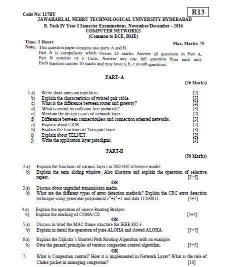
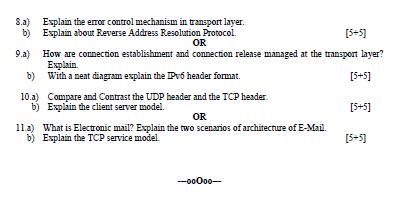
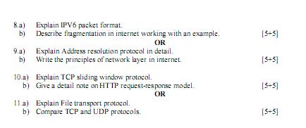
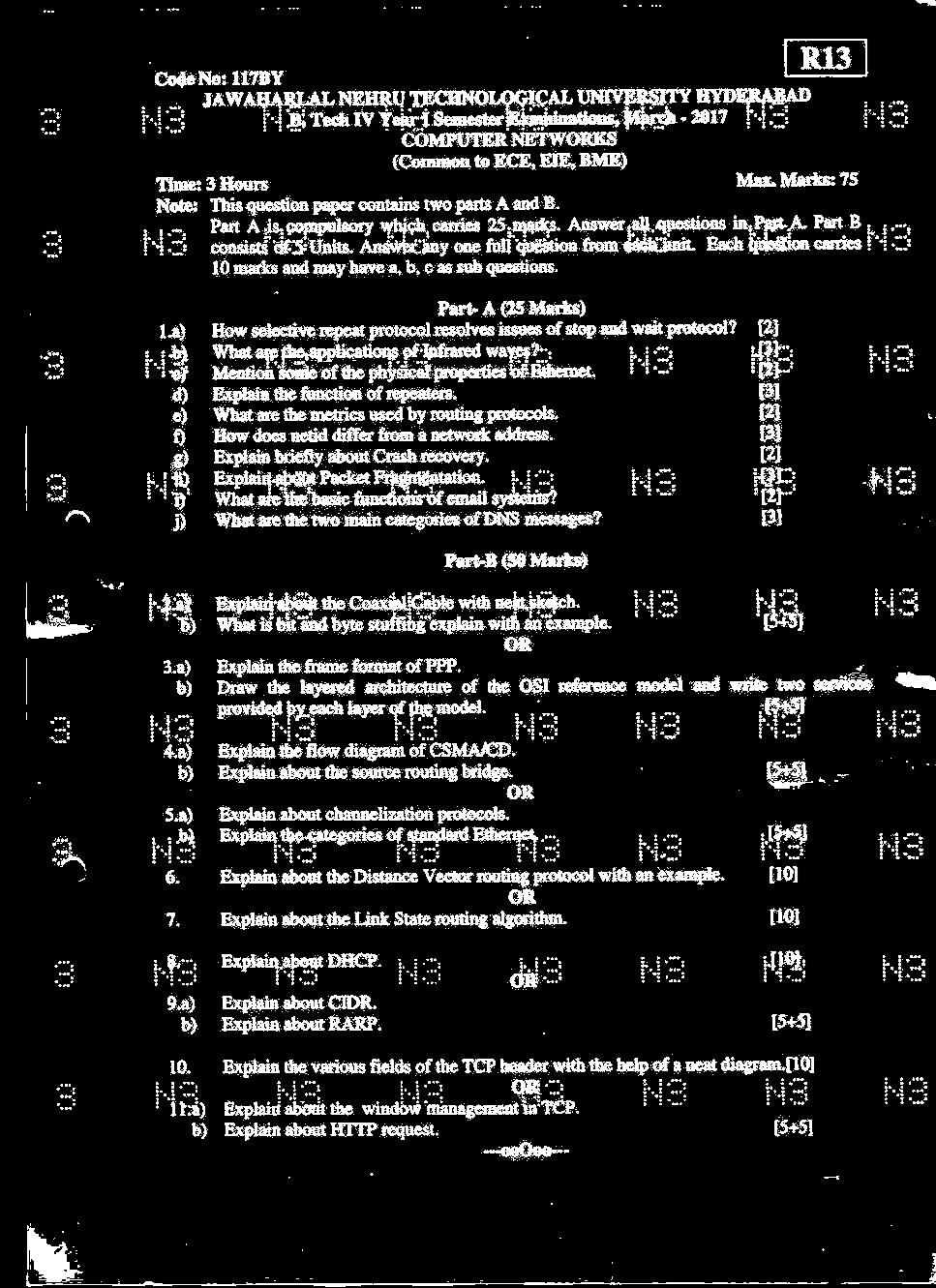
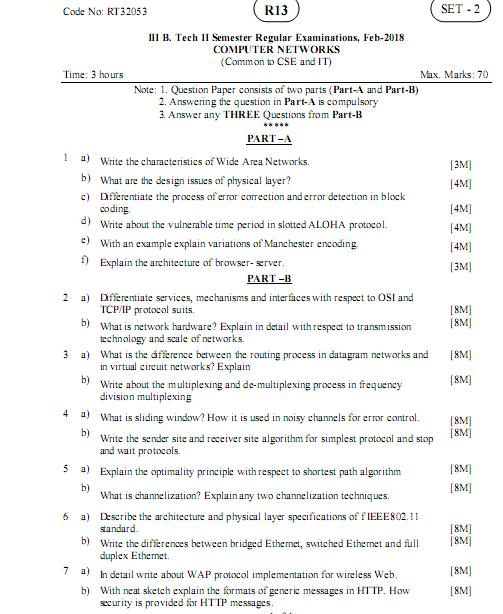
41 Code No: R15A0514 MALLA REDDY COLLEGE OF ENGINEERING &TECHNOLOGY (Autonomous Institution UGC, Govt. of India) B. Tech IV Year I Semester Examinations Computer Networks (Electronics Communication and Engineering) Time: 3hours Max Marks: 70 Note: This question paper contains two questions from each of five Units. Answer any one full question from each unit. Each question carries 14 marks and may have a, b, c as sub questions. 1. Explain ISO OSI Reference model with neat sketch. (14M) 2. Explain different kinds of Transmission Media. (14M) 3. Explain CSMA and CSMA/CD in detail. (14M) 4. a) What do you mean by bit stuffing and why it is employed. (7M) b) Explain error detection using Checksum. (7M) 5. a) Compare and contrast TDM, STDM and FDM. (14M) b) What are the common Fast Ethernet implementations? Give the purpose of NIC (7M) 6. a) Explain indetail about different Bluetooth layers. (7M) b) wwhat are the advantages of dividing an Ethernet LAN with a bridge? Give the relationship between a switch and a bridge (7M) 7. a) With the aid of necessary explain in detail about significance of tunneling. (7M) b) Explain DHCP. (7M) 8. a) Write short notes on Link state routing. (7M) b) Explain the process of physical address to logical address mapping using Boot Strap Protocol. (7M) 9. a) Explain UDP header format. (7M) b) Write short notes on congestion control. (7M) 10. Explain the following a) FTP (7M) b) DNS (7M)
42 Code No: R15A0514 MALLA REDDY COLLEGE OF ENGINEERING &TECHNOLOGY (Autonomous Institution UGC, Govt. of India) B. Tech IV Year I Semester Examinations Computer Networks (Electronics Communication and Engineering) Time: 3hours Max Marks: 70 Note: This question paper contains two questions from each of five Units. Answer any one full question from each unit. Each question carries 14 marks and may have a, b, c as sub questions. 1. Explain TCP/IP Protocol Suit with neat sketch and list out differences between TCP/IP and OSI model (14M) 2. Write short notes on internet. (14M) 3. a) Explain about services provided by PPP and also list out the services that are not provided by PPP. (7M) b) Explain Pure and derive expression for its throughput. (7M) 4. a) Explain about different strategies that are employed under controlled access. (6M) b) Explain in detail about working of TDMA and also list out differences between TDMA, FDMA and CDMA. (8M) 5. a) Write short notes on giga bit ethernet. (14M) b) Explain in detail about hidden and exposed node problems in wireless lans 6. What do you mean by virtual lan and explain in detail about configuring and maintaing data of virtual lans. (7M) With the aid of suitable example explain about frequency reuse principle. (7M) 7. a) Explain in detail about IGMP. (7M) b) Is multicast routing is same as multiple unicast routing, Explain. And also write short notes on MOSPF (7M) 8. a) Explain Transport layer Connection Establishment and Connection Release. (7M) b) Explain Transport protocol addressing. (7M)
43 9. a) Explain TCP header format. (7M) b) Explain TCP Congestion Control. (7M) 10. Explain the following a) SMTP (7M) b) HTTP (7M)
44 Code No: R15A0514 MALLA REDDY COLLEGE OF ENGINEERING &TECHNOLOGY (Autonomous Institution UGC, Govt. of India) B. Tech IV Year I Semester Examinations Computer Networks (Electronics Communication and Engineering) Time: 3hours Max Marks: 70 Note: This question paper contains two questions from each of five Units. Answer any one full question from each unit. Each question carries 14 marks and may have a, b, c as sub questions. 1. a) Explain in detail about layering scenario. (6M) b) Write short notes on different levels of addressing mechanism employed in internet (8M) 2. Explain different kinds transmission media used for internet. (14M) 3. a) Explain error detection using CRC for the following. Consider a message represented by the polynomial M(x) = x5 + x4 + x and a generating polynomial G(x) = x3 + x2 + 1 (1101) (7M) b) Explain in detail about different fields present in PPP frame format. (7M) 4. a) Draw and explain HDLC frame format and also explain about different types of frames used in HDLC. (8M) b) Explain how slotted aloha improves the performance of pure aloha (7M) 5. a) Discuss briefly about the MAC layers in the standard. (14M) b) Explain in detail about the Physical layer in the Fast Ethernet 6. a) Describe in detail about the Frequency Division Multiple Access. (14M) b) What is learning bridge and explain in detail about the process of learning of learning bridge (7M) 7. a) Write short notes on IPV6 addresses. (7M) b) Explain indetail about message format and different types of error reporting messages of ICMP. (7M) 8. With a suitable example explain Distance Vector Routing algorithm. What is the serious drawback of Distance Vector Routing algorithm? Explain. (14M)
45 9. a) Explain TCP header format. (7M) b) What is WEB Documents? Explain with its categories. (7M) 10. a)write short notes on SMTP (7M) b) Write short notes of different techniques that are employed to improve QoS (7M)
46 Code No: R15A0514 MALLA REDDY COLLEGE OF ENGINEERING &TECHNOLOGY (Autonomous Institution UGC, Govt. of India) B. Tech IV Year I Semester Examinations Computer Networks (Electronics Communication and Engineering) Time: 3hours Max Marks: 70 Note: This question paper contains two questions from each of five Units. Answer any one full question from each unit. Each question carries 14 marks and may have a, b, c as sub questions. 1. a) Explain in detail about layering scenario. (6M) b) Write short notes on different levels of addressing mechanism employed in internet (8M) 2. Explain different kinds transmission media used for internet. (14M) 3. a)given data frame and generator polynomial G(x) = x4 + x + 1. Derive the transmitted frame (7M) b) Explain in detail about CSMA/CA. (7M) 4. a) Explain in detail about CSMS/CD (8M) b) Give a brief note on the Multilink Point to point protocol (7M) 5. a) Why there is no need for CSMA/CD on a full-duplex Ethernet LAN? Explain. (14M) b) Write short on back bone networks 6. a) Describe in detail about the CDMA. (7M) b) Write short notes on IEEE (7M) 7. a) Explain briefly about the shortest path routing algorithm. (6M) b) Explain indetail about classfull addressing and classless addressing. (8M) 8. a) What is Count to infinity problem? Explain with suitable example. (7M) b) Write short notes on internetworking (7M)
47 9. a) Draw frame format of SCTP and discuss indetail about each field. Also list out differences between SCTP and TCP. (7M) b) Write short notes of different techniques that are employed to improve QoS (7M) 10. a) List out the different fields that are missing in TCP header as compared to that of UDP and give the reasons for their missing. (7M) b) What is WEB Documents? Explain with its categories. (7M)
48 PREVIOUS QUESTION PAPERS FROM OTHER UNIVERSITIES (JNTUH-2016 & 2017)
49
50
51
52
53

54
55 PREVIOUS QUESTION PAPERS FROM OTHER UNIVERSITIES (JNTUK-2018)

56
57
58
59
INSTITUTE OF AERONAUTICAL ENGINEERING (Autonomous) Dundigal, Hyderabad
 Dundigal, Hyderabad") INSTITUTE OF AERONAUTICAL ENGINEERING (Autonomous) Dundigal, Hyderabad - 500 043 ELECTRONICS AND COMMUNICATION ENGINEERING TUTORIAL BANK Name : MICROWAVE ENGINEERING Code : A70442 Class : IV B. Tech I
INSTITUTE OF AERONAUTICAL ENGINEERING (Autonomous) Dundigal, Hyderabad - 500 043 ELECTRONICS AND COMMUNICATION ENGINEERING TUTORIAL BANK Name : MICROWAVE ENGINEERING Code : A70442 Class : IV B. Tech I
EC 1402 Microwave Engineering
 SHRI ANGALAMMAN COLLEGE OF ENGINEERING & TECHNOLOGY (An ISO 9001:2008 Certified Institution) SIRUGANOOR,TRICHY-621105. DEPARTMENT OF ELECTRONICS AND COMMUNICATION ENGINEERING EC 1402 Microwave Engineering
St.MARTIN S ENGINEERING COLLEGE Dhulapally, Secunderabad
 St.MARTIN S ENGINEERING COLLEGE Dhulapally, Secunderabad 500014. Department of Electronics and Communication Engineering SUB: MICROWAVE ENGINEERING SECTION: ECE IV A & B NAME OF THE FACULTY: S RAVI KUMAR,T.SUDHEER
3. (a) Derive an expression for the Hull cut off condition for cylindrical magnetron oscillator. (b) Write short notes on 8 cavity magnetron [8+8]
![3. (a) Derive an expression for the Hull cut off condition for cylindrical magnetron oscillator. (b) Write short notes on 8 cavity magnetron [8+8]](/thumbs/73/68588725.jpg "3. (a) Derive an expression for the Hull cut off condition for cylindrical magnetron oscillator. (b) Write short notes on 8 cavity magnetron [8+8]") Code No: RR320404 Set No. 1 1. (a) Compare Drift space bunching and Reflector bunching with the help of Applegate diagrams. (b) A reflex Klystron operates at the peak of n=1 or 3 / 4 mode. The dc power
Code No: RR320404 Set No. 1 1. (a) Compare Drift space bunching and Reflector bunching with the help of Applegate diagrams. (b) A reflex Klystron operates at the peak of n=1 or 3 / 4 mode. The dc power
DEPARTMENT OF ELECTRONICS AND COMMUNICATION ENGINEERING QUESTION BANK SUBJECT NAME & CODE: EC2403 & RF AND MICROWAVE ENGINEERING UNIT I
 FATIMA MICHAEL COLLEGE OF ENGINEERING & TECHNOLOGY Senkottai Village, Madurai Sivagangai Main Road, Madurai -625 020 An ISO 9001:2008 Certified Institution DEPARTMENT OF ELECTRONICS AND COMMUNICATION ENGINEERING
R.K.YADAV. 2. Explain with suitable sketch the operation of two-cavity Klystron amplifier. explain the concept of velocity and current modulations.
 Question Bank DEPARTMENT OF ELECTRONICS AND COMMUNICATION SUBJECT- MICROWAVE ENGINEERING(EEC-603) Unit-III 1. What are the high frequency limitations of conventional tubes? Explain clearly. 2. Explain
QUESTION BANK SUB. NAME: RF & MICROWAVE ENGINEERING SUB. CODE: EC 2403 BRANCH/YEAR/: ECE/IV UNIT 1 TWO PORT RF NETWORKS- CIRCUIT REPRESENTATION
 QUESTION BANK SUB. NAME: RF & MICROWAVE ENGINEERING SUB. CODE: EC 2403 SEM: VII BRANCH/YEAR/: ECE/IV UNIT 1 TWO PORT RF NETWORKS- CIRCUIT REPRESENTATION 1. What is RF? 2. What is an RF tuner? 3. Define
. From the above data, determine the network is symmetric or not.
 Velammal College of Engineering and Technology, Madurai Department of Electronics and Communication Engineering Question Bank Subject Name: EC2353 Antennas And Wave Propagation Faculty: Mrs G VShirley
EC 1354-Principles of VLSI Design
 EC 1354-Principles of VLSI Design UNIT I MOS TRANSISTOR THEORY AND PROCESS TECHNOLOGY PART-A 1. What are the four generations of integrated circuits? 2. Give the advantages of IC. 3. Give the variety of
MICROWAVE ENGINEERING-II. Unit- I MICROWAVE MEASUREMENTS
 MICROWAVE ENGINEERING-II Unit- I MICROWAVE MEASUREMENTS 1. Explain microwave power measurement. 2. Why we can not use ordinary diode and transistor in microwave detection and microwave amplification? 3.
Time: 3 hours Max Marks: 70 Answer any FIVE questions All questions carry equal marks *****
 Code: 9A04601 DIGITAL COMMUNICATIONS (Electronics and Communication Engineering) 1 (a) Explain in detail about non-uniform quantization. (b) What is the disadvantage of uniform quantization over the non-uniform
MICROWAVE ENGINEERING LAB VIVA QUESTIONS AND ANSWERS
 MICROWAVE ENGINEERING LAB VIVA QUESTIONS AND ANSWERS. Why can t conventional tubes be used at microwave frequencies? Conventional tubes can t be used at microwave frequencies because of transit time effect.
GUJARAT TECHNOLOGICAL UNIVERSITY, AHMEDABAD, GUJARAT COURSE CURRICULUM COURSE TITLE: MICROWAVE & RADAR ENGINEERING (COURSE CODE: )
") GUJARAT TECHNOLOGICAL UNIVERSITY, AHMEDABAD, GUJARAT COURSE CURRICULUM COURSE TITLE: MICROWAVE & RADAR ENGINEERING (COURSE CODE: 3351103) Diploma Programme in which this course is offered Electronics and
GUJARAT TECHNOLOGICAL UNIVERSITY, AHMEDABAD, GUJARAT COURSE CURRICULUM COURSE TITLE: MICROWAVE & RADAR ENGINEERING (COURSE CODE: 3351103) Diploma Programme in which this course is offered Electronics and
Microwave Devices and Circuit Design
 Microwave Devices and Circuit Design Ganesh Prasad Srivastava Vijay Laxmi Gupta MICROWAVE DEVICES and CIRCUIT DESIGN GANESH PRASAD SRIVASTAVA Professor (Retired) Department of Electronic Science University
TECHNO INDIA BATANAGAR (DEPARTMENT OF ELECTRONICS & COMMUNICATION ENGINEERING) QUESTION BANK- 2018
 QUESTION BANK- 2018") TECHNO INDIA BATANAGAR (DEPARTMENT OF ELECTRONICS & COMMUNICATION ENGINEERING) QUESTION BANK- 2018 Paper Setter Detail Name Designation Mobile No. E-mail ID Raina Modak Assistant Professor 6290025725 raina.modak@tib.edu.in
TECHNO INDIA BATANAGAR (DEPARTMENT OF ELECTRONICS & COMMUNICATION ENGINEERING) QUESTION BANK- 2018 Paper Setter Detail Name Designation Mobile No. E-mail ID Raina Modak Assistant Professor 6290025725 raina.modak@tib.edu.in
(8+8) 6. (a) Explain the following in detail concern to the mobile system?
 6. (a) Explain the following in detail concern to the mobile system?") SET - 1 1. (a) Explain the operation of the cellular system? (b) Discuss analog cellular systems (AMPS) in detail? 2. (a) What is meant by frequency reuse? Explain various frequency reuse schemes and find
SET - 1 1. (a) Explain the operation of the cellular system? (b) Discuss analog cellular systems (AMPS) in detail? 2. (a) What is meant by frequency reuse? Explain various frequency reuse schemes and find
INSTITUTE OF AERONAUTICAL ENGINEERING (Autonomous) Dundigal, Hyderabad
 Dundigal, Hyderabad") INSTITUTE OF AERONAUTICAL ENGINEERING (Autonomous) Dundigal, Hyderabad - 500 0 ELECTRONICS AND COMMUNICATION ENGINEERING TUTORIAL QUESTION BANK Name : VLSI Design Code : A0 Regulation : R5 Structure :
INSTITUTE OF AERONAUTICAL ENGINEERING (Autonomous) Dundigal, Hyderabad - 500 0 ELECTRONICS AND COMMUNICATION ENGINEERING TUTORIAL QUESTION BANK Name : VLSI Design Code : A0 Regulation : R5 Structure :
SHORT QUESTIONS MICROWAVE ENGINEERING UNIT I
 SHORT QUESTIONS MICROWAVE ENGINEERING UNIT I 1. Define Microwave. Microwaves are generally described as electromagnetic waves with frequencies that range from approximately 1GHz to 300 GHz. Therefore,
MICROWAVE AND RADAR LAB (EE-322-F) LAB MANUAL VI SEMESTER
 LAB MANUAL VI SEMESTER") 1 MICROWAVE AND RADAR LAB (EE-322-F) MICROWAVE AND RADAR LAB (EE-322-F) LAB MANUAL VI SEMESTER RAO PAHALD SINGH GROUP OF INSTITUTIONS BALANA(MOHINDERGARH)123029 Department Of Electronics and Communication
1 MICROWAVE AND RADAR LAB (EE-322-F) MICROWAVE AND RADAR LAB (EE-322-F) LAB MANUAL VI SEMESTER RAO PAHALD SINGH GROUP OF INSTITUTIONS BALANA(MOHINDERGARH)123029 Department Of Electronics and Communication
LESSON PLAN. LESSON PLAN DURATION : - 15 weeks (from JULY 2018 to NOVEMBER 2018)
") LESSON PLAN NAME OF THE FACULTY DISCIPLINE SEMESTER SUBJECT : - HIMANSHU YADAV : - ECE : - FIFTH : - MICROWAVE ENGG LESSON PLAN DURATION : - 15 weeks (from JULY 2018 to NOVEMBER 2018) WORK LOAD (LECTURE/PRACTICAL)
LESSON PLAN NAME OF THE FACULTY DISCIPLINE SEMESTER SUBJECT : - HIMANSHU YADAV : - ECE : - FIFTH : - MICROWAVE ENGG LESSON PLAN DURATION : - 15 weeks (from JULY 2018 to NOVEMBER 2018) WORK LOAD (LECTURE/PRACTICAL)
 VALLIAMMAI ENGINEERING COLLEGE SRM Nagar, Kattankulathur-603 203 DEPARTMENT OF ELECTRONICS AND COMMUNICATION ENGINEERING EC6503 TRANSMISSION LINES AND WAVEGUIDES YEAR / SEMESTER: III / V ACADEMIC YEAR:
Master of Comm. Systems Engineering (Structure C)
") ENGINEERING Master of Comm. DURATION 1.5 YEARS 3 YEARS (Full time) 2.5 YEARS 4 YEARS (Part time) P R O G R A M I N F O Master of Communication System Engineering is a quarter research program where candidates
ENGINEERING Master of Comm. DURATION 1.5 YEARS 3 YEARS (Full time) 2.5 YEARS 4 YEARS (Part time) P R O G R A M I N F O Master of Communication System Engineering is a quarter research program where candidates
PRINCIPLES OF RADAR. By Members of the Staff of the Radar School Massachusetts Institute of Technology. Third Edition by J.
 PRINCIPLES OF RADAR By Members of the Staff of the Radar School Massachusetts Institute of Technology Third Edition by J. Francis Reintjes ASSISTANT PBOFESSOR OF COMMUNICATIONS MASSACHUSETTS INSTITUTE
QUESTION BANK FOR IV B.TECH II SEMESTER ( )
") DEPARTMENT OF ELECTRONICS & COMMUNICATION ENGINEERING QUESTION BANK F IV B.TECH II SEMESTER (2018 19) MALLA REDDY COLLEGE OF ENGINEERING &TECHNOLOGY (Autonomous Institution UGC, Govt. of India) (Affiliated
DEPARTMENT OF ELECTRONICS & COMMUNICATION ENGINEERING QUESTION BANK F IV B.TECH II SEMESTER (2018 19) MALLA REDDY COLLEGE OF ENGINEERING &TECHNOLOGY (Autonomous Institution UGC, Govt. of India) (Affiliated
R.B.V.R.R. WOMEN S COLLEGE (AUTONOMOUS) Narayanaguda, Hyderabad. ELECTRONIC PRINCIPLES AND APPLICATIONS
 Narayanaguda, Hyderabad. ELECTRONIC PRINCIPLES AND APPLICATIONS") R.B.V.R.R. WOMEN S COLLEGE (AUTONOMOUS) Narayanaguda, Hyderabad. DEPARTMENT OF PHYSICS QUESTION BANK FOR SEMESTER V PHYSICS PAPER VI (A) ELECTRONIC PRINCIPLES AND APPLICATIONS UNIT I: SEMICONDUCTOR DEVICES
R.B.V.R.R. WOMEN S COLLEGE (AUTONOMOUS) Narayanaguda, Hyderabad. DEPARTMENT OF PHYSICS QUESTION BANK FOR SEMESTER V PHYSICS PAPER VI (A) ELECTRONIC PRINCIPLES AND APPLICATIONS UNIT I: SEMICONDUCTOR DEVICES
MAHAVEER INSTITUTE OF SCIENCE & TECHNOLOGY. Microwave and Digital Communications Lab. Department Of Electronics and Communication Engineering
 MAHAVEER INSTITUTE OF SCIENCE & TECHNOLOGY Microwave and Digital Communications Lab Department Of Electronics and Communication Engineering MICROWAVE ENGINEERING LAB List of Experiments: 1.Reflex Klystron
SRM INSTITUTE OF SCIENCE AND TECHNOLOGY (DEEMED UNIVERSITY)
") SRM INSTITUTE OF SCIENCE AND TECHNOLOGY (DEEMED UNIVERSITY) QUESTION BANK I YEAR B.Tech (II Semester) ELECTRONIC DEVICES (COMMON FOR EC102, EE104, IC108, BM106) UNIT-I PART-A 1. What are intrinsic and
SRM INSTITUTE OF SCIENCE AND TECHNOLOGY (DEEMED UNIVERSITY) QUESTION BANK I YEAR B.Tech (II Semester) ELECTRONIC DEVICES (COMMON FOR EC102, EE104, IC108, BM106) UNIT-I PART-A 1. What are intrinsic and
(i) Determine the admittance parameters of the network of Fig 1 (f) and draw its - equivalent circuit.
 Determine the admittance parameters of the network of Fig 1 (f) and draw its - equivalent circuit.") I.E.S-(Conv.)-1995 ELECTRONICS AND TELECOMMUNICATION ENGINEERING PAPER - I Some useful data: Electron charge: 1.6 10 19 Coulomb Free space permeability: 4 10 7 H/m Free space permittivity: 8.85 pf/m Velocity
I.E.S-(Conv.)-1995 ELECTRONICS AND TELECOMMUNICATION ENGINEERING PAPER - I Some useful data: Electron charge: 1.6 10 19 Coulomb Free space permeability: 4 10 7 H/m Free space permittivity: 8.85 pf/m Velocity
Academic Course Description. EC1022 Microwave and Optical Communications Sixth Semester, (even semester)
") Academic Course Description EC1022 Microwave and Optical Communications SRM University Faculty of Engineering and Technology Department of Electronics and Communication Engineering EC1022 Microwave and
Academic Course Description EC1022 Microwave and Optical Communications SRM University Faculty of Engineering and Technology Department of Electronics and Communication Engineering EC1022 Microwave and
MICROWAVE ENGINEERING LECTURE NOTES B.TECH (IV YEAR I SEM) ( )
 ( )") MICROWAVE ENGINEERING LECTURE NOTES B.TECH (IV YEAR I SEM) (2018-19) Prepared by: M SREEDHAR REDDY, Asst.Prof. ECE RENJU PANICKER, Asst.Prof. ECE Department of Electronics and Communication Engineering
MICROWAVE ENGINEERING LECTURE NOTES B.TECH (IV YEAR I SEM) (2018-19) Prepared by: M SREEDHAR REDDY, Asst.Prof. ECE RENJU PANICKER, Asst.Prof. ECE Department of Electronics and Communication Engineering
CMOS Digital Logic Design with Verilog. Chapter1 Digital IC Design &Technology
 CMOS Digital Logic Design with Verilog Chapter1 Digital IC Design &Technology Chapter Overview: In this chapter we study the concept of digital hardware design & technology. This chapter deals the standard
MICROWAVE MICROWAVE TRAINING BENCH COMPONENT SPECIFICATIONS:
 Microwave section consists of Basic Microwave Training Bench, Advance Microwave Training Bench and Microwave Communication Training System. Microwave Training System is used to study all the concepts of
For the mechanical system of figure shown above:
 I.E.S-(Conv.)-00 ELECTRONICS AND TELECOMMUNICATION ENGINEERING PAPER - I Time Allowed: Three Hours Maximum Marks : 0 Candidates should attempt any FIVE questions. Some useful data: Electron charge : 1.6
Syllabus for Entrance Test for Ph.D. Admissions Department of ECE, ETE, E&I
 Syllabus for Entrance Test for Ph.D. Admissions Department of ECE, ETE, E&I ELECTRONICS AND COMMUNICATION SYSTEMS Baseband Data Transmission: Signal and Systems, probability and Random variables, Digital
Microwave Fundamentals A Survey of Microwave Systems and Devices p. 3 The Relationship of Microwaves to Other Electronic Equipment p.
 Microwave Fundamentals A Survey of Microwave Systems and Devices p. 3 The Relationship of Microwaves to Other Electronic Equipment p. 3 Microwave Systems p. 5 The Microwave Spectrum p. 6 Why Microwave
Lesson Plan. WEEK Theory Practical Lecture Day Topic(including assignment/test) Practical Day Topic
 Practical Day Topic") Lesson Plan Name of the Faculty : Mr. Sandeep Kumar (Theory) Discipline : B.TECH (ECE ) Semester : 6 th semester Subject : VLSI Design Lesson plan Duration : 15 Weeks (from January, 2018 to April, 2018)
Lesson Plan Name of the Faculty : Mr. Sandeep Kumar (Theory) Discipline : B.TECH (ECE ) Semester : 6 th semester Subject : VLSI Design Lesson plan Duration : 15 Weeks (from January, 2018 to April, 2018)
Lecture 12 Memory Circuits. Memory Architecture: Decoders. Semiconductor Memory Classification. Array-Structured Memory Architecture RWM NVRWM ROM
 Semiconductor Memory Classification Lecture 12 Memory Circuits RWM NVRWM ROM Peter Cheung Department of Electrical & Electronic Engineering Imperial College London Reading: Weste Ch 8.3.1-8.3.2, Rabaey
SRM UNIVERSITY FACULTY OF ENGINEERING AND TECHNOLOGY SCHOOL OF ELECTRONICS AND ELECTRICAL ENGINEERING DEPARTMENT OF TCE COURSE PLAN
 SRM UNIVERSITY FACULTY OF ENGINEERING AND TECHNOLOGY SCHOOL OF ELECTRONICS AND ELECTRICAL ENGINEERING DEPARTMENT OF TCE COURSE PLAN Course Code : TE1018 Course Title : Microwave Radio And Optical Fiber
PHYSICAL STRUCTURE OF CMOS INTEGRATED CIRCUITS. Dr. Mohammed M. Farag
 PHYSICAL STRUCTURE OF CMOS INTEGRATED CIRCUITS Dr. Mohammed M. Farag Outline Integrated Circuit Layers MOSFETs CMOS Layers Designing FET Arrays EE 432 VLSI Modeling and Design 2 Integrated Circuit Layers
A Survey of the Low Power Design Techniques at the Circuit Level
 A Survey of the Low Power Design Techniques at the Circuit Level Hari Krishna B Assistant Professor, Department of Electronics and Communication Engineering, Vagdevi Engineering College, Warangal, India
Module-3: Metal Oxide Semiconductor (MOS) & Emitter coupled logic (ECL) families
 & Emitter coupled logic (ECL) families") 1 Module-3: Metal Oxide Semiconductor (MOS) & Emitter coupled logic (ECL) families 1. Introduction 2. Metal Oxide Semiconductor (MOS) logic 2.1. Enhancement and depletion mode 2.2. NMOS and PMOS inverter
1 Module-3: Metal Oxide Semiconductor (MOS) & Emitter coupled logic (ECL) families 1. Introduction 2. Metal Oxide Semiconductor (MOS) logic 2.1. Enhancement and depletion mode 2.2. NMOS and PMOS inverter
Hours / 100 Marks Seat No.
 17656 16117 3 Hours / 100 Seat No. Instructions (1) All Questions are Compulsory. (2) Answer each next main Question on a new page. (3) Assume suitable data, if necessary. (4) Use of Non-programmable Electronic
EC Transmission Lines And Waveguides
 EC6503 - Transmission Lines And Waveguides UNIT I - TRANSMISSION LINE THEORY A line of cascaded T sections & Transmission lines - General Solution, Physical Significance of the Equations 1. Define Characteristic
RAJIV GANDHI COLLEGE OF ENGINEERING AND TECHNOLOGY Kirumampakkam,Puducherry DEPARTMENT OF ELECTRONICS AND COMMUNICATION ENGINEERING
 RAJIV GANDHI COLLEGE OF ENGINEERING AND TECHNOLOGY Kirumampakkam,Puducherry-607402 DEPARTMENT OF ELECTRONICS AND COMMUNICATION ENGINEERING QUESTION BANK FOR EC T55 - TRANSMISSION LINES AND WAVEGUIDES G.LAXMINARAYANAN,
LINEAR IC APPLICATIONS
 1 B.Tech III Year I Semester (R09) Regular & Supplementary Examinations December/January 2013/14 1 (a) Why is R e in an emitter-coupled differential amplifier replaced by a constant current source? (b)
 I.E.S-(Conv.)-2007 ELECTRONICS AND TELECOMMUNICATION ENGINEERING PAPER - II Time Allowed: 3 hours Maximum Marks : 200 Candidates should attempt Question No. 1 which is compulsory and FOUR more questions
PESIT BANGALORE SOUTH CAMPUS BASIC ELECTRONICS
 PESIT BANGALORE SOUTH CAMPUS QUESTION BANK BASIC ELECTRONICS Sub Code: 17ELN15 / 17ELN25 IA Marks: 20 Hrs/ Week: 04 Exam Marks: 80 Total Hours: 50 Exam Hours: 03 Name of Faculty: Mr. Udoshi Basavaraj Module
Academic Course Description
 BEC010- VLSI Design Academic Course Description BHARATH UNIVERSITY Faculty of Engineering and Technology Department of Electronics and Communication Engineering BEC010 VLSI Design Sixth Semester (Elective)
EC6503 Transmission Lines and WaveguidesV Semester Question Bank
 UNIT I TRANSMISSION LINE THEORY A line of cascaded T sections & Transmission lines General Solution, Physicasignificance of the equations 1. Derive the two useful forms of equations for voltage and current
CHAPTER 4. Practical Design
 CHAPTER 4 Practical Design The results in Chapter 3 indicate that the 2-D CCS TL can be used to synthesize a wider range of characteristic impedance, flatten propagation characteristics, and place passive
Academic Course Description
 BEC010- VLSI Design Academic Course Description BHARATH UNIVERSITY Faculty of Engineering and Technology Department of Electronics and Communication Engineering BEC010 VLSI Design Fifth Semester (Elective)
UNIT-III. 1. Define cochannel interference. How is it measured at the mobile unit and cell site?
 UNIT-III 1. Define cochannel interference. How is it measured at the mobile unit and cell site? Answer: Cochannel Interference: The frequency-re method is useful for increasing the efficiency of spectrum
problem grade total
 Fall 2005 6.012 Microelectronic Devices and Circuits Prof. J. A. del Alamo Name: Recitation: November 16, 2005 Quiz #2 problem grade 1 2 3 4 total General guidelines (please read carefully before starting):
DAV Institute of Engineering & Technology Department of ECE. Course Outcomes
 DAV Institute of Engineering & Technology Department of ECE Course Outcomes Upon successful completion of this course, the student will intend to apply the various outcome as:: BTEC-301, Analog Devices
RF AND MICROWAVE ENGINEERING
 RF AND MICROWAVE ENGINEERING FUNDAMENTALS OF WIRELESS COMMUNICATIONS Frank Gustrau Dortmund University of Applied Sciences and Arts, Germany WILEY A John Wiley & Sons, Ltd., Publication Preface List of
ECE 5745 Complex Digital ASIC Design Topic 2: CMOS Devices
 ECE 5745 Complex Digital ASIC Design Topic 2: CMOS Devices Christopher Batten School of Electrical and Computer Engineering Cornell University http://www.csl.cornell.edu/courses/ece5950 Simple Transistor
Downloaded From All JNTU World
 Code: 9A02401 PRINCIPLES OF ELECTRICAL ENGINEERING (Common to ECE, EIE, E.Con.E & ECC) 1 Find initial conditions for voltage across capacitor, the currents i 1, i 2 and the derivatives for the circuit
Transistor was first invented by William.B.Shockley, Walter Brattain and John Bardeen of Bell Labratories. In 1961, first IC was introduced.
 Unit 1 Basic MOS Technology Transistor was first invented by William.B.Shockley, Walter Brattain and John Bardeen of Bell Labratories. In 1961, first IC was introduced. Levels of Integration:- i) SSI:-
Hot Topics and Cool Ideas in Scaled CMOS Analog Design
 Engineering Insights 2006 Hot Topics and Cool Ideas in Scaled CMOS Analog Design C. Patrick Yue ECE, UCSB October 27, 2006 Slide 1 Our Research Focus High-speed analog and RF circuits Device modeling,
ECE/CoE 0132: FETs and Gates
 ECE/CoE 0132: FETs and Gates Kartik Mohanram September 6, 2017 1 Physical properties of gates Over the next 2 lectures, we will discuss some of the physical characteristics of integrated circuits. We will
Designing a 960 MHz CMOS LNA and Mixer using ADS. EE 5390 RFIC Design Michelle Montoya Alfredo Perez. April 15, 2004
 Designing a 960 MHz CMOS LNA and Mixer using ADS EE 5390 RFIC Design Michelle Montoya Alfredo Perez April 15, 2004 The University of Texas at El Paso Dr Tim S. Yao ABSTRACT Two circuits satisfying the
Course Outcome of M.Tech (VLSI Design)
") Course Outcome of M.Tech (VLSI Design) PVL108: Device Physics and Technology The students are able to: 1. Understand the basic physics of semiconductor devices and the basics theory of PN junction. 2.
Course Outcome of M.Tech (VLSI Design) PVL108: Device Physics and Technology The students are able to: 1. Understand the basic physics of semiconductor devices and the basics theory of PN junction. 2.
(DEC 411) B.Tech. DEGREE EXAMINATION, MAY (Examination at the end of Final Year) Electronics and Communication Engineering INDUSTRIAL MANAGEMENT
 B.Tech. DEGREE EXAMINATION, MAY (Examination at the end of Final Year) Electronics and Communication Engineering INDUSTRIAL MANAGEMENT") (DEC 411) B.Tech. DEGREE EXAMINATION, MAY 2011. (Examination at the end of Final Year) Electronics and Communication Engineering Time : Three hours INDUSTRIAL MANAGEMENT Maximum : 75 marks Question No.
(DEC 411) B.Tech. DEGREE EXAMINATION, MAY 2011. (Examination at the end of Final Year) Electronics and Communication Engineering Time : Three hours INDUSTRIAL MANAGEMENT Maximum : 75 marks Question No.
Preface to Third Edition Deep Submicron Digital IC Design p. 1 Introduction p. 1 Brief History of IC Industry p. 3 Review of Digital Logic Gate
 Preface to Third Edition p. xiii Deep Submicron Digital IC Design p. 1 Introduction p. 1 Brief History of IC Industry p. 3 Review of Digital Logic Gate Design p. 6 Basic Logic Functions p. 6 Implementation
Design of Duplexers for Microwave Communication Systems Using Open-loop Square Microstrip Resonators
 International Journal of Electromagnetics and Applications 2016, 6(1): 7-12 DOI: 10.5923/j.ijea.20160601.02 Design of Duplexers for Microwave Communication Charles U. Ndujiuba 1,*, Samuel N. John 1, Taofeek
Microwave Technology
 GUC (Dr. Hany Hammad) 9/5/06 Microwave Technology (COMM 903) Contents Introduction: Course contents. Assessment. eferences. Microwave Sources. Transistor Model Extraction. Signal flow graphs. COMM (903)
VL0306-VLSI Devices & Design. L T P C EC0306 VLSI DEVICES AND DESIGN Prerequisite : EC0205 & EC0203 Course outcomes
 Page 1 VL0306-VLSI Devices & Design L T P C EC0306 VLSI DEVICES AND DESIGN 2 2 0 3 Prerequisite : EC0205 & EC0203 Course outcomes the ability to identify, formulate and solve engineering problems i) Graduate
 I.E.S-(Conv.)-2005 ELECTRONICS AND TELECOMMUNICATION ENGINEERING PAPER - II Time Allowed: 3 hours Maximum Marks : 200 Candidates should attempt Question No. 1 which is compulsory and FOUR more questions
EC TRANSMISSION LINES AND WAVEGUIDES TRANSMISSION LINES AND WAVEGUIDES
 TRANSMISSION LINES AND WAVEGUIDES UNIT I - TRANSMISSION LINE THEORY 1. Define Characteristic Impedance [M/J 2006, N/D 2006] Characteristic impedance is defined as the impedance of a transmission line measured
CHAPTER - 6 PIN DIODE CONTROL CIRCUITS FOR WIRELESS COMMUNICATIONS SYSTEMS
 CHAPTER - 6 PIN DIODE CONTROL CIRCUITS FOR WIRELESS COMMUNICATIONS SYSTEMS 2 NOTES 3 INTRODUCTION PIN DIODE CONTROL CIRCUITS FOR WIRELESS COMMUNICATIONS SYSTEMS Chapter 6 discusses PIN Control Circuits
Semester-VI. Course Code Course Title L P Credit. ECE 601T Microwave Engineering 4 0 4
 Semester-VI Course Code Course Title L P Credit ECE 601T Microwave Engineering 4 0 4 ECE 602T Antennas, Wave Propagation and Transmission Lines 4 0 4 ECE 603T Linear Integrated Circuits 4 0 4 ECE 604T
VALLIAMMAI ENGINEERING COLLEGE
 VALLIAMMAI ENGINEERING COLLEGE SRM Nagar, Kattankulathur 603 203 DEPARTMENT OF ELECTRONICS AND COMMUNICATION ENGINEERING QUESTION BANK V SEMESTER EC6503 TRANSMISSION LINES AND WAVEGUIDES Regulation 2013
MOSFET & IC Basics - GATE Problems (Part - I)
") MOSFET & IC Basics - GATE Problems (Part - I) 1. Channel current is reduced on application of a more positive voltage to the GATE of the depletion mode n channel MOSFET. (True/False) [GATE 1994: 1 Mark]
MOSFET & IC Basics - GATE Problems (Part - I) 1. Channel current is reduced on application of a more positive voltage to the GATE of the depletion mode n channel MOSFET. (True/False) [GATE 1994: 1 Mark]
I.E.S-(Conv.)-1992 Time Allowed : Three Hours
-1992 Time Allowed : Three Hours") I.E.S-(Conv.)-1992 ELECTRONICS AND TELECOMMUNICATION ENGINEERING PAPER - I Time Allowed : Three Hours Maximum Marks: 0 Candidates should attempt question No. 1 which is compulsory and any FOUR of the remaining
I.E.S-(Conv.)-1992 ELECTRONICS AND TELECOMMUNICATION ENGINEERING PAPER - I Time Allowed : Three Hours Maximum Marks: 0 Candidates should attempt question No. 1 which is compulsory and any FOUR of the remaining
1 FUNDAMENTAL CONCEPTS What is Noise Coupling 1
 Contents 1 FUNDAMENTAL CONCEPTS 1 1.1 What is Noise Coupling 1 1.2 Resistance 3 1.2.1 Resistivity and Resistance 3 1.2.2 Wire Resistance 4 1.2.3 Sheet Resistance 5 1.2.4 Skin Effect 6 1.2.5 Resistance
Dhanalakshmi College of Engineering Department of ECE EC6701 RF and Microwave Engineering Unit 4 Part A
 Dhanalakshmi College of Engineering Department of ECE EC6701 RF and Microwave Engineering Unit 4 Part A 1. What is magnetron? [N/D-16] an electron tube for amplifying or generating microwaves, with the
VALLIAMMAI ENGINEERING COLLEGE
 VALLIAMMAI ENGINEERING COLLEGE SRM Nagar, Kattankulathur 603 203 DEPARTMENT OF ELECTRONICS AND COMMUNICATION ENGINEERING QUESTION BANK VI SEMESTER EC6601 VLSI Design Regulation 2013 Academic Year 2017
Relationship Between Signal Integrity and EMC
 Relationship Between Signal Integrity and EMC Presented by Hasnain Syed Solectron USA, Inc. RTP, North Carolina Email: HasnainSyed@solectron.com 06/05/2007 Hasnain Syed 1 What is Signal Integrity (SI)?
CHAPTER 6 DIGITAL CIRCUIT DESIGN USING SINGLE ELECTRON TRANSISTOR LOGIC
 94 CHAPTER 6 DIGITAL CIRCUIT DESIGN USING SINGLE ELECTRON TRANSISTOR LOGIC 6.1 INTRODUCTION The semiconductor digital circuits began with the Resistor Diode Logic (RDL) which was smaller in size, faster
444 Index. F Fermi potential, 146 FGMOS transistor, 20 23, 57, 83, 84, 98, 205, 208, 213, 215, 216, 241, 242, 251, 280, 311, 318, 332, 354, 407
 Index A Accuracy active resistor structures, 46, 323, 328, 329, 341, 344, 360 computational circuits, 171 differential amplifiers, 30, 31 exponential circuits, 285, 291, 292 multifunctional structures,
Contents 1 Introduction 2 MOS Fabrication Technology
 Contents 1 Introduction... 1 1.1 Introduction... 1 1.2 Historical Background [1]... 2 1.3 Why Low Power? [2]... 7 1.4 Sources of Power Dissipations [3]... 9 1.4.1 Dynamic Power... 10 1.4.2 Static Power...
VIVA-VOCE QUESTIONS MICROWAVE LAB
 VIVA-VOCE QUESTIONS MICROWAVE LAB DAWAR PARUL EXPERIMENT NO.-2 1) How are wavelength measured? 2) How do you measure wavelength in a compression wave? 3) What is the units of measure for wavelength? 4)
7. Experiment K: Wave Propagation
 7. Experiment K: Wave Propagation This laboratory will be based upon observing standing waves in three different ways, through coaxial cables, in free space and in a waveguide. You will also observe some
2009 Spring CS211 Digital Systems & Lab 1 CHAPTER 3: TECHNOLOGY (PART 2)
") 1 CHAPTER 3: IMPLEMENTATION TECHNOLOGY (PART 2) Whatwillwelearninthischapter? we learn in this 2 How transistors operate and form simple switches CMOS logic gates IC technology FPGAs and other PLDs Basic
1 CHAPTER 3: IMPLEMENTATION TECHNOLOGY (PART 2) Whatwillwelearninthischapter? we learn in this 2 How transistors operate and form simple switches CMOS logic gates IC technology FPGAs and other PLDs Basic
I.E.S-(Conv.)-1996 Some useful data:
-1996 Some useful data:") I.E.S-(Conv.)-1996 ELECTRONICS AND TELECOMMUNICATION ENGINEERING PAPER - I Time allowed: 3 Hours Maximum Marks : 200 Candidates should attempt question ONE which is compulsory and any FOUR of the remaining
I.E.S-(Conv.)-1996 ELECTRONICS AND TELECOMMUNICATION ENGINEERING PAPER - I Time allowed: 3 Hours Maximum Marks : 200 Candidates should attempt question ONE which is compulsory and any FOUR of the remaining
BHARATHIDASAN ENGINEERING COLLEGE NATTARAMPALLI Frequently Asked Questions (FAQ) Unit 1
 Unit 1") BHARATHIDASAN ENGINEERING COLLEGE NATTARAMPALLI 635854 Frequently Asked Questions (FAQ) Unit 1 Degree / Branch : B.E / ECE Sem / Year : 3 rd / 6 th Sub Name : Antennas & Wave Propagation Sub Code : EC6602
BHARATHIDASAN ENGINEERING COLLEGE NATTARAMPALLI 635854 Frequently Asked Questions (FAQ) Unit 1 Degree / Branch : B.E / ECE Sem / Year : 3 rd / 6 th Sub Name : Antennas & Wave Propagation Sub Code : EC6602
Academic Course Description
 BEC702 Digital CMOS VLSI Academic Course Description BHARATH UNIVERSITY Faculty of Engineering and Technology Department of Electronics and Communication Engineering BEC702 Digital CMOS VLSI Seventh Semester
MICROWAVE ENGINEERING
 MICROWAVE ENGINEERING SANJEEVA GUPTA B.Sc. (Electrical) Electronics Engineering DINESH ARORA B.Sc. (Electrical) Electronics Engineering SATYA BHUSHAN SARNA B.Sec. (Electrical)Electronics Engineering PRASHANT
Microwave Circuits 1.1 INTRODUCTION
 Microwave Circuits 1.1 INTRODUCTION The term microwave circuits means different things to different people. The prefix micro comes from the Greek fiikpog (micros) and among its various meanings has the
ECE520 VLSI Design. Lecture 2: Basic MOS Physics. Payman Zarkesh-Ha
 ECE520 VLSI Design Lecture 2: Basic MOS Physics Payman Zarkesh-Ha Office: ECE Bldg. 230B Office hours: Wednesday 2:00-3:00PM or by appointment E-mail: pzarkesh@unm.edu Slide: 1 Review of Last Lecture Semiconductor
Physical electronics, various electronics devices, ICs form the core of Electronics and Telecommunication branch. This part includes
 Paper-1 Syllabus for Electronics & Telecommunication Engineering: This part is for both objective and conventional type papers: 1) Materials and Components Materials and Components are the vertebral column
 free Online GATE coaching www.egate.ws Online IES coaching for free I.E.S-(Conv.)-2000 ELECTRONICS AND TELECOMMUNICATION ENGINEERING PAPER - II Candidates should attempt question no. 1 which is compulsory
Downloaded From All JNTU World
 Code: 9A02403 GENERATION OF ELECTRIC POWER 1 Discuss the advantages and disadvantages of a nuclear plant as compared to other conventional power plants. 2 Explain about: (a) Solar distillation. (b) Solar
APPLIED ELECTROMAGNETICS: EARLY TRANSMISSION LINES APPROACH
 APPLIED ELECTROMAGNETICS: EARLY TRANSMISSION LINES APPROACH STUART M. WENTWORTH Auburn University IICENTBN Nlfll 1807; WILEY 2 OO 7 ; Ttt^TlLtftiTTu CONTENTS CHAPTER1 Introduction 1 1.1 1.2 1.3 1.4 1.5
B.Sc. Electronics Semester-V Microprocessors and Microcontroller Paper code: BSE-21
 Microprocessors and Microcontroller Paper code: BSE-21 Unit 1: 10hr Introduction to 8-bit Microprocessor History of Microprocessor, 8085 Microprocessor architecture, buses, register, flags, 8085 pin configuration
CPE/EE 427, CPE 527 VLSI Design I: Homeworks 3 & 4
 CPE/EE 427, CPE 527 VLSI Design I: Homeworks 3 & 4 1 2 3 4 5 6 7 8 9 10 Sum 30 10 25 10 30 40 10 15 15 15 200 1. (30 points) Misc, Short questions (a) (2 points) Postponing the introduction of signals
Lecture 1. Tinoosh Mohsenin
 Lecture 1 Tinoosh Mohsenin Today Administrative items Syllabus and course overview Digital systems and optimization overview 2 Course Communication Email Urgent announcements Web page http://www.csee.umbc.edu/~tinoosh/cmpe650/
Gechstudentszone.wordpress.com
 UNIT 4: Small Signal Analysis of Amplifiers 4.1 Basic FET Amplifiers In the last chapter, we described the operation of the FET, in particular the MOSFET, and analyzed and designed the dc response of circuits
High-Linearity CMOS. RF Front-End Circuits
 High-Linearity CMOS RF Front-End Circuits Yongwang Ding Ramesh Harjani iigh-linearity CMOS tf Front-End Circuits - Springer Library of Congress Cataloging-in-Publication Data A C.I.P. Catalogue record
Development of a noval Switched Beam Antenna for Communications
 Master Thesis Presentation Development of a noval Switched Beam Antenna for Communications By Ashraf Abuelhaija Supervised by Prof. Dr.-Ing. Klaus Solbach Institute of Microwave and RF Technology Department