Multi-Channel Charge Pulse Amplification, Digitization and Processing ASIC for Detector Applications
|
|
|
- Austin Rice
- 5 years ago
- Views:
Transcription
1 1.0 Multi-Channel Charge Pulse Amplification, Digitization and Processing ASIC for Detector Applications Peter Fischer for Tim Armbruster, Michael Krieger and Ivan Peric Heidelberg University
2 Motivation Asynchronous detector applications need specialized readout Auto detection of hits Large data volume sent to online / offline processing Existing solutions (still) require several chips Want to connect the chip directly to the DAQ network Detector Amplifier Shaper ADC Hit Finding Filter DAQ IF DAQ Slow Control Main SPADIC Application: TRD of GSI Other sub-detectors (RICH) are interested P. Fischer, NSS 2012, Page 2
3 Motivation Asynchronous detector applications need specialized readout Auto detection of hits Large data volume sent to online / offline processing Existing solutions (still) require several chips Want to connect the chip directly to the DAQ network Detector Amplifier Shaper ADC Hit Finding Filter DAQ IF DAQ Slow Control Main SPADIC Application: TRD of GSI Other sub-detectors (RICH) are interested P. Fischer, NSS 2012, Page 3
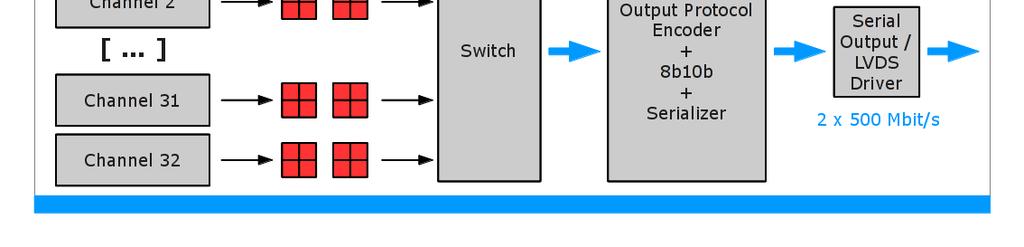
4 SPADIC 1.0 Overview 32 channels Per channel: Two CSAs (both polarities) pipeline ADC, ENOB ~ 8 bit IIR filter Autonomous hit detection Complex package builder Neighbor readout Time Stamp Readout: FIFO buffer per channel Preserved Timestamp-order Injection of Epoch Events CBMnet 2.0 protocol 2 LVDS 500Mbps 5 x 5mm 2, UMC 180nm P. Fischer, NSS 2012, Page 4


5 Data-Flow P. Fischer, NSS 2012, Page 5


6 Data-Flow P. Fischer, NSS 2012, Page 6
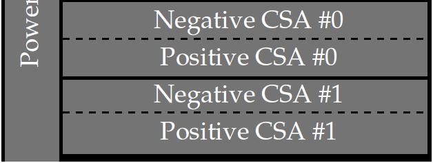
7 Charge Amplifiers Two CSAs: positive and negative polarity (input range 75 fc), single ended Shaping-time: 80ns (simple CR-RC shaper) Noise: 30pF (sim.), previous ASIC: 30pF (measured) Power: 4mW (positive), 10mW (negative, not optimized) Layout: 440µm x 60 µm (each polarity) Features: Power disable, modular & scalable layouts and schematics P. Fischer, NSS 2012, Page 7

8 Charge Amplifiers P. Fischer, NSS 2012, Page 8
9 Charge Amplifier Output Signals Measured via monitor bus (slow, noisy) as a proof of operation Negative polarity FE Positive polarity FE P. Fischer, NSS 2012, Page 9

10 ADC Pipelined Design using Current Mode Storage cells Bit 2 Bit Low input impedance Integrator detects residual input current Current threshold Transconductor generates current Replicas generate current copy P. Fischer, NSS 2012, Page 10
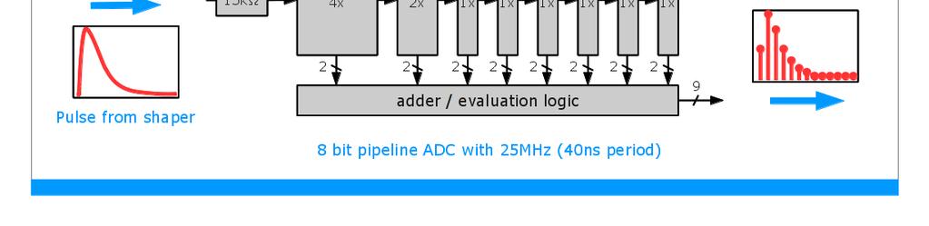
11 Pipeline ADC Signal doubling by use of 2 storage cells / stage & current addition Noise of first stages is decreased by higher power there 8 pipeline stages of 1.5 bit with error correction 9 bit (ENOB ~8), 25 MS/s, 4.8 mw. Rad-hard layout, Size: 400 x 300 µm 2 P. Fischer, NSS 2012, Page 11
12 Pipeline ADC Transfer Measured at 20 MSps, 9 Bit Mode ( ) red: average purple: 1 sigma P. Fischer, NSS 2012, Page 12

13 Pipeline ADC INL 20 MSps, 9 Bit mode: + 2 LSB - 2 LSB Limit of dynamic range red: average purple: 1 sigma P. Fischer, NSS 2012, Page 13

14 Digitized Pulses P. Fischer, NSS 2012, Page 14


15 IIR Filter Main Purposes Ion-tail cancellation (MWPC) Baseline stabilization Pulse inversion (required for negative front-end) Structure Four 1st order stages 25MHz max. Configuration/Simulation Software P. Fischer, NSS 2012, Page 15
 8 bit coefficients P. Fischer, NSS 2012, Page 16")
16 IIR Filter Optimization Determine quantization errors introduced by internal bit widths Choose bits width as small as possible to simplify the multipliers different bit widths Quantization Error for different filter settings vs. Bit width Our conclusion: 16 bit internal resolution (very generous) 8 bit coefficients P. Fischer, NSS 2012, Page 16
17 Ion Tail Cancellation / IIR Filter Simulation Input After filter P. Fischer, NSS 2012, Page 17
18 Ion Tail Cancellation / IIR Filter Simulation Shorter shaping P. Fischer, NSS 2012, Page 18


")
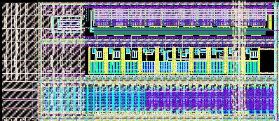
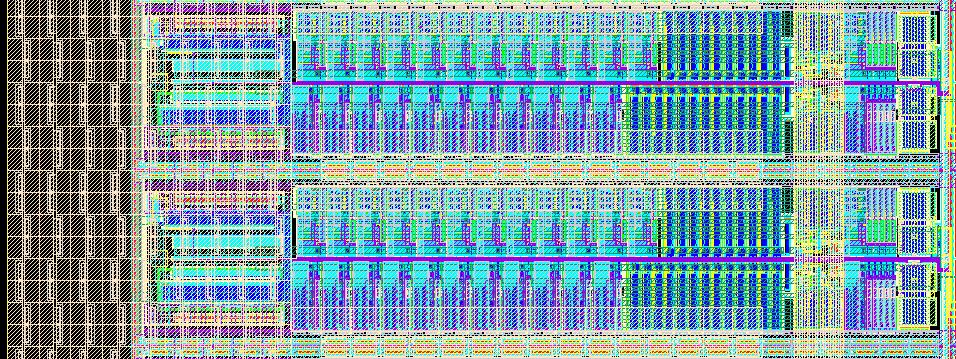
19 The Digital Part Cut-out: 14.4 µm x 5.76 µm (green: DFF) 250 MHz reference via CBMnet, other frequencies internally derived 3 CLK domains: 250 / 125 / 25 MHz 2.5 million transistors, 23k FF, 81k gates, total wire length: 14.4 m Home-made standard cell library 44 Faraday SRAMS (for FIFOs) Complete: 3.5 mm x 4.5 mm Power (@ 200 MHz): 600 mw P. Fischer, NSS 2012, Page 19


20 Hit Detector and Message Builder P. Fischer, NSS 2012, Page 20
21 Hit Selection Logic Allows to pick a set of interesting points in the pulse P. Fischer, NSS 2012, Page 21

 P.")
22 Message Format Definition Benefits: Very reliable definition (each word has a preamble) Bit-flips or loss of whole words are only a problem in the local context Message stream can always be re-synchronized, even if whole words are lost Large number of predefined messages (normal, epoch, info, error, warning, ) Easily adjustable/extendable Suitable for on-the-fly stream analysis (e.g. monitor time-stamps, count hits,...) P. Fischer, NSS 2012, Page 22

 Reliable Link: Retransmission, 8b/10b, CRC,... P.")
23 CBMnet Features: 2 x 500 Mbps downstream, 1 x 500 Mbps upstream (serial links, DDR) Automatic link initialization and management Only 4 LVDS pairs required (data, control and synchronization shared) Deterministic Latency Message: Fixed latency through network (sync, trigger,..) Reliable Link: Retransmission, 8b/10b, CRC,... P. Fischer, NSS 2012, Page 23


24 Channel Message Switch + Epoch Channel Epoch Events flag when time stamp counter wraps Epoch generation P. Fischer, NSS 2012, Page 24


25 SPADIC 1.0 Lab Setup P. Fischer, NSS 2012, Page 25
26 First Full System Measurement + IIR Using Spadic 1.0 and readout system 20 Msamples/s red: test pulses green: IIR enabled (configuration on first guess) P. Fischer, NSS 2012, Page 26
27 Summary & Outlook Spadic is a System on a Chip for self triggered charge readout Flexible Data Processing IIR Filter Threshold options Neighbour trigger Programmable pulse pattern Time ordered readout & epoch markers It implements CBMNet Deterministic Latency Messages & Data & Control over a single link. It includes acknowledge & retransmission of data. Status Chip & CBMNet are being commissioned. Everything works so far. Chip will be used for Detector tests & beam test soon P. Fischer, NSS 2012, Page 27
28 Funded by German BMBF under Contract # 06HD9120l SPADIC A Multi Channel Charge Digitizier & Processing ASIC 28
SPADIC Status and plans
 SPADIC Status and plans Michael Krieger TRD Strategy Meeting 29.11.2013 Michael Krieger SPADIC Status and plans 1 Reminder: SPADIC 1.0 architecture from detector pads single message stream: signal snapshot
SPADIC 1.0. Tim Armbruster. FEE/DAQ Workshop Mannheim. January Visit
 SPADIC 1.0 Tim Armbruster tim.armbruster@ziti.uni-heidelberg.de FEE/DAQ Workshop Mannheim Schaltungstechnik Schaltungstechnik und und January 2012 Visit http://www.spadic.uni-hd.de 1. SPADIC Architecture
SPADIC v0.3 and v1.0
 SPADIC v0.3 and v1.0 Self-triggered Pulse Amplification and Digitization asic Tim Armbruster tim.armbruster@ziti.uni-heidelberg.de FEE/DAQ Meeting @ FIAS (Frankfurt) Schaltungstechnik Schaltungstechnik
Status of Front End Development
 Status of Front End Development Progress of CSA and ADC studies Tim Armbruster tim.armbruster@ziti.uni-heidelberg.de CBM-XYTER Family Planning Workshop Schaltungstechnik und 05.12.2008 Introduction Previous
Motivation Overview Grounding & Shielding L1 Trigger System Diagrams Front-End Electronics Modules
 F.J. Barbosa, Jlab 1. 2. 3. 4. 5. 6. 7. 8. 9. Motivation Overview Grounding & Shielding L1 Trigger System Diagrams Front-End Electronics Modules Safety Summary 1 1. Motivation Hall D will begin operations
Algorithmic Pipeline ADC
 Algorithmic Pipeline ADC Ivan Perić's new current-mode ADC design Tim Armbruster tim.armbruster@ziti.uni-heidelberg.de 13th CBM CM Darmstadt Schaltungstechnik und 1.03.009 ADC Overview and Application
Firmware development and testing of the ATLAS IBL Read-Out Driver card
 Firmware development and testing of the ATLAS IBL Read-Out Driver card *a on behalf of the ATLAS Collaboration a University of Washington, Department of Electrical Engineering, Seattle, WA 98195, U.S.A.
A Readout ASIC for CZT Detectors
 A Readout ASIC for CZT Detectors L.L.Jones a, P.Seller a, I.Lazarus b, P.Coleman-Smith b a STFC Rutherford Appleton Laboratory, Didcot, OX11 0QX, UK b STFC Daresbury Laboratory, Warrington WA4 4AD, UK
A radiation tolerant, low-power cryogenic capable CCD readout system:
 A radiation tolerant, low-power cryogenic capable CCD readout system: Enabling focal-plane mounted CCD read-out for ground or space applications with a pair of ASICs. Overview What do we want to read out
A Prototype Amplifier-Discriminator Chip for the GLAST Silicon-Strip Tracker
 A Prototype Amplifier-Discriminator Chip for the GLAST Silicon-Strip Tracker Robert P. Johnson Pavel Poplevin Hartmut Sadrozinski Ned Spencer Santa Cruz Institute for Particle Physics The GLAST Project
Development of Radiation-Hard ASICs for the ATLAS Phase-1 Liquid Argon Calorimeter Readout Electronics Upgrade
 Development of Radiation-Hard ASICs for the ATLAS Phase-1 Liquid Argon Calorimeter Readout Electronics Upgrade Tim Andeen*, Jaroslav BAN, Nancy BISHOP, Gustaaf BROOIJMANS, Alex EMERMAN,Ines OCHOA, John
Noise Performance Analysis for the Silicon Tracking System Detector and Front-End Electronics
 Noise Performance Analysis for the Silicon Tracking System Detector and Front-End Electronics Weronika Zubrzycka, Krzysztof Kasiński zubrzycka@agh.edu.pl, kasinski@agh.edu.pl Department of Measurement
Final Results from the APV25 Production Wafer Testing
 Final Results from the APV Production Wafer Testing M.Raymond a, R.Bainbridge a, M.French b, G.Hall a, P. Barrillon a a Blackett Laboratory, Imperial College, London, UK b Rutherford Appleton Laboratory,
CBC3 status. Tracker Upgrade Week, 10 th March, 2017
 CBC3 status Tracker Upgrade Week, 10 th March, 2017 Mark Raymond, Imperial College Mark Prydderch, Michelle Key-Charriere, Lawrence Jones, Stephen Bell, RAL 1 introduction CBC3 is the final prototype front
Status of Front-end chip development at Paris ongoing R&D at LPNHE-Paris
 Status of Front-end chip development at Paris ongoing R&D at LPNHE-Paris Paris in the framework of the SiLC R&D Collaboration Jean-Francois Genat, Thanh Hung Pham, Herve Lebbolo, Marc Dhellot and Aurore
A 4 Channel Waveform Sampling ASIC in 130 nm CMOS
 A 4 Channel Waveform Sampling ASIC in 130 nm CMOS E. Oberla, H. Grabas, J.F. Genat, H. Frisch Enrico Fermi Institute, University of Chicago K. Nishimura, G. Varner University of Hawai I Large Area Picosecond
KLauS4: A Multi-Channel SiPM Charge Readout ASIC in 0.18 µm UMC CMOS Technology
 1 KLauS: A Multi-Channel SiPM Charge Readout ASIC in 0.18 µm UMC CMOS Technology Z. Yuan, K. Briggl, H. Chen, Y. Munwes, W. Shen, V. Stankova, and H.-C. Schultz-Coulon Kirchhoff Institut für Physik, Heidelberg
Test Measurements with the Hit-Detection ASIC V2.00 for the APFEL Preamplifier
 Test Measurements with the Hit-Detection ASIC V2.00 for the APFEL Preamplifier L. Capozza, H. Deppe, H. Flemming, P. Grasemann, O. Noll, P. Wieczorek Helmholtz-Institut Mainz PANDA Collaboration Meeting
A 4-Channel Fast Waveform Sampling ASIC in 130 nm CMOS
 A 4-Channel Fast Waveform Sampling ASIC in 130 nm CMOS E. Oberla, H. Grabas, M. Bogdan, J.F. Genat, H. Frisch Enrico Fermi Institute, University of Chicago K. Nishimura, G. Varner University of Hawai I
Towards an ADC for the Liquid Argon Electronics Upgrade
 1 Towards an ADC for the Liquid Argon Electronics Upgrade Gustaaf Brooijmans Upgrade Workshop, November 10, 2009 2 Current LAr FEB Existing FEB (radiation tolerant for LHC, but slhc?) Limits L1 latency
The High-Voltage Monolithic Active Pixel Sensor for the Mu3e Experiment
 The High-Voltage Monolithic Active Pixel Sensor for the Mu3e Experiment Shruti Shrestha On Behalf of the Mu3e Collaboration International Conference on Technology and Instrumentation in Particle Physics
managed by Brookhaven Science Associates for the U.S. Department of Energy VMM1 Front-end ASIC for charge-interpolating micro-pattern gas detectors
 managed by Brookhaven Science Associates for the U.S. Department of Energy VMM1 Front-end ASIC for charge-interpolating micro-pattern gas detectors Gianluigi De Geronimo Instrumentation Division, BNL April
Development of an analog read-out channel for time projection chambers
 Journal of Physics: Conference Series PAPER OPEN ACCESS Development of an analog read-out channel for time projection chambers To cite this article: E Atkin and I Sagdiev 2017 J. Phys.: Conf. Ser. 798
A 130nm CMOS Evaluation Digitizer Chip for Silicon Strips readout at the ILC
 A 130nm CMOS Evaluation Digitizer Chip for Silicon Strips readout at the ILC Jean-Francois Genat Thanh Hung Pham on behalf of W. Da Silva 1, J. David 1, M. Dhellot 1, D. Fougeron 2, R. Hermel 2, J-F. Huppert
ASYNCHRONOUS FRONT-END ASIC FOR X-RAY MEDICAL IMAGING APPLICATIONS IMPLEMENTED IN CMOS 0.18μm TECHNOLOGY R. DLUGOSZ 1
 ASYNCHRONOUS FRONT-D ASIC FOR X-RAY MEDICAL IMAGING APPLICATIONS IMPLEMTED IN CMOS 0.18μm TECHNOLOGY R. DLUGOSZ 1 UNIVERSITY OF NEUCHÂTEL, SWITZERLAND 2 UNIVERSITY OF ALBERTA, CANADA KEYWORDS: X-ray medical
Readout Electronics. P. Fischer, Heidelberg University. Silicon Detectors - Readout Electronics P. Fischer, ziti, Uni Heidelberg, page 1
 Readout Electronics P. Fischer, Heidelberg University Silicon Detectors - Readout Electronics P. Fischer, ziti, Uni Heidelberg, page 1 We will treat the following questions: 1. How is the sensor modeled?
THE LHCb experiment [1], currently under construction
![THE LHCb experiment [1], currently under construction](/thumbs/92/108383532.jpg "THE LHCb experiment [1], currently under construction") The DIALOG Chip in the Front-End Electronics of the LHCb Muon Detector Sandro Cadeddu, Caterina Deplano and Adriano Lai, Member, IEEE Abstract We present a custom integrated circuit, named DI- ALOG, which
The DIALOG Chip in the Front-End Electronics of the LHCb Muon Detector Sandro Cadeddu, Caterina Deplano and Adriano Lai, Member, IEEE Abstract We present a custom integrated circuit, named DI- ALOG, which
A Low-Offset Latched Comparator Using Zero-Static Power Dynamic Offset Cancellation Technique
 1 A Low-Offset Latched Comparator Using Zero-Static Power Dynamic Offset Cancellation Technique Masaya Miyahara and Akira Matsuzawa Tokyo Institute of Technology, Japan 2 Outline Motivation Design Concept
Detectors (on sphere) Neutron Source (Reactor) Chopper (TOF->E) Neutron Beam (non-monochromatic) Target x-rays (Background)
 Neutron Source (Reactor) Chopper (TOF->E) Neutron Beam (non-monochromatic) Target x-rays (Background)") n-xyter - A CMOS Read-Out ASIC for a new Generation of High Rate Multichannel Counting Mode Neutron Detectors A.S. Brogna a,c, S. Buzzetti a,d, W. Dabrowski b, T. Fiutowski b, B. Gebauer c,m.klein a, C.J.
n-xyter - A CMOS Read-Out ASIC for a new Generation of High Rate Multichannel Counting Mode Neutron Detectors A.S. Brogna a,c, S. Buzzetti a,d, W. Dabrowski b, T. Fiutowski b, B. Gebauer c,m.klein a, C.J.
How different FPGA firmware options enable digitizer platforms to address and facilitate multiple applications
 How different FPGA firmware options enable digitizer platforms to address and facilitate multiple applications 1 st of April 2019 Marc.Stackler@Teledyne.com March 19 1 Digitizer definition and application
A 4 GSample/s 8-bit ADC in. Ken Poulton, Robert Neff, Art Muto, Wei Liu, Andrew Burstein*, Mehrdad Heshami* Agilent Laboratories Palo Alto, California
 A 4 GSample/s 8-bit ADC in 0.35 µm CMOS Ken Poulton, Robert Neff, Art Muto, Wei Liu, Andrew Burstein*, Mehrdad Heshami* Agilent Laboratories Palo Alto, California 1 Outline Background Chip Architecture
Front-End and Readout Electronics for Silicon Trackers at the ILC
 2005 International Linear Collider Workshop - Stanford, U.S.A. Front-End and Readout Electronics for Silicon Trackers at the ILC M. Dhellot, J-F. Genat, H. Lebbolo, T-H. Pham, and A. Savoy Navarro LPNHE
Commissioning Status and Results of ATLAS Level1 Endcap Muon Trigger System. Yasuyuki Okumura. Nagoya TWEPP 2008
 Commissioning Status and Results of ATLAS Level1 Endcap Muon Trigger System Yasuyuki Okumura Nagoya University @ TWEPP 2008 ATLAS Trigger DAQ System Trigger in LHC-ATLAS Experiment 3-Level Trigger System
Overview 256 channel Silicon Photomultiplier large area using matrix readout system The SensL Matrix detector () is the largest area, highest channel
 is the largest area, highest channel") 技股份有限公司 wwwrteo 公司 wwwrteo.com Page 1 Overview 256 channel Silicon Photomultiplier large area using matrix readout system The SensL Matrix detector () is the largest area, highest channel count, Silicon
技股份有限公司 wwwrteo 公司 wwwrteo.com Page 1 Overview 256 channel Silicon Photomultiplier large area using matrix readout system The SensL Matrix detector () is the largest area, highest channel count, Silicon
SAMPA ASIC and Test Stand. TDIS Workshop - 2/22/18 Ed Jastrzembski DAQ Group
 SAMPA ASIC and Test Stand TDIS Workshop - 2/22/18 Ed Jastrzembski DAQ Group 1 SAMPA - nickname for the city of São Paulo, Brazil New ASIC for the ALICE TPC and Muon Chamber (MCH) upgrades Combines functions
PARISROC, a Photomultiplier Array Integrated Read Out Chip
 PARISROC, a Photomultiplier Array Integrated Read Out Chip S. Conforti Di Lorenzo a, J.E. Campagne b, F. Dulucq a, C. de La Taille a, G. Martin-Chassard a, M. El Berni a, W. Wei c a OMEGA/LAL/IN2P3, centre
Status of SVT front-end electronics M. Citterio on behalf of INFN and University of Milan
 XVII SuperB Workshop and Kick Off Meeting: ETD3 Parallel Session Status of SVT front-end electronics M. Citterio on behalf of INFN and University of Milan Index SVT: system status Parameter space Latest
GBT based readout in the CBM experiment
 CBM GBT based readout in the CBM experiment J. Lehnert (GSI Darmstadt) for the CBM Collaboration TWEPP 2016 - Topical Workshop on Electronics in Particle Physics Karlsruhe Institute of Technology Wed.
Calorimetry in particle physics experiments
 Calorimetry in particle physics experiments Unit n. 7 Front End and Trigger electronics Roberta Arcidiacono Lecture overview Signal processing Some info on calorimeter FE Pre-amplifiers Charge sensitive
CATIROC a multichannel front-end ASIC to read out the SPMT system of the JUNO experiment
 CATIROC a multichannel front-end ASIC to read out the SPMT system of the JUNO experiment Dr. Selma Conforti (OMEGA/IN2P3/CNRS) OMEGA microelectronics group Ecole Polytechnique & CNRS IN2P3 http://omega.in2p3.fr
The Concept of LumiCal Readout Electronics
 EUDET The Concept of LumiCal Readout Electronics M. Idzik, K. Swientek, Sz. Kulis, W. Dabrowski, L. Suszycki, B. Pawlik, W. Wierba, L. Zawiejski on behalf of the FCAL collaboration July 4, 7 Abstract The
Prototype of a Compact Imaging System for GEM Detectors Tomohisa Uchida, Member, IEEE, Yowichi Fujita, Manobu Tanaka, Member, IEEE, and Shoji Uno
 2698 IEEE TRANSACTIONS ON NUCLEAR SCIENCE, VOL. 55, NO. 5, OCTOBER 2008 Prototype of a Compact Imaging System for GEM Detectors Tomohisa Uchida, Member, IEEE, Yowichi Fujita, Manobu Tanaka, Member, IEEE,
Noise Characteristics Of The KPiX ASIC Readout Chip
 Noise Characteristics Of The KPiX ASIC Readout Chip Cabrillo College Stanford Linear Accelerator Center What Is The ILC The International Linear Collider is an e- e+ collider Will operate at 500GeV with
CHAPTER 8 PHOTOMULTIPLIER TUBE MODULES
 CHAPTER 8 PHOTOMULTIPLIER TUBE MODULES This chapter describes the structure, usage, and characteristics of photomultiplier tube () modules. These modules consist of a photomultiplier tube, a voltage-divider
Data Acquisition System for the Angra Project
 Angra Neutrino Project AngraNote 012-2009 (Draft) Data Acquisition System for the Angra Project H. P. Lima Jr, A. F. Barbosa, R. G. Gama Centro Brasileiro de Pesquisas Físicas - CBPF L. F. G. Gonzalez
A single-slope 80MS/s ADC using two-step time-to-digital conversion
 A single-slope 80MS/s ADC using two-step time-to-digital conversion The MIT Faculty has made this article openly available. Please share how this access benefits you. Your story matters. Citation As Published
Technology Timeline. Transistors ICs (General) SRAMs & DRAMs Microprocessors SPLDs CPLDs ASICs. FPGAs. The Design Warrior s Guide to.
 SRAMs & DRAMs Microprocessors SPLDs CPLDs ASICs. FPGAs. The Design Warrior s Guide to.") FPGAs 1 CMPE 415 Technology Timeline 1945 1950 1955 1960 1965 1970 1975 1980 1985 1990 1995 2000 Transistors ICs (General) SRAMs & DRAMs Microprocessors SPLDs CPLDs ASICs FPGAs The Design Warrior s Guide
FPGAs 1 CMPE 415 Technology Timeline 1945 1950 1955 1960 1965 1970 1975 1980 1985 1990 1995 2000 Transistors ICs (General) SRAMs & DRAMs Microprocessors SPLDs CPLDs ASICs FPGAs The Design Warrior s Guide
The Architecture of the BTeV Pixel Readout Chip
 The Architecture of the BTeV Pixel Readout Chip D.C. Christian, dcc@fnal.gov Fermilab, POBox 500 Batavia, IL 60510, USA 1 Introduction The most striking feature of BTeV, a dedicated b physics experiment
MAPS-based ECAL Option for ILC
 MAPS-based ECAL Option for ILC, Spain Konstantin Stefanov On behalf of J. Crooks, P. Dauncey, A.-M. Magnan, Y. Mikami, R. Turchetta, M. Tyndel, G. Villani, N. Watson, J. Wilson v Introduction v ECAL with
CALICE AHCAL overview
 International Workshop on the High Energy Circular Electron-Positron Collider in 2018 CALICE AHCAL overview Yong Liu (IHEP), on behalf of the CALICE collaboration Nov. 13, 2018 CALICE-AHCAL Progress, CEPC
The ALTRO Chip: A 16-Channel A/D Converter and Digital Processor for Gas Detectors
 2460 IEEE TRANSACTIONS ON NUCLEAR SCIENCE, VOL. 50, NO. 6, DECEMBER 2003 The ALTRO Chip: A 16-Channel A/D Converter and Digital Processor for Gas Detectors R. Esteve Bosch, A. Jiménez de Parga, B. Mota,
MASE: Multiplexed Analog Shaped Electronics
 MASE: Multiplexed Analog Shaped Electronics C. Metelko, A. Alexander, J. Poehlman, S. Hudan, R.T. desouza Outline 1. Needs 2. Problems with existing Technology 3. Design Specifications 4. Overview of the
Nyquist filter FIFO. Amplifier. Impedance matching. 40 MHz sampling ADC. DACs for gain and offset FPGA. clock distribution (not yet implemented)
") The Digital Gamma Finder (DGF) Firewire clock distribution (not yet implemented) DSP One of four channels Inputs Camac for 4 channels 2 cm System FPGA Digital part Analog part FIFO Amplifier Nyquist filter
The Digital Gamma Finder (DGF) Firewire clock distribution (not yet implemented) DSP One of four channels Inputs Camac for 4 channels 2 cm System FPGA Digital part Analog part FIFO Amplifier Nyquist filter
TIMING, TRIGGER AND CONTROL INTERFACE MODULE FOR ATLAS SCT READ OUT ELECTRONICS
 TIMING, TRIGGER AND CONTROL INTERFACE MODULE FOR ATLAS SCT READ OUT ELECTRONICS Jonathan Butterworth ( email : jmb@hep.ucl.ac.uk ) Dominic Hayes ( email : dah@hep.ucl.ac.uk ) John Lane ( email : jbl@hep.ucl.ac.uk
Module -18 Flip flops
 1 Module -18 Flip flops 1. Introduction 2. Comparison of latches and flip flops. 3. Clock the trigger signal 4. Flip flops 4.1. Level triggered flip flops SR, D and JK flip flops 4.2. Edge triggered flip
An Analog Phase-Locked Loop
 1 An Analog Phase-Locked Loop Greg Flewelling ABSTRACT This report discusses the design, simulation, and layout of an Analog Phase-Locked Loop (APLL). The circuit consists of five major parts: A differential
A Low-Power 6-b Integrating-Pipeline Hybrid Analog-to-Digital Converter
 A Low-Power 6-b Integrating-Pipeline Hybrid Analog-to-Digital Converter Quentin Diduck, Martin Margala * Electrical and Computer Engineering Department 526 Computer Studies Bldg., PO Box 270231 University
Implementation of A Nanosecond Time-resolved APD Detector System for NRS Experiment in HEPS-TF
 Implementation of A Nanosecond Time-resolved APD Detector System for NRS Experiment in HEPS-TF LI Zhen-jie a ; MA Yi-chao c ; LI Qiu-ju a ; LIU Peng a ; CHANG Jin-fan b ; ZHOU Yang-fan a * a Beijing Synchrotron
Picosecond time measurement using ultra fast analog memories.
 Picosecond time measurement using ultra fast analog memories. Dominique Breton a, Eric Delagnes b, Jihane Maalmi a acnrs/in2p3/lal-orsay, bcea/dsm/irfu breton@lal.in2p3.fr Abstract The currently existing
A new Readout Chip for LHCb. Beetle Daniel Baumeister, Werner Hofmann, Karl-Tasso Knöpfle, Sven Löchner, Michael Schmelling, Edgar Sexauer
 ASIC-Labor Heidelberg ASIC-Labor Heidelberg Beetle 1.0 - A new Readout Chip for LHCb Daniel Baumeister, Werner Hofmann, Karl-Tasso Knöpfle, Sven Löchner, Michael Schmelling, Max-Planck-Institute for Nuclear
Hello, and welcome to this presentation of the STM32 Digital Filter for Sigma-Delta modulators interface. The features of this interface, which
 Hello, and welcome to this presentation of the STM32 Digital Filter for Sigma-Delta modulators interface. The features of this interface, which behaves like ADC with external analog part and configurable
The Medipix3 Prototype, a Pixel Readout Chip Working in Single Photon Counting Mode with Improved Spectrometric Performance
 26 IEEE Nuclear Science Symposium Conference Record NM1-6 The Medipix3 Prototype, a Pixel Readout Chip Working in Single Photon Counting Mode with Improved Spectrometric Performance R. Ballabriga, M. Campbell,
GPU-accelerated SDR Implementation of Multi-User Detector for Satellite Return Links
 DLR.de Chart 1 GPU-accelerated SDR Implementation of Multi-User Detector for Satellite Return Links Chen Tang chen.tang@dlr.de Institute of Communication and Navigation German Aerospace Center DLR.de Chart
Status of TPC-electronics with Time-to-Digit Converters
 EUDET Status of TPC-electronics with Time-to-Digit Converters A. Kaukher, O. Schäfer, H. Schröder, R. Wurth Institut für Physik, Universität Rostock, Germany 31 December 2009 Abstract Two components of
A Low-Noise Self-Calibrating Dynamic Comparator for High-Speed ADCs
 1 A Low-Noise Self-Calibrating Dynamic Comparator for High-Speed ADCs Masaya Miyahara, Yusuke Asada, Daehwa Paik and Akira Matsuzawa Tokyo Institute of Technology, Japan Outline 2 Motivation The Calibration
A 0.55 V 7-bit 160 MS/s Interpolated Pipeline ADC Using Dynamic Amplifiers
 A 0.55 V 7-bit 160 MS/s Interpolated Pipeline ADC Using Dynamic Amplifiers James Lin, Daehwa Paik, Seungjong Lee, Masaya Miyahara, and Akira Matsuzawa Tokyo Institute of Technology, Japan Matsuzawa & Okada
Helicity Clock Generator
 Helicity Clock Generator R. Wojcik, N. Sinkin, C. Yan Jefferson Lab, 12000 Jefferson Ave, Newport News, VA 23606 Tech Note: JLAB-TN-01-035 ABSTRACT Based on the phased-locked loop (PLL) technique, a versatile
Readout electronics for LumiCal detector
 Readout electronics for Lumial detector arek Idzik 1, Krzysztof Swientek 1 and Szymon Kulis 1 1- AGH niversity of Science and Technology Faculty of Physics and Applied omputer Science racow - Poland The
ADC Board 4 Channel Notes September 29, DRAFT - May not be correct
 ADC Board 4 Channel Notes September 29, 2006 - DRAFT - May not be correct Board Features 4 Chan - 130MSPS 16 bit ADCs LTC2208 - Data clocked into 64k Sample FIFOs 1 buffered clock input to CPLD 1 buffered
MTJ based Random Number Generation and Analog-to-Digital Conversion Chris H. Kim University of Minnesota
 MTJ based Random Number Generation and Analog-to-Digital Conversion Chris H. Kim University of Minnesota Workshop on the Future of Spintronics, June 5, 216 1 Switching Probability of an MTJ Parallel: Low
A Fast Waveform-Digitizing ASICbased DAQ for a Position & Time Sensing Large-Area Photo-Detector System
 A Fast Waveform-Digitizing ASICbased DAQ for a Position & Time Sensing Large-Area Photo-Detector System Eric Oberla on behalf of the LAPPD collaboration PHOTODET 2012 12-June-2012 Outline LAPPD overview:
INTEGRATED CIRCUITS. For a complete data sheet, please also download:
 INTEGRATED CIRCUITS DATA SHEET For a complete data sheet, please also download: The IC06 74HC/HCT/HCU/HCMOS Logic Family Specifications The IC06 74HC/HCT/HCU/HCMOS Logic Package Information The IC06 74HC/HCT/HCU/HCMOS
Digital Controller Chip Set for Isolated DC Power Supplies
 Digital Controller Chip Set for Isolated DC Power Supplies Aleksandar Prodic, Dragan Maksimovic and Robert W. Erickson Colorado Power Electronics Center Department of Electrical and Computer Engineering
Another way to implement a folding ADC
 Another way to implement a folding ADC J. Van Valburg and R. van de Plassche, An 8-b 650 MHz Folding ADC, IEEE JSSC, vol 27, #12, pp. 1662-6, Dec 1992 Coupled Differential Pair J. Van Valburg and R. van
EITF35: Introduction to Structured VLSI Design
 EITF35: Introduction to Structured VLSI Design Part 4.2.1: Learn More Liang Liu liang.liu@eit.lth.se 1 Outline Crossing clock domain Reset, synchronous or asynchronous? 2 Why two DFFs? 3 Crossing clock
Exercise 3: Sound volume robot
 ETH Course 40-048-00L: Electronics for Physicists II (Digital) 1: Setup uc tools, introduction : Solder SMD Arduino Nano board 3: Build application around ATmega38P 4: Design your own PCB schematic 5:
Analog Peak Detector and Derandomizer
 Analog Peak Detector and Derandomizer G. De Geronimo, A. Kandasamy, P. O Connor Brookhaven National Laboratory IEEE Nuclear Sciences Symposium, San Diego November 7, 2001 Multichannel Readout Alternatives
Highly Segmented Detector Arrays for. Studying Resonant Decay of Unstable Nuclei. Outline
 Highly Segmented Detector Arrays for Studying Resonant Decay of Unstable Nuclei MASE: Multiplexed Analog Shaper Electronics C. Metelko, S. Hudan, R.T. desouza Outline 1. Resonant Decay 2. Detectors 3.
Helicity Clock Generator
 Helicity Clock Generator R. Wojcik, N. Sinkin, C. Yan Jefferson Lab, 12000 Jefferson Ave, Newport News, VA 23606 Tech Note: JLAB-TN-01-035 ABSTRACT Based on the phased-locked loop (PLL) technique, a versatile
ADC Measurements PARISROC Chip. Selma Conforti Di Lorenzo OMEGA/LAL Orsay
 ADC Measurements PARISROC Chip Selma Conforti Di Lorenzo OMEGA/LAL Orsay PARISROC ADC Measurements Ecole Microélectronique_11/16 octobre 2009 conforti@lal.in2p3.fr 2 TEST BOARD TEST BENCH ASIC FPGA USB
IMPLEMENTING THE 10-BIT, 50MS/SEC PIPELINED ADC
 98 CHAPTER 5 IMPLEMENTING THE 0-BIT, 50MS/SEC PIPELINED ADC 99 5.0 INTRODUCTION This chapter is devoted to describe the implementation of a 0-bit, 50MS/sec pipelined ADC with different stage resolutions
TPC Readout with GEMs & Pixels
 TPC Readout with GEMs & Pixels + Linear Collider Tracking Directional Dark Matter Detection Directional Neutron Spectroscopy? Sven Vahsen Lawrence Berkeley Lab Cygnus 2009, Cambridge Massachusetts 2 Our
LPFilter: Exponential Moving Average Digital Filter 0.0. Features. General description
 PSoC Creator Component datasheet LPFilter: Exponential Moving Average Digital Filter. Features Implements exponential moving average digital filter. Arbitrary ut and ut bus width. Variable dumping length.
ITk silicon strips detector test beam at DESY
 ITk silicon strips detector test beam at DESY Lucrezia Stella Bruni Nikhef Nikhef ATLAS outing 29/05/2015 L. S. Bruni - Nikhef 1 / 11 Qualification task I Participation at the ITk silicon strip test beams
Level-1 Calorimeter Trigger Calibration
 December 2004 Level-1 Calorimeter Trigger Calibration Birmingham, Heidelberg, Mainz, Queen Mary, RAL, Stockholm Alan Watson, University of Birmingham Norman Gee, Rutherford Appleton Lab Outline Reminder
EE247 Lecture 23. Advanced calibration techniques. Compensating inter-stage amplifier non-linearity Calibration via parallel & slow ADC
 EE247 Lecture 23 Pipelined ADCs Combining the bits Stage implementation Circuits Noise budgeting Advanced calibration techniques Compensating inter-stage amplifier non-linearity Calibration via parallel
ECEN 474/704 Lab 7: Operational Transconductance Amplifiers
 ECEN 474/704 Lab 7: Operational Transconductance Amplifiers Objective Design, simulate and layout an operational transconductance amplifier. Introduction The operational transconductance amplifier (OTA)
Mohit Arora. The Art of Hardware Architecture. Design Methods and Techniques. for Digital Circuits. Springer
 Mohit Arora The Art of Hardware Architecture Design Methods and Techniques for Digital Circuits Springer Contents 1 The World of Metastability 1 1.1 Introduction 1 1.2 Theory of Metastability 1 1.3 Metastability
Proposing. An Interpolated Pipeline ADC
 Proposing An Interpolated Pipeline ADC Akira Matsuzawa Tokyo Institute of Technology, Japan Matsuzawa & Okada Lab. Background 38GHz long range mm-wave system Role of long range mm-wave Current Optical
A NOVEL FPGA-BASED DIGITAL APPROACH TO NEUTRON/ -RAY PULSE ACQUISITION AND DISCRIMINATION IN SCINTILLATORS
 10th ICALEPCS Int. Conf. on Accelerator & Large Expt. Physics Control Systems. Geneva, 10-14 Oct 2005, PO2.041-4 (2005) A NOVEL FPGA-BASED DIGITAL APPROACH TO NEUTRON/ -RAY PULSE ACQUISITION AND DISCRIMINATION
Fast CMOS Transimpedance Amplifier and Comparator circuit for readout of silicon strip detectors at LHC experiments
 Fast CMOS Transimpedance Amplifier and Comparator circuit for readout of silicon strip detectors at LHC experiments Jan Kaplon - CERN Wladek Dabrowski - FPN/UMM Cracow Pepe Bernabeu IFIC Valencia Carlos
P14155A: 128 Channel Cross-correlator ASIC Datasheet Rev 2.1
 SUMMARY P14155A is a cross-correlator ASIC, featuring a digital correlation matrix and on-chip 2-bit 1GS/s digitization of 128 analog inputs. Cross-correlation results in 4096 products plus 512 totalizers
Comparison between Analog and Digital Current To PWM Converter for Optical Readout Systems
 Comparison between Analog and Digital Current To PWM Converter for Optical Readout Systems 1 Eun-Jung Yoon, 2 Kangyeob Park, 3* Won-Seok Oh 1, 2, 3 SoC Platform Research Center, Korea Electronics Technology
Design of the Front-End Readout Electronics for ATLAS Tile Calorimeter at the slhc
 IEEE TRANSACTIONS ON NUCLEAR SCIENCE, VOL. 60, NO. 2, APRIL 2013 1255 Design of the Front-End Readout Electronics for ATLAS Tile Calorimeter at the slhc F. Tang, Member, IEEE, K. Anderson, G. Drake, J.-F.
Requirements and Specifications of the TDC for the ATLAS Precision Muon Tracker
 ATLAS Internal Note MUON-NO-179 14 May 1997 Requirements and Specifications of the TDC for the ATLAS Precision Muon Tracker Yasuo Arai KEK, National High Energy Accelerator Research Organization Institute
Multi-channel front-end board for SiPM readout
 Preprint typeset in JINST style - HYPER VERSION Multi-channel front-end board for SiPM readout arxiv:1606.02290v1 [physics.ins-det] 7 Jun 2016 M. Auger, A. Ereditato, D. Goeldi, I. Kreslo, D. Lorca, M.
The Electronics Readout and Measurement of Parameters of. a Monitor System
 458 / 1004 The Electronics Readout and Measurement of Parameters of a Monitor System Abdolkazem Ansarinejad 1, Roberto Cirio 2 1 Physics and Accelerators School, Nuclear Science and Technology Research
GRETINA. Electronics. Auxiliary Detector Workshop. Sergio Zimmermann LBNL. Auxiliary Detectors Workshop. January 28, 2006
 GRETINA Auxiliary Detector Workshop Electronics Sergio Zimmermann LBNL 1 Outline Electronic Interface Options Digitizers Trigger/Timing System Grounding and Shielding Summary 2 Interface Options Three
Timing Issues in FPGA Synchronous Circuit Design
 ECE 428 Programmable ASIC Design Timing Issues in FPGA Synchronous Circuit Design Haibo Wang ECE Department Southern Illinois University Carbondale, IL 62901 1-1 FPGA Design Flow Schematic capture HDL
Development of Telescope Readout System based on FELIX for Testbeam Experiments
 Development of Telescope Readout System based on FELIX for Testbeam Experiments, Hucheng Chen, Kai Chen, Francessco Lanni, Hongbin Liu, Lailin Xu Brookhaven National Laboratory E-mail: weihaowu@bnl.gov,