Physical Design of a Smart Camera with Integrated Digital Pixel Sensors Using a 0.13µm 8-Layer Metal CMOS Process
|
|
|
- Owen Golden
- 5 years ago
- Views:
Transcription

1 University of Nebraska - Lincoln DigitalCommons@University of Nebraska - Lincoln Theses, Dissertations, and Student Research from Electrical & Computer Engineering Electrical & Computer Engineering, Department of Fall Physical Design of a Smart Camera with Integrated Digital Pixel Sensors Using a 0.13µm 8-Layer Metal CMOS Process Mahir K. Gharzai University of Nebraska-Lincoln, mkgharzai@gmail.com Follow this and additional works at: Part of the Electrical and Electronics Commons, Electronic Devices and Semiconductor Manufacturing Commons, and the VLSI and Circuits, Embedded and Hardware Systems Commons Gharzai, Mahir K., "Physical Design of a Smart Camera with Integrated Digital Pixel Sensors Using a 0.13µm 8-Layer Metal CMOS Process" (2013). Theses, Dissertations, and Student Research from Electrical & Computer Engineering This Article is brought to you for free and open access by the Electrical & Computer Engineering, Department of at DigitalCommons@University of Nebraska - Lincoln. It has been accepted for inclusion in Theses, Dissertations, and Student Research from Electrical & Computer Engineering by an authorized administrator of DigitalCommons@University of Nebraska - Lincoln.
2 PHYSICAL DESIGN OF A SMART CAMERA WITH INTEGRATED DIGITAL PIXEL SENSORS USING A 0.13 µm 8-LAYER METAL CMOS PROCESS by Mahir Kabeer Gharzai A THESIS Presented to the Faculty of The Graduate College at the University of Nebraska In Partial Fulfilment of Requirements For the Degree of Master of Science Major: Electrical Engineering Under the Supervision of Professor Sina Balkir Lincoln, Nebraska December, 2013
3 PHYSICAL DESIGN OF A SMART CAMERA WITH INTEGRATED DIGITAL PIXEL SENSORS USING A 0.13 µm 8-LAYER METAL CMOS PROCESS Mahir Kabeer Gharzai, M.S. University of Nebraska, 2013 Adviser: Sina Balkir The design of cameras has historically kept imagery and computational circuitry isolated in an attempt to maximize image quality by improving pixel pitch and routing density. Although this technique has worked in creating high density arrays of pixels for large resolution imagers, it has never been able to achieve high framerate computational operations. A radical approach is introduced to solve this dilemma by creating compact, lowpower pixel elements with built-in analog-to-digital converters that directly interface with digital logic. These pixels are capable of integrating alongside logic cells and to create an array of pixels inside the processor that can capture a scene and perform operations across the entire image in parallel. Minimization of electronic circuitry is explored to design exotic miniature logic cells to further compact the design and optimize imaging quality.
4 iii Contents List of Figures v 1 Smart Camera History What is a Smart Camera Chip-Level Imagers Column-Level Imagers Pixel-Level Imagers A Massively Parallel Smart Camera The Neighborhood Processor Migrating to Silicon Pixel Sensors Readout Schemes Schematic Design Design Considerations Schematic Drawing Layout Design Photodiode Design Considerations
5 iv 4.2 Antenna Rules Fill Rules Photodiode Layout NP Layout Top Layout Verification DRC LVS Area Minimization Techniques Custom Logic Cells DFF Layout Encounter Library Characterizer A Gated Clock Future Work Testbed DFF Test Structures Process Scaling Parallel Imagers Bibliography 39
6 v List of Figures 2.1 Photogate Pixel Photodiode Pixel Photodiode Acquisition Subthreshold Comparator Photodiode Schematic Photodiode Layout Analog Section Layout (M1 and below) Pins Along M3 Routing Channel Analog Routes NP Layout NP Layout Detail Top Layout Hierarchical Top Layout C 2 MOS DFF Design Transmission Gate DFF Design DFF Layout Ripple Counter
7 vi 6.5 NAND Test Structure DFF Test Structure
8 1 Chapter 1 Smart Camera History 1.1 What is a Smart Camera CMOS imaging arrays are silicon circuits that utilize structures on the substrate to convert photons to electric current. These structures contain readout circuitry to be able to interface with other portion of the chip, sometimes including converters or buffers. The combination of these is known as a pixel. CMOS technology has allowed other circuit elements to be placed alongside an array of pixels to perform a variety of operations such as compression, dynamic range adjustment, and object recognition. When such electronics are integrated directly onto silicon to perform processing operations in-chip, the camera is considered a Smart Camera. 1.2 Chip-Level Imagers The original technique for adding processing power to an imager array was to integrate processing circuitry separate, but nearby an imaging array. The processing circuitry was able to process data across the entire array of pixels but had to read
9 2 each value sequentially, slowing down operation. The flexibility of being able to program the processor to do a variety of operations was its primary appeal, even if high framerate operations were not possible. In addition to speed constraints, the chiplevel processing paradigm suffered from scalability issues. As imager sizes increased, processing speeds began to suffer due to the single processor having to manipulate data for an increasing amount of pixels. Framerates for simple operations remained limited to hundreds of frames per second. Computationally expensive operations, such as compression, were limited to tens of frames per second. 1.3 Column-Level Imagers As technlogies started to get more compact, around 0.25 µm and 0.18 µm, smaller feature sizes allowed simple circuitry to become embedded nearby pixels in the array. Simple computational operations requiring few transistors for functionality could be integrated at the row or column level of the imaging array to provide fast computation during readout [8]. Processing flexibility was lost due to having these operations hardcoded into the circuit, but processing speeds began to see an improvement. It was now possible to process data in the thousands of frames per second [2]. 1.4 Pixel-Level Imagers The final architecture explored in imaging arrays used in specialized applications embedded processing directly into pixels themselves. Technologies using feature sizes of 0.13 µm and below were finally able to include circuitry compact enough to fit in the array without increasing pixel pitch enough to destroy imaging quality. Pixel-level imagers sacrificed imaging quality for the pursuit of ultimate processing speed. Simple
10 3 operations achieved framerates in the tens of thousands of frames per second. Like the column-level processing architecture, pixel-level processing was also inflexible. Instructions had to be hardcoded and resulted in imagers that could only do a handful of tasks at incredible speeds [10].
11 4 Chapter 2 A Massively Parallel Smart Camera 2.1 The Neighborhood Processor In the work of a previous graduate student, Anantha Nelliparthi, a processor architecture was designed which could perform parallel operations and communicate with other processors in a neighborhood array [3]. The advantages from the chip, column, and pixel-level processing architectures were combined to create a flexible, high framerate imager with acceptable image quality. Each neighborhood processor (NP) contained 64 pixels and could perform a variety of operations in parallel across this small array. An array of NP s could be created of any size without sacrificing speed, due to the parallelism of the design. The design was verified on an FPGA platform demonstrating several imaging operations across the pixel array that showed promise of the NP s potential. In this work, the NP design is fully implemented in a 0.13 µm silicon technology to create a novel Smart Camera.
12 5 2.2 Migrating to Silicon Pixel Sensors The most fundamental step in pixel design involves the method of sensing photons at the silicon level. An established technique for this conversion is to charge a capacitance to a reset voltage and allow it to decay. The natural loss of the voltage across the capacitance from tunneling effects is modeled as a current, known as dark current. When photons collide with one of the surfaces of the capacitor they will cause more loss of the voltage across the capacitance due to recombination effects. This drop in voltage is modeled as a current as well, known as photocurrent. By monitoring the photocurrent across the capacitors of the pixel array, we can obtain an image and deduce brightness levels for each pixel. The two techniques used in detecting this photocurrent involve different methods of creating the capacitance. The first technique is known as photogate and uses the gate of a transistor as a capacitance, shown in Figure 2.1. A transmit transistor is created adjacent to the photogate to read out the value of the voltage across the capacitance. The gate material is made of polysilicon and is insulated from the substrate with a thin gate oxide. In technologies prior to 0.18 µm, the gate oxide was thick enough to not suffer significantly from tunneling effects which resulted in relatively small dark currents. As technologies began to shrink, photogate began to show poor imaging quality due to an increase in dark current caused by smaller gate oxide thicknesses. When gate area was increased to improve imaging quality and increase the amount of photons absorbed by the polysilicon, quantum efficiency and signal-to-noise ratio did not increase linearly [7]. This led to a movement away from photogate technology and the development of a new pixel design for modern technologies.


13 6 Figure 2.1: Photogate Pixel Figure 2.2: Photodiode Pixel The second technique for photon absorption, known as a photodiode, utilizes the capacitance of the reverse biased diode created by P and N junctions, shown in Figure 2.2. An N-well is charged to a reset voltage and its capacitance across the substrate due to bulk and sidewall terms is allowed to leak. Due to the N-well s increased perimeter and area than the photogate, it has an improvement in quantum efficiency and signal-to-noise ratio that make it appealing for small feature sized technologies that need high quality imaging. Additionally, the photodiode scales very well with N-well size, allowing larger pixel fill to capture significantly more photons primarily due to an increase in perimeter area for larger N-wells. The advantages of the photodiode and its imaging performance in the 0.13 µm technology make it the superior technique for use in the neighborhood processor.
14 Readout Schemes A secondary aspect to pixel design is in reading out the value of the voltage across the capacitance. If the voltage is buffered and processed directly by analog circuitry, the pixel element is known as an analog pixel sensor (APS). The entire readout operations maintains the voltage in the analog domain, which reduces the need for conversion circuitry, but poses a problem for transmitting the value to other portions of the chip. When transmitting the pixel s voltage, large nets that span the image array to nearby processing elements may cause capacitance loading and introduce losses along the way. Additionally, if the processing operation is not immediately performed the pixel will continue to leak after the image capture, having inconsistencies across the pixel array [6]. An alternate method which alleviates many of these problems is to introduce analog-to-digital conversion circuitry for each pixel, creating a digital pixel sensor (DPS). At the cost of increased area requirements, the digital conversion eliminates the need to immediately process the pixel data and allows the digital value to be transferred across large nets. Another advantage introduced in converting the signal to a digital value is allowing immediate interface with digital electronics. The digital value of the pixel brightness can be directly processed by the processor once leaving the pixel [1, 9]. The drawback of using a digital pixel sensor is the need for a global ramp and counter to provide a reference for the analog-to-digital converter in each pixel. The ramp must be consistent across the image array with minimal slew, which then triggers the processor to save the counter s value for the pixel brightness equivalent. For allowing direct integration and compatibility with the neighborhood processor, a digital pixel sensor design was chosen.
15 8 Chapter 3 Schematic Design 3.1 Design Considerations The fundamental operation of the photodiode circuitry is shown in Figure 3.1. The photodiode is charged to a reset voltage then released, allowed to integrate over a period of time. Once this time has elapsed, the ramp is globally sent to every pixel and the comparator triggers a compare line high when the ramp exceeds the photodiode voltage. The ramp and reset voltages were chosen to use the analog supply (2.5V), for maximum dynamic range and resolution, and the output compare to use the digital supply (1.2V) for direct integration to the processor. Additionally, all analog transistors were chosen to be thick-oxide transistors which are less prone to leakage and provide better imaging characteristics at the cost of less compact design rules. The design began with a subthreshold comparator, shown in Figure 3.2. The bias voltage was tweaked until the maximum gain for the common-source amplifier was found that could provide reasonably fast slew-rate. The slew-rate of the comparator translated into a lag in conversion response time when the ramp exceeded the pho-
16 9 Figure 3.1: Photodiode Acquisition todiode voltage that had to be minimized for an accurate conversion. For routing simplification, the two bias voltages for the differential pair and the common-source amplifier were chosen to use the same value.. The next portion added to the comparator was the reset circuitry to charge the photodiode. A P-type transistor is utilized to pull the photodiode all the way to V reset during the reset phase. Because of the behavior of the reset line functioning as only high or low, it was treated as a digital signal in Encounter and routed as one. When it reached the photodiode circuitry, however, it needed to be converted to analog supply levels before it could be used to drive the thick-oxide reset transistor. A level shifter was added to the circuit to convert the reset signal from the digital supply (1.2V) to analog supply (2.5V) [4].
17 10 Figure 3.2: Subthreshold Comparator 3.2 Schematic Drawing The complete schematic for the photodiode circuitry is shown in Figure 3.3 with an ideal photodiode capacitance modeling dark current and photocurrent.
18 Figure 3.3: Photodiode Schematic 11
19 12 Chapter 4 Layout Design 4.1 Photodiode Design Considerations The design considerations for the photodiode s silicon footprint are: Integration into standard cell rows Pin locations Shielding from substrate and digital signals Pixel fill factor Antenna rules Exclude fill layers The digital place and route system places the digital cells in a fixed height row of cells, known as a standard cell row. The proprietary library of digital cells contain layouts with a fixed height that share N-wells and power rails with adjacent cells, forming a continuous strip of N-well and metal for V dd and Gnd.
20 13 The photodiode and comparator must fit alongside these standard cells so that when it is placed by the place and route system it does not collide with or obstruct the N-wells and supply rails. For this reason, the analog layout must fit within an integer multiple of the standard cell height and constrain itself form the perimeter to not interfere with the overhanging layers. the standard cell height. The place and route tool will also try to run routes over the comparator. The high density routing necessary to realize the NP on the silicon limited area requires these routes to be clear for these nets. This forces the entire layout to be done on as few metal layers as possible, leaving only the first metal layer and below to work with for routing the comparator. Additionally, the pins that will be brought to various metal layers for connectivity must be cleverly placed to only take up a single routing channel, or about 0.6 µm at the third layer of metal. To protect the comparator from the noise and coupling of these digital signals that will be routed on top, shielding must be introduced immediately above the comparator. The place and route tool will route digital signals on the third layer of metal and analog signals on the upper 3 layers of metal in the 8-layer metal technology. This requires a shield on the second layer of metal to protect the analog transistors from the digital routes. Another shield is also required on the fourth layer of metal to protect the analog routes from the digital routes. To reduce coupling effects of these shields, they will be tied to different potentials. Both of these shields must have as much shielding as possible while still allowing pins through from the first through fifth layer of metal. Lastly, the shields will be routed together by the place and route software to create a globally connected shield that is tied down external of the chip. The last form of shielding included is to protect the comparator and photodiode from nearby substrate noise from the adjacent standard cells. This is done in the form of a guard ring that encloses both the photodiode and analog circuitry. The
21 14 guard ring is tied to the same shield that is used for the second layer metal shield. Lastly, the pixel fill factor is maximized once all of the other design requirements are met. For the final design of the photodiode, an 11% fill factor was achieved. 4.2 Antenna Rules During the design process, checks for design rules are made to ensure minimum and maximum geometries, proximity rules, and fabrication rules are met. A type of fabrication rule that is strictly enforced by the foundry relates to the creation of metal during the wafer run. As metal layers are created by photolithography, ions are absorbed by metals that create static charge. The buildup of this charge can destroy structures on the wafer if they are not provided a method of dissipation. In particular, upper layer metals most at risk due to being larger and must be tied down to the substrate in some manner. For this reason, the comparator will have to have diodes to tie down the nets that use these layers, which are the analog V ramp and V bias signals. Another antenna rule that is enforced is related to the metal to N-well ratio. There exists a minimum ratio that is necessary for each metal connected to an N-well that is enforced. This issue arised after the chip was submitted to fab, but the problem was alleviated by introducing a structure at the layout level. The standard cell rows between photodiodes were unusually short due to the blockages introduced by the photodiode N-well, and violated this ratio requirement. The solution to this problem was to introduce a stripe of metal 1 on the left hand side of the cell to staple V dd rails together that had these issues.
22 Fill Rules Another check that is done at the foundry level is to ensure metal utilization on areas is within specification. Since an 8-layer metal wafer in created in stages, each metal layer must be structurally sound before the next layer of metal can be applied. For this reason, there exist minimum and maximum percentages of utilization set by the foundry. In the design of the comparator, and in particular the shielding, it was important to not exceed any of these fill factors. The foundry allows the designer to insert their own fill to meet requirements for the upper layers of metal, but introduces their own fill for the lower layers of metal. This was problematic due to the fill being placed over the photodiode would block incoming light for each pixel. With foundry approval, special drawing layers were used to exclude fill from being placed over the photodiodes. 4.4 Photodiode Layout The completed photodiode drawing is shown in Figure 4.1. Dozens of design iterations took place to be able to fit the entire pixel circuitry in its final compact form factor, 28 µm 14 µm. The pin locations were arranged to obstruct only one routing channel on the horizontal metal 3 row, as shown in Figure 4.3. Analog pins continued up the via stack to metal 5 where they were manually connected to global nets, shown in Figure 4.4. The shields on metal 2 and metal 4 are visible, along with the metal 1 staple on the left-hand side to connect standard cell rows together. A custom place and route boundary, shown in cyan, was created to let standard cell rows be abutted as close

23 Figure 4.1: Photodiode Layout 16


24 17 Figure 4.2: Analog Section Layout (Metal 1 and below) as possible without violating design rules. The analog portion is shown in Figure 4.2 with upper layer metals removed. The level shifter N-wells are visible in the N-type section, spaced far away from the P-type section. The diodes required for Vbias and Vramp are visible here as well. 4.5 NP Layout The photodiode is next exported into the place and route system where it can be placed as a standard cell. The completed layout is shown in Figure 4.5, where a 8 8 array of photodiodes can be seen. A close-up of a pixel with its surrounding pixels is shown in Figure 4.6.


25 18 Figure 4.3: Pins Along Metal 3 Routing Channel Figure 4.4: Analog Routes
26 19 The photodiode exclude layers effects are shown, with no routing or fill being placed on them.


27 Figure 4.5: NP Layout 20


28 Figure 4.6: NP Layout Detail 21
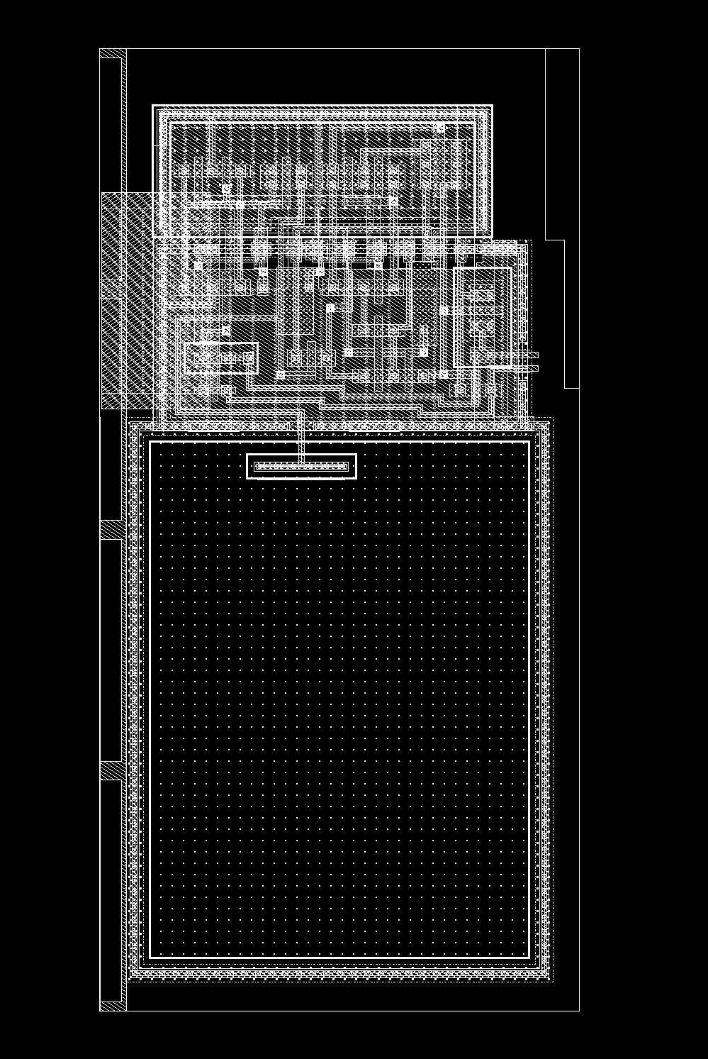
29 Top Layout The NP layout is hierarchically used in a top level design to create an array of processors. Alongside the processor array is a microcontroller to provide control and communication with the array. The final layout is shown in Figure 4.7. A hierarchical view is shown in Figure 4.8.


30 Figure 4.7: Top Layout 23


31 Figure 4.8: Hierarchical Top Layout 24
32 25 Chapter 5 Verification 5.1 DRC ASSURA was used to ensure the design met the technology design rules. Particular attention was placed on the thick-oxide transistors used in the analog portion due to increased spacing requirements for these N-wells and active regions. Large spaces had to be left on the top and sides of the photodiode to ensure that approaching N-wells from standard cells after IP insertion did not violate thick-oxide transistor spacing rules. Recommended rules for high yield were ignored in order to minimize area and create a layout as compact as possible. At the top level a global DRC check was run which consisted of design rule, antenna, and fill checks. Fill was properly handled by Encounter and did not require any intervention. However, multiple design iterations were done to eliminate all the antenna issues. Some of these were visible early in the design flow, such as the need for tie down diodes on the photodiode. Others were discovered after going to fab, where IP insertion created more problems, such as the standard cell stapling done on metal 1.
33 LVS The photodiode, NP, and top level layout designs were compared to their schematic counterparts in Open Access and Verilog. The photodiode s N-well could not be compared to an ideal capacitor, because the extraction utility, ASSURA QRC, did not recognize the N-well to substrate junction as a capacitance. Thus, a modified schematic without photodiode capacitance was used for LVS. The NP and top level layouts were compared against Verilog utilizing blackboxing techniques on standard cells and pads. The layouts for these are proprietary, so they could not be analyzed during LVS. Blackboxing stops LVS from descending into a cell, instead it simply verifies extracted pin connectivity, making sure it is properly connected. This was particularly important for the photodiode, since no Verilog equivalent was created for the comparator and reset circuitry. At the top level, LVS was able to hierarchically analyze the top level Verilog which made reference to the NP Verilog.
34 27 Chapter 6 Area Minimization Techniques 6.1 Custom Logic Cells A majority of chip area is utilized by sequential logic cells in the construction of memory elements and registers throughout the digital design. To help reduce area utilization and provide more area for routing channels and pixel elements, the most heavily utilized cell was redesigned. A report of area utilization is shown in Table 6.1. If we create our own sequential logic cell, we can improve area utilization by providing a less robust, but much smaller digital flip-flop (DFF). The design that Table 6.1: Area Utilization Type Area (µm 2 µm 2 ) Area % timing 3,774, sequential 3,261, inverter 24, buffer 43, clock gating 481, logic 1,275, total 8,861,

35 28 Figure 6.1: C 2 MOS DFF Design was chosen used a clocked gate composed of two tristate buffers in series that could hold a logic state between them using an internal capacitance across net X, shown in Figure 6.1 [5]. This design uses eight fewer transistors than a standard transmission gate design, shown in Figure 6.2.

36 Figure 6.2: Transmission Gate DFF Design 29
37 DFF Layout The final layout of the DFF is shown in Figure 6.3. To maximize routing ability and minimize the number of layers used, active and poly were used as routing layers. The design rules were pushed to the limits and recommended rules were ignored to ensure minimum area utilization. Special logic-only rules were applied to the design to further allow area minimization and allow the smallest possible DFF design. The height is matched to the standard cell library s. In 0.13µm it is not possible to make the design any smaller width-wise. 6.3 Encounter Library Characterizer After a layout and abstract were created for the new DFF, Encounter needed timing and characterization data to be able to recognize its functionality, place it as a standard cell, and ensure timing was met. The Encounter utility used for this was Encounter Library Characterizer (ELC). ELC received a schematic netlist of the design to be modeled along with a handful of initial conditions and operating ranges for the technology and generated a truth table of conditions to attempt to model based on the pins seen. Next, ELC would run a SPECTRE simulation on the design and feed it various inputs to determine its functionality. The output of this is shown below in ELC s function format and Verilog:


38 Figure 6.3: DFF Layout 31
39 32 DFF, ; module DFF(CK,D,Q); input CK,D; output Q; trireg _n1; notif1(q,_n1,ck); notif0(_n1,d,ck); endmodule ELC properly recognized the flip-flop as a register and identified its internals as two inverters with an internal tristate buffer. The timing library created by ELC was fed into Encounter where it was selected during synthesis for placement. When Encounter sees this register as meeting timing requirements while having less required area than the digital library s flip-flop cell, it is selected for placement and its layout is inserted into the floorplan. 6.4 A Gated Clock After the design of the DFF, analog simulations were run to ensure that the state could be preserved in the case of the clock being turned off to the logic cells due to clock gating. In the case of transmission gate DFF design, a feedback loop ensures the state is not lost, even if clock stops. However, the C 2 MOS design solely relied on an internal capacitance held by two transistors gates, which would leak over time. It was determined that the integrity of the DFF s output could not be guaranteed, so

40 33 Figure 6.4: Ripple Counter it would not be used in the final design. To monitor its abilities in integrating with other standard cells, a test structure was built and included in the top level design. In the test structure were two tests: to interface the DFF with inverters to create a ripple counter, and to feed into a NAND gate from the standard cell library. The schematic for the ripple counter is shown in Figure 6.4. The schematic for the NAND test is shown in Figure 6.5. The combined layout is shown in Figure 6.6.

41 Figure 6.5: NAND Test Structure 34

42 Figure 6.6: DFF Test Structure 35
43 36 Chapter 7 Future Work After the chip is returned from fab, it will be tested and insight on optimizing the design will be incorporated in the next revision. This section highlights the forseeable advances for the chip in various aspects from the hardware level. 7.1 Testbed A test PCB will be made to mount and interface the chip with an external lens and FPGA to task image operations and collect readout data. The results of this board will allow us to determine what kind of manipulations can be done from an external level to optimize imaging capabilities. Some expected examples include the adjustment of the ramp signal s starting and ending voltages to integrate pixels for various lighting conditions, controlling dynamic range. Another tweak that could be made is to slow down the clock during capture, to allow the integration time to be lengthened for very dark scenes or if photodiode capacitance is not as small as we had imagined. The imaging quality seen from this board will also give us insight into how to redesign the photodiodes, if pixel pitch needs to be changed or fill increased.
44 37 Lighting anomalies are not expected but may be seen, such as upper layer metal blocking light capture at oblique angles. 7.2 DFF Test Structures The data collected from the test structures of the custom DFF can have drastic impacts on the area utilization of this chip. If no problems are detected for slow clocks, the DFF could become the new candidiate for low drive strength flip-flops in the entire design, replacing the standard cell ones which take up over a third of the area. If the slow clock is problematic, but the DFF interfaces nicely with the standard cells, then clock gating could be removed from the Encounter flow to create a higher power, but high density imager. Lastly, the ultimate goal would be to create an entire area-conscious standard cell library of our own that targets the most common cells in the design which are currently taking up too much space. The test structure s results are vital in determining the value of pursuing a task of this order of magnitude. 7.3 Process Scaling If the design were to be respun under a new technology, digital placement and routing would become significantly easier. A newer technology would not only mean smaller area utilization for standard cells and circuitry, but more layers of metal. Currently, in 0.13µm, we have 8 layers of metal, two of which are being reserved for shielding and one which is used by the standard cell library. This left only three layers for analog routing and two layers for digital routing. Even one more layer would allow us to incorporate an entire plane of routing channels in the design, further compacting and optimizing the layout.
45 38 On the other hand, a smaller technology also means analog circuitry will have to be scaled down. Although the photodiode design would also shrink in size, it would also be at the mercy of small channel length effects and leakage currents. Smaller gate oxide thicknesses would inherently mean more tunneling effects and leakage for the comparator and photodiode. The subthreshold bias transistors may also prove to be problematic if voltages cannot be maintained to draw enough current in the comparator to have acceptable slew-rate. 7.4 Parallel Imagers The ultimate goal of this project is to further expand the parallel nature of the architecture to exploit its capabilities. By arranging multiple cameras together, a multi-chip camera could be produced to do distributed camera operations such as tracking or object recognition. The macro-scale could also introduce capabilities such as wireless communication or sensor networks. The parallel nature of these technologies would heavily utilize the abilities of the parallel architecture.
46 39 Bibliography [1] M. Gottardi and W. Yang. A ccd/cmos image sensor array with integrated a/d conversion. In Circuits and Systems, ISCAS 97., Proceedings of 1997 IEEE International Symposium on, volume 3, pages vol.3, [2] S. Kleinfelder, SukHwan Lim, Xinqiao Liu, and A. El Gamal. A frames/s cmos digital pixel sensor. Solid-State Circuits, IEEE Journal of, 36(12): , [3] Anantha Krishna Nelliparthi. A 2-d processor array for massively parallel image processing, [4] P.O. Pouliquen. A ratioless and biasless static cmos level shifter. In Circuits and Systems (ISCAS), Proceedings of 2010 IEEE International Symposium on, pages , [5] Rabaey, Chandraskan, and Nikolic. Digital Integrated Circuits. Prentice Hall, 2nd edition, [6] F. Serra-Graells, J.M. Margarit, and L. Teres. A self-biased and fpn-compensated digital aps for hybrid cmos imagers. In Circuits and Systems, ISCAS IEEE International Symposium on, pages , 2007.
47 40 [7] Hui Tian, Xinqiao Liu, SukHwan Lim, Stuart Kleinfelder, and Abbas El Gamal. Active pixel sensors fabricated in a standard 0.18-µm cmos technology. In Photonics West 2001-Electronic Imaging, pages International Society for Optics and Photonics, [8] D.X.D. Yang, Boyd Fowler, and A. El Gamal. A 128 times;128 pixel cmos area image sensor with multiplexed pixel level a/d conversion. In Custom Integrated Circuits Conference, 1996., Proceedings of the IEEE 1996, pages , [9] D.X.D. Yang, Boyd Fowler, and A.E. Gamal. A nyquist rate pixel level adc for cmos image sensors. In Custom Integrated Circuits Conference, Proceedings of the IEEE 1998, pages , [10] Hongbo Zhu and T. Shibata. A real-time motion-feature-extraction image processor employing digital-pixel-sensor-based parallel architecture. In Circuits and Systems (ISCAS), 2012 IEEE International Symposium on, pages , 2012.
Active Pixel Sensors Fabricated in a Standard 0.18 um CMOS Technology
 Active Pixel Sensors Fabricated in a Standard.18 um CMOS Technology Hui Tian, Xinqiao Liu, SukHwan Lim, Stuart Kleinfelder, and Abbas El Gamal Information Systems Laboratory, Stanford University Stanford,
Jack Keil Wolf Lecture. ESE 570: Digital Integrated Circuits and VLSI Fundamentals. Lecture Outline. MOSFET N-Type, P-Type.
 ESE 570: Digital Integrated Circuits and VLSI Fundamentals Jack Keil Wolf Lecture Lec 3: January 24, 2019 MOS Fabrication pt. 2: Design Rules and Layout http://www.ese.upenn.edu/about-ese/events/wolf.php
PHYSICAL STRUCTURE OF CMOS INTEGRATED CIRCUITS. Dr. Mohammed M. Farag
 PHYSICAL STRUCTURE OF CMOS INTEGRATED CIRCUITS Dr. Mohammed M. Farag Outline Integrated Circuit Layers MOSFETs CMOS Layers Designing FET Arrays EE 432 VLSI Modeling and Design 2 Integrated Circuit Layers
Fundamentals of CMOS Image Sensors
 CHAPTER 2 Fundamentals of CMOS Image Sensors Mixed-Signal IC Design for Image Sensor 2-1 Outline Photoelectric Effect Photodetectors CMOS Image Sensor(CIS) Array Architecture CIS Peripherals Design Considerations
UNIT-II LOW POWER VLSI DESIGN APPROACHES
 UNIT-II LOW POWER VLSI DESIGN APPROACHES Low power Design through Voltage Scaling: The switching power dissipation in CMOS digital integrated circuits is a strong function of the power supply voltage.
ESE 570: Digital Integrated Circuits and VLSI Fundamentals
 ESE 570: Digital Integrated Circuits and VLSI Fundamentals Lec 3: January 24, 2019 MOS Fabrication pt. 2: Design Rules and Layout Penn ESE 570 Spring 2019 Khanna Jack Keil Wolf Lecture http://www.ese.upenn.edu/about-ese/events/wolf.php
Sticks Diagram & Layout. Part II
 Sticks Diagram & Layout Part II Well and Substrate Taps Substrate must be tied to GND and n-well to V DD Metal to lightly-doped semiconductor forms poor connection called Shottky Diode Use heavily doped
UNIT-III POWER ESTIMATION AND ANALYSIS
 UNIT-III POWER ESTIMATION AND ANALYSIS In VLSI design implementation simulation software operating at various levels of design abstraction. In general simulation at a lower-level design abstraction offers
2009 Spring CS211 Digital Systems & Lab 1 CHAPTER 3: TECHNOLOGY (PART 2)
") 1 CHAPTER 3: IMPLEMENTATION TECHNOLOGY (PART 2) Whatwillwelearninthischapter? we learn in this 2 How transistors operate and form simple switches CMOS logic gates IC technology FPGAs and other PLDs Basic
1 CHAPTER 3: IMPLEMENTATION TECHNOLOGY (PART 2) Whatwillwelearninthischapter? we learn in this 2 How transistors operate and form simple switches CMOS logic gates IC technology FPGAs and other PLDs Basic
High Temperature Mixed Signal Capabilities
 High Temperature Mixed Signal Capabilities June 29, 2017 Product Overview Features o Up to 300 o C Operation o Will support most analog functions. o Easily combined with up to 30K digital gates. o 1.0u
A CMOS Image Sensor with Ultra Wide Dynamic Range Floating-Point Pixel-Level ADC
 A 640 512 CMOS Image Sensor with Ultra Wide Dynamic Range Floating-Point Pixel-Level ADC David X.D. Yang, Abbas El Gamal, Boyd Fowler, and Hui Tian Information Systems Laboratory Electrical Engineering
A Survey of the Low Power Design Techniques at the Circuit Level
 A Survey of the Low Power Design Techniques at the Circuit Level Hari Krishna B Assistant Professor, Department of Electronics and Communication Engineering, Vagdevi Engineering College, Warangal, India
! Review: MOS IV Curves and Switch Model. ! MOS Device Layout. ! Inverter Layout. ! Gate Layout and Stick Diagrams. ! Design Rules. !
 ESE 570: Digital Integrated Circuits and VLSI Fundamentals Lec 3: January 21, 2016 MOS Fabrication pt. 2: Design Rules and Layout Lecture Outline! Review: MOS IV Curves and Switch Model! MOS Device Layout!
ESE 570: Digital Integrated Circuits and VLSI Fundamentals
 ESE 570: Digital Integrated Circuits and VLSI Fundamentals Lec 3: January 21, 2016 MOS Fabrication pt. 2: Design Rules and Layout Penn ESE 570 Spring 2016 Khanna Adapted from GATech ESE3060 Slides Lecture
EE 392B: Course Introduction
 EE 392B Course Introduction About EE392B Goals Topics Schedule Prerequisites Course Overview Digital Imaging System Image Sensor Architectures Nonidealities and Performance Measures Color Imaging Recent
A pix 4-kfps 14-bit Digital-Pixel PbSe-CMOS Uncooled MWIR Imager
 IEEE International Symposium on Circuits & Systems ISCAS 2018 Florence, Italy May 27-30 1/26 A 128 128-pix 4-kfps 14-bit Digital-Pixel PbSe-CMOS Uncooled MWIR Imager R. Figueras 1, J.M. Margarit 1, G.
Disseny físic. Disseny en Standard Cells. Enric Pastor Rosa M. Badia Ramon Canal DM Tardor DM, Tardor
 Disseny físic Disseny en Standard Cells Enric Pastor Rosa M. Badia Ramon Canal DM Tardor 2005 DM, Tardor 2005 1 Design domains (Gajski) Structural Processor, memory ALU, registers Cell Device, gate Transistor
Semiconductor Memory: DRAM and SRAM. Department of Electrical and Computer Engineering, National University of Singapore
 Semiconductor Memory: DRAM and SRAM Outline Introduction Random Access Memory (RAM) DRAM SRAM Non-volatile memory UV EPROM EEPROM Flash memory SONOS memory QD memory Introduction Slow memories Magnetic
Lecture 0: Introduction
 Lecture 0: Introduction Introduction Integrated circuits: many transistors on one chip. Very Large Scale Integration (VLSI): bucketloads! Complementary Metal Oxide Semiconductor Fast, cheap, low power
CHAPTER 6 DIGITAL CIRCUIT DESIGN USING SINGLE ELECTRON TRANSISTOR LOGIC
 94 CHAPTER 6 DIGITAL CIRCUIT DESIGN USING SINGLE ELECTRON TRANSISTOR LOGIC 6.1 INTRODUCTION The semiconductor digital circuits began with the Resistor Diode Logic (RDL) which was smaller in size, faster
444 Index. F Fermi potential, 146 FGMOS transistor, 20 23, 57, 83, 84, 98, 205, 208, 213, 215, 216, 241, 242, 251, 280, 311, 318, 332, 354, 407
 Index A Accuracy active resistor structures, 46, 323, 328, 329, 341, 344, 360 computational circuits, 171 differential amplifiers, 30, 31 exponential circuits, 285, 291, 292 multifunctional structures,
A Self-Contained Large-Scale FPAA Development Platform
 A SelfContained LargeScale FPAA Development Platform Christopher M. Twigg, Paul E. Hasler, Faik Baskaya School of Electrical and Computer Engineering Georgia Institute of Technology, Atlanta, Georgia 303320250
CMOS VLSI IC Design. A decent understanding of all tasks required to design and fabricate a chip takes years of experience
 CMOS VLSI IC Design A decent understanding of all tasks required to design and fabricate a chip takes years of experience 1 Commonly used keywords INTEGRATED CIRCUIT (IC) many transistors on one chip VERY
DIGITAL INTEGRATED CIRCUITS A DESIGN PERSPECTIVE 2 N D E D I T I O N
 DIGITAL INTEGRATED CIRCUITS A DESIGN PERSPECTIVE 2 N D E D I T I O N Jan M. Rabaey, Anantha Chandrakasan, and Borivoje Nikolic CONTENTS PART I: THE FABRICS Chapter 1: Introduction (32 pages) 1.1 A Historical
DESIGN OF MULTIPLYING DELAY LOCKED LOOP FOR DIFFERENT MULTIPLYING FACTORS
 DESIGN OF MULTIPLYING DELAY LOCKED LOOP FOR DIFFERENT MULTIPLYING FACTORS Aman Chaudhary, Md. Imtiyaz Chowdhary, Rajib Kar Department of Electronics and Communication Engg. National Institute of Technology,
An Analog Phase-Locked Loop
 1 An Analog Phase-Locked Loop Greg Flewelling ABSTRACT This report discusses the design, simulation, and layout of an Analog Phase-Locked Loop (APLL). The circuit consists of five major parts: A differential
+1 (479)
") Introduction to VLSI Design http://csce.uark.edu +1 (479) 575-6043 yrpeng@uark.edu Invention of the Transistor Vacuum tubes ruled in first half of 20th century Large, expensive, power-hungry, unreliable
Introduction to VLSI Design http://csce.uark.edu +1 (479) 575-6043 yrpeng@uark.edu Invention of the Transistor Vacuum tubes ruled in first half of 20th century Large, expensive, power-hungry, unreliable
! Review: MOS IV Curves and Switch Model. ! MOS Device Layout. ! Inverter Layout. ! Gate Layout and Stick Diagrams. ! Design Rules. !
 ESE 570: Digital Integrated Circuits and VLSI Fundamentals Lec 3: January 21, 2017 MOS Fabrication pt. 2: Design Rules and Layout Lecture Outline! Review: MOS IV Curves and Switch Model! MOS Device Layout!
Implementation of Pixel Array Bezel-Less Cmos Fingerprint Sensor
 Article DOI: 10.21307/ijssis-2018-013 Issue 0 Vol. 0 Implementation of 144 64 Pixel Array Bezel-Less Cmos Fingerprint Sensor Seungmin Jung School of Information and Technology, Hanshin University, 137
Engr354: Digital Logic Circuits
 Engr354: Digital Logic Circuits Chapter 3: Implementation Technology Curtis Nelson Chapter 3 Overview In this chapter you will learn about: How transistors are used as switches; Integrated circuit technology;
ALPS: An Automatic Layouter for Pass-Transistor Cell Synthesis
 ALPS: An Automatic Layouter for Pass-Transistor Cell Synthesis Yasuhiko Sasaki Central Research Laboratory Hitachi, Ltd. Kokubunji, Tokyo, 185, Japan Kunihito Rikino Hitachi Device Engineering Kokubunji,
Active Pixel Sensors Fabricated in a Standard 0.18 urn CMOS Technology
 Active Pixel Sensors Fabricated in a Standard 0.18 urn CMOS Technology Hui Tian, Xinqiao Liu, SukHwan Lim, Stuart Kleinfelder, and Abbas El Gamal Information Systems Laboratory, Stanford University Stanford,
Very Large Scale Integration (VLSI)
") Very Large Scale Integration (VLSI) Lecture 6 Dr. Ahmed H. Madian Ah_madian@hotmail.com Dr. Ahmed H. Madian-VLSI 1 Contents Array subsystems Gate arrays technology Sea-of-gates Standard cell Macrocell
Very Large Scale Integration (VLSI) Lecture 6 Dr. Ahmed H. Madian Ah_madian@hotmail.com Dr. Ahmed H. Madian-VLSI 1 Contents Array subsystems Gate arrays technology Sea-of-gates Standard cell Macrocell
Low-Power Digital CMOS Design: A Survey
 Low-Power Digital CMOS Design: A Survey Krister Landernäs June 4, 2005 Department of Computer Science and Electronics, Mälardalen University Abstract The aim of this document is to provide the reader with
Semiconductor Detector Systems
 Semiconductor Detector Systems Helmuth Spieler Physics Division, Lawrence Berkeley National Laboratory OXFORD UNIVERSITY PRESS ix CONTENTS 1 Detector systems overview 1 1.1 Sensor 2 1.2 Preamplifier 3
CS302 - Digital Logic Design Glossary By
 CS302 - Digital Logic Design Glossary By ABEL : Advanced Boolean Expression Language; a software compiler language for SPLD programming; a type of hardware description language (HDL) Adder : A digital
30 ma flash LDO voltage regulator (output voltage 1.8 ± 0.2 V)
") SPECIFICATION 1 FEATURES Global Foundries CMOS 55 nm Low drop out Low current consumption Two modes operations: Normal, Economy Mode operation Bypass No discrete filtering capacitors required (cap-less
SPECIFICATION 1 FEATURES Global Foundries CMOS 55 nm Low drop out Low current consumption Two modes operations: Normal, Economy Mode operation Bypass No discrete filtering capacitors required (cap-less
Sony IMX Megapixel, 1.4 µm Pixel 1/3.2 Optical Format CMOS Image Sensor
 Sony IMX046 8.11 Megapixel, 1.4 µm Pixel 1/3.2 Optical Format CMOS Image Sensor Imager Process Review For comments, questions, or more information about this report, or for any additional technical needs
Electronic Circuits EE359A
 Electronic Circuits EE359A Bruce McNair B206 bmcnair@stevens.edu 201-216-5549 1 Memory and Advanced Digital Circuits - 2 Chapter 11 2 Figure 11.1 (a) Basic latch. (b) The latch with the feedback loop opened.
3084 IEEE TRANSACTIONS ON NUCLEAR SCIENCE, VOL. 60, NO. 4, AUGUST 2013
 3084 IEEE TRANSACTIONS ON NUCLEAR SCIENCE, VOL. 60, NO. 4, AUGUST 2013 Dummy Gate-Assisted n-mosfet Layout for a Radiation-Tolerant Integrated Circuit Min Su Lee and Hee Chul Lee Abstract A dummy gate-assisted
Characterization of CMOS Image Sensors with Nyquist Rate Pixel Level ADC
 Characterization of CMOS Image Sensors with Nyquist Rate Pixel Level ADC David Yang, Hui Tian, Boyd Fowler, Xinqiao Liu, and Abbas El Gamal Information Systems Laboratory, Stanford University, Stanford,
Preface to Third Edition Deep Submicron Digital IC Design p. 1 Introduction p. 1 Brief History of IC Industry p. 3 Review of Digital Logic Gate
 Preface to Third Edition p. xiii Deep Submicron Digital IC Design p. 1 Introduction p. 1 Brief History of IC Industry p. 3 Review of Digital Logic Gate Design p. 6 Basic Logic Functions p. 6 Implementation
Low Power, Area Efficient FinFET Circuit Design
 Low Power, Area Efficient FinFET Circuit Design Michael C. Wang, Princeton University Abstract FinFET, which is a double-gate field effect transistor (DGFET), is more versatile than traditional single-gate
Basic Fabrication Steps
 Basic Fabrication Steps and Layout Somayyeh Koohi Department of Computer Engineering Adapted with modifications from lecture notes prepared by author Outline Fabrication steps Transistor structures Transistor
Ruixing Yang
 Design of the Power Switching Network Ruixing Yang 15.01.2009 Outline Power Gating implementation styles Sleep transistor power network synthesis Wakeup in-rush current control Wakeup and sleep latency
Implementation of dual stack technique for reducing leakage and dynamic power
 Implementation of dual stack technique for reducing leakage and dynamic power Citation: Swarna, KSV, Raju Y, David Solomon and S, Prasanna 2014, Implementation of dual stack technique for reducing leakage
Wafer-scale 3D integration of silicon-on-insulator RF amplifiers
 Wafer-scale integration of silicon-on-insulator RF amplifiers The MIT Faculty has made this article openly available. Please share how this access benefits you. Your story matters. Citation As Published
FDTD SPICE Analysis of High-Speed Cells in Silicon Integrated Circuits
 FDTD Analysis of High-Speed Cells in Silicon Integrated Circuits Neven Orhanovic and Norio Matsui Applied Simulation Technology Gateway Place, Suite 8 San Jose, CA 9 {neven, matsui}@apsimtech.com Abstract
Contents 1 Introduction 2 MOS Fabrication Technology
 Contents 1 Introduction... 1 1.1 Introduction... 1 1.2 Historical Background [1]... 2 1.3 Why Low Power? [2]... 7 1.4 Sources of Power Dissipations [3]... 9 1.4.1 Dynamic Power... 10 1.4.2 Static Power...
UMAINE ECE Morse Code ROM and Transmitter at ISM Band Frequency
 UMAINE ECE Morse Code ROM and Transmitter at ISM Band Frequency Jamie E. Reinhold December 15, 2011 Abstract The design, simulation and layout of a UMAINE ECE Morse code Read Only Memory and transmitter
A New Capacitive Sensing Circuit using Modified Charge Transfer Scheme
 78 Hyeopgoo eo : A NEW CAPACITIVE CIRCUIT USING MODIFIED CHARGE TRANSFER SCHEME A New Capacitive Sensing Circuit using Modified Charge Transfer Scheme Hyeopgoo eo, Member, KIMICS Abstract This paper proposes
The Design and Characterization of an 8-bit ADC for 250 o C Operation
 The Design and Characterization of an 8-bit ADC for 25 o C Operation By Lynn Reed, John Hoenig and Vema Reddy Tekmos, Inc. 791 E. Riverside Drive, Bldg. 2, Suite 15, Austin, TX 78744 Abstract Many high
1 FUNDAMENTAL CONCEPTS What is Noise Coupling 1
 Contents 1 FUNDAMENTAL CONCEPTS 1 1.1 What is Noise Coupling 1 1.2 Resistance 3 1.2.1 Resistivity and Resistance 3 1.2.2 Wire Resistance 4 1.2.3 Sheet Resistance 5 1.2.4 Skin Effect 6 1.2.5 Resistance
420 Intro to VLSI Design
 Dept of Electrical and Computer Engineering 420 Intro to VLSI Design Lecture 0: Course Introduction and Overview Valencia M. Joyner Spring 2005 Getting Started Syllabus About the Instructor Labs, Problem
ISSN: [Pandey * et al., 6(9): September, 2017] Impact Factor: 4.116
![ISSN: [Pandey * et al., 6(9): September, 2017] Impact Factor: 4.116](/thumbs/87/96519609.jpg "ISSN: [Pandey * et al., 6(9): September, 2017] Impact Factor: 4.116") IJESRT INTERNATIONAL JOURNAL OF ENGINEERING SCIENCES & RESEARCH TECHNOLOGY A VLSI IMPLEMENTATION FOR HIGH SPEED AND HIGH SENSITIVE FINGERPRINT SENSOR USING CHARGE ACQUISITION PRINCIPLE Kumudlata Bhaskar
IJESRT INTERNATIONAL JOURNAL OF ENGINEERING SCIENCES & RESEARCH TECHNOLOGY A VLSI IMPLEMENTATION FOR HIGH SPEED AND HIGH SENSITIVE FINGERPRINT SENSOR USING CHARGE ACQUISITION PRINCIPLE Kumudlata Bhaskar
Techniques for Pixel Level Analog to Digital Conversion
 Techniques for Level Analog to Digital Conversion Boyd Fowler, David Yang, and Abbas El Gamal Stanford University Aerosense 98 3360-1 1 Approaches to Integrating ADC with Image Sensor Chip Level Image
Lecture Notes 5 CMOS Image Sensor Device and Fabrication
 Lecture Notes 5 CMOS Image Sensor Device and Fabrication CMOS image sensor fabrication technologies Pixel design and layout Imaging performance enhancement techniques Technology scaling, industry trends
AN EFFICIENT APPROACH TO MINIMIZE POWER AND AREA IN CARRY SELECT ADDER USING BINARY TO EXCESS ONE CONVERTER
 AN EFFICIENT APPROACH TO MINIMIZE POWER AND AREA IN CARRY SELECT ADDER USING BINARY TO EXCESS ONE CONVERTER K. RAMAMOORTHY 1 T. CHELLADURAI 2 V. MANIKANDAN 3 1 Department of Electronics and Communication
ECEN689: Special Topics in Optical Interconnects Circuits and Systems Spring 2016
 ECEN689: Special Topics in Optical Interconnects Circuits and Systems Spring 2016 Lecture 10: Electroabsorption Modulator Transmitters Sam Palermo Analog & Mixed-Signal Center Texas A&M University Announcements
Photons and solid state detection
 Photons and solid state detection Photons represent discrete packets ( quanta ) of optical energy Energy is hc/! (h: Planck s constant, c: speed of light,! : wavelength) For solid state detection, photons
Putting It All Together: Computer Architecture and the Digital Camera
 461 Putting It All Together: Computer Architecture and the Digital Camera This book covers many topics in circuit analysis and design, so it is only natural to wonder how they all fit together and how
Investigation on Performance of high speed CMOS Full adder Circuits
 ISSN (O): 2349-7084 International Journal of Computer Engineering In Research Trends Available online at: www.ijcert.org Investigation on Performance of high speed CMOS Full adder Circuits 1 KATTUPALLI
High Voltage Operational Amplifiers in SOI Technology
 High Voltage Operational Amplifiers in SOI Technology Kishore Penmetsa, Kenneth V. Noren, Herbert L. Hess and Kevin M. Buck Department of Electrical Engineering, University of Idaho Abstract This paper
Micron MT9T Megapixel, ¼ Optical Format, 1.75 µm Pixel Size System-on-Chip (SOC) CMOS Image Sensor
 CMOS Image Sensor") Micron MT9T111 3.1 Megapixel, ¼ Optical Format, 1.75 µm Pixel Size System-on-Chip (SOC) CMOS Image Sensor Imager Process Review with Optional TEM Analysis of SRAM For comments, questions, or more information
Micron MT9T111 3.1 Megapixel, ¼ Optical Format, 1.75 µm Pixel Size System-on-Chip (SOC) CMOS Image Sensor Imager Process Review with Optional TEM Analysis of SRAM For comments, questions, or more information
ECE/CoE 0132: FETs and Gates
 ECE/CoE 0132: FETs and Gates Kartik Mohanram September 6, 2017 1 Physical properties of gates Over the next 2 lectures, we will discuss some of the physical characteristics of integrated circuits. We will
CHAPTER 1 INTRODUCTION
 CHAPTER 1 INTRODUCTION 1.1 Historical Background Recent advances in Very Large Scale Integration (VLSI) technologies have made possible the realization of complete systems on a single chip. Since complete
A CMOS Imager with PFM/PWM Based Analogto-digital
 Edith Cowan University Research Online ECU Publications Pre. 2011 2002 A CMOS Imager with PFM/PWM Based Analogto-digital Converter Amine Bermak Edith Cowan University 10.1109/ISCAS.2002.1010386 This conference
Aptina MT9P111 5 Megapixel, 1/4 Inch Optical Format, System-on-Chip (SoC) CMOS Image Sensor
 CMOS Image Sensor") Aptina MT9P111 5 Megapixel, 1/4 Inch Optical Format, System-on-Chip (SoC) CMOS Image Sensor Imager Process Review For comments, questions, or more information about this report, or for any additional technical
Aptina MT9P111 5 Megapixel, 1/4 Inch Optical Format, System-on-Chip (SoC) CMOS Image Sensor Imager Process Review For comments, questions, or more information about this report, or for any additional technical
EE 330 Lecture 44. Digital Circuits. Ring Oscillators Sequential Logic Array Logic Memory Arrays. Final: Tuesday May 2 7:30-9:30
 EE 330 Lecture 44 igital Circuits Ring Oscillators Sequential Logic Array Logic Memory Arrays Final: Tuesday May 2 7:30-9:30 Review from Last Time ynamic Logic Basic ynamic Logic Gate V F A n PN Any of
A Digital Clock Multiplier for Globally Asynchronous Locally Synchronous Designs
 A Digital Clock Multiplier for Globally Asynchronous Locally Synchronous Designs Thomas Olsson, Peter Nilsson, and Mats Torkelson. Dept of Applied Electronics, Lund University. P.O. Box 118, SE-22100,
Imaging serial interface ROM
 Page 1 of 6 ( 3 of 32 ) United States Patent Application 20070024904 Kind Code A1 Baer; Richard L. ; et al. February 1, 2007 Imaging serial interface ROM Abstract Imaging serial interface ROM (ISIROM).
Computer-Based Project on VLSI Design Co 3/8
 Computer-Based Project on VLSI Design Co 3/8 This pamphlet describes a laboratory activity based on a former third year EIST experiment. Its purpose is the measurement of the switching speed of some CMOS
Lecture 12 Memory Circuits. Memory Architecture: Decoders. Semiconductor Memory Classification. Array-Structured Memory Architecture RWM NVRWM ROM
 Semiconductor Memory Classification Lecture 12 Memory Circuits RWM NVRWM ROM Peter Cheung Department of Electrical & Electronic Engineering Imperial College London Reading: Weste Ch 8.3.1-8.3.2, Rabaey
Design of High Gain Two stage Op-Amp using 90nm Technology
 Design of High Gain Two stage Op-Amp using 90nm Technology Shaik Aqeel 1, P. Krishna Deva 2, C. Mahesh Babu 3 and R.Ganesh 4 1 CVR College of Engineering/UG Student, Hyderabad, India 2 CVR College of Engineering/UG
Implementing a 5-bit Folding and Interpolating Analog to Digital Converter
 Implementing a 5-bit Folding and Interpolating Analog to Digital Converter Zachary A Pfeffer (pfefferz@colorado.edu) Department of Electrical and Computer Engineering University of Colorado, Boulder CO
Design of a Folded Cascode Operational Amplifier in a 1.2 Micron Silicon-Carbide CMOS Process
 University of Arkansas, Fayetteville ScholarWorks@UARK Electrical Engineering Undergraduate Honors Theses Electrical Engineering 5-2017 Design of a Folded Cascode Operational Amplifier in a 1.2 Micron
Ultra-high resolution 14,400 pixel trilinear color image sensor
 Ultra-high resolution 14,400 pixel trilinear color image sensor Thomas Carducci, Antonio Ciccarelli, Brent Kecskemety Microelectronics Technology Division Eastman Kodak Company, Rochester, New York 14650-2008
An introduction to Depletion-mode MOSFETs By Linden Harrison
 An introduction to Depletion-mode MOSFETs By Linden Harrison Since the mid-nineteen seventies the enhancement-mode MOSFET has been the subject of almost continuous global research, development, and refinement
POWER GATING. Power-gating parameters
 POWER GATING Power Gating is effective for reducing leakage power [3]. Power gating is the technique wherein circuit blocks that are not in use are temporarily turned off to reduce the overall leakage
Image sensor combining the best of different worlds
 Image sensors and vision systems Image sensor combining the best of different worlds First multispectral time-delay-and-integration (TDI) image sensor based on CCD-in-CMOS technology. Introduction Jonathan
Computer-Based Project on VLSI Design Co 3/7
 Computer-Based Project on VLSI Design Co 3/7 Electrical Characterisation of CMOS Ring Oscillator This pamphlet describes a laboratory activity based on an integrated circuit originally designed and tested
A design of 16-bit adiabatic Microprocessor core
 194 A design of 16-bit adiabatic Microprocessor core Youngjoon Shin, Hanseung Lee, Yong Moon, and Chanho Lee Abstract A 16-bit adiabatic low-power Microprocessor core is designed. The processor consists
DESIGN OF A NOVEL CURRENT MIRROR BASED DIFFERENTIAL AMPLIFIER DESIGN WITH LATCH NETWORK. Thota Keerthi* 1, Ch. Anil Kumar 2
 ISSN 2277-2685 IJESR/October 2014/ Vol-4/Issue-10/682-687 Thota Keerthi et al./ International Journal of Engineering & Science Research DESIGN OF A NOVEL CURRENT MIRROR BASED DIFFERENTIAL AMPLIFIER DESIGN
due to power supply and technology. Process specifications were obtained from the MOSIS
 design number 85739 VLSI Design Chromatic Instrument Tuner For the design of the operational amplifier, we have to take into consideration the constraints due to power supply and technology. Process specifications
Sony. IMX135 Exmor RS 13 Mp Stacked CMOS Image Sensor. Circuit Analysis of Row Control, Column Data Readout and Control, and Ramp Generator
 Sony IMX135 Exmor RS 13 Mp Stacked CMOS Image Sensor Circuit Analysis of Row Control, Column Data Readout and Control, and Ramp Generator 1891 Robertson Road, Suite 500, Ottawa, ON K2H 5B7 Canada Tel:
Yet, many signal processing systems require both digital and analog circuits. To enable
 Introduction Field-Programmable Gate Arrays (FPGAs) have been a superb solution for rapid and reliable prototyping of digital logic systems at low cost for more than twenty years. Yet, many signal processing
NanoFabrics: : Spatial Computing Using Molecular Electronics
 NanoFabrics: : Spatial Computing Using Molecular Electronics Seth Copen Goldstein and Mihai Budiu Computer Architecture, 2001. Proceedings. 28th Annual International Symposium on 30 June-4 4 July 2001
A 1.3 Megapixel CMOS Imager Designed for Digital Still Cameras
 A 1.3 Megapixel CMOS Imager Designed for Digital Still Cameras Paul Gallagher, Andy Brewster VLSI Vision Ltd. San Jose, CA/USA Abstract VLSI Vision Ltd. has developed the VV6801 color sensor to address
Samsung S5K3L1YX Mp, 1/3.2 Inch Optical Format 1.12 µm Pixel Pitch Back Illuminated (BSI) CMOS Image Sensor
 CMOS Image Sensor") Samsung S5K3L1YX03 12.1 Mp, 1/3.2 Inch Optical Format 1.12 µm Pixel Pitch Back Illuminated (BSI) CMOS Image Sensor Circuit Analysis of Pixel Array, Row Drivers, Column Readouts, Ramp Generator, DPLL, MIPI
Samsung S5K3L1YX03 12.1 Mp, 1/3.2 Inch Optical Format 1.12 µm Pixel Pitch Back Illuminated (BSI) CMOS Image Sensor Circuit Analysis of Pixel Array, Row Drivers, Column Readouts, Ramp Generator, DPLL, MIPI
CMOS Digital Logic Design with Verilog. Chapter1 Digital IC Design &Technology
 CMOS Digital Logic Design with Verilog Chapter1 Digital IC Design &Technology Chapter Overview: In this chapter we study the concept of digital hardware design & technology. This chapter deals the standard
! MOS Device Layout. ! Inverter Layout. ! Gate Layout and Stick Diagrams. ! Design Rules. ! Standard Cells. ! CMOS Process Enhancements
 EE 570: igital Integrated Circuits and VLI Fundamentals Lec 3: January 18, 2018 MO Fabrication pt. 2: esign Rules and Layout Lecture Outline! MO evice Layout! Inverter Layout! Gate Layout and tick iagrams!
White Paper Stratix III Programmable Power
 Introduction White Paper Stratix III Programmable Power Traditionally, digital logic has not consumed significant static power, but this has changed with very small process nodes. Leakage current in digital
Fixing Antenna Problem by Dynamic Diode Dropping and Jumper Insertion
 Fixing Antenna Problem by Dynamic Dropping and Jumper Insertion Peter H. Chen and Sunil Malkani Chun-Mou Peng James Lin TeraLogic, Inc. International Tech. Univ. National Semi. Corp. 1240 Villa Street
320MHz Digital Phase Lock Loop. Patrick Spinney Department of Electrical Engineering University of Maine
 320MHz Digital Phase Lock Loop Patrick Spinney Department of Electrical Engineering University of Maine December 2004 Abstract DPLLs (Digital Phase Locked Loop) are commonly used in communications systems.
14.2 Photodiodes 411
 14.2 Photodiodes 411 Maximum reverse voltage is specified for Ge and Si photodiodes and photoconductive cells. Exceeding this voltage can cause the breakdown and severe deterioration of the sensor s performance.
Sony IMX145 8 Mp, 1.4 µm Pixel Pitch Back Illuminated (BSI) CMOS Image Sensor from the Apple iphone 4S Smartphone
 CMOS Image Sensor from the Apple iphone 4S Smartphone") Sony IMX145 8 Mp, 1.4 µm Pixel Pitch Back Illuminated (BSI) CMOS Image Sensor from the Apple iphone 4S Smartphone Imager Process Review 3685 Richmond Road, Suite 500, Ottawa, ON K2H 5B7 Canada Tel: 613-829-0414
Sony IMX145 8 Mp, 1.4 µm Pixel Pitch Back Illuminated (BSI) CMOS Image Sensor from the Apple iphone 4S Smartphone Imager Process Review 3685 Richmond Road, Suite 500, Ottawa, ON K2H 5B7 Canada Tel: 613-829-0414
Sony IMX018 CMOS Image Sensor Imager Process Review
 September 6, 2006 Sony IMX018 CMOS Image Sensor Imager Process Review For comments, questions, or more information about this report, or for any additional technical needs concerning semiconductor technology,
CMOS Schmitt Trigger A Uniquely Versatile Design Component
 CMOS Schmitt Trigger A Uniquely Versatile Design Component INTRODUCTION The Schmitt trigger has found many applications in numerous circuits, both analog and digital. The versatility of a TTL Schmitt is
CMOS Digital Integrated Circuits Analysis and Design
 CMOS Digital Integrated Circuits Analysis and Design Chapter 8 Sequential MOS Logic Circuits 1 Introduction Combinational logic circuit Lack the capability of storing any previous events Non-regenerative
ECE1352. Term Paper Low Voltage Phase-Locked Loop Design Technique
 ECE1352 Term Paper Low Voltage Phase-Locked Loop Design Technique Name: Eric Hu Student Number: 982123400 Date: Nov. 14, 2002 Table of Contents Abstract pg. 04 Chapter 1 Introduction.. pg. 04 Chapter 2