Consumer Electronics: from chip to system
|
|
|
- Leona Smith
- 5 years ago
- Views:
Transcription


1 Consumer Electronics: from chip to system Kees Revenberg Co-founder/MD June 6 th 2018 APC, University of Warwick, UK NMI Techworks
2 CONTENT Introduction Consumer Electronics Definition Trends and concequences Chip manufacturing & Test flow Manufacturing flow Chip specific test procedures and standards System manufacturing & Test flow Manufacturing flow System specific test procedures and standards Interaction between Chip and System functions Failure Analysis from system to chip Summary 2
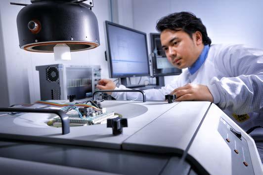
3 INTRODUCTION MASER Engineering is an Independent Service Provider, founded in 1993 and privately held by Hans Kemper and Kees Revenberg 25 years experience in test and analysis of semiconductors, electronic components and electronic systems 2,900 m² office & laboratory at Capitool 56, Enschede, The Netherlands Staff 49 employees (42 FTE), half with PhD/MSc/BSc degree Quality system certification and Accreditation ISO-9001:2008 certification by Lloyds ISO-17025:2005 accreditation according to scope L388 Customer project communication (CMIDS) MIDS internal track and trace system Secure customer interface for project tracking Download function for large result files and images (cmids.maser.nl) 3

4 INTRODUCTION Failure Analysis Non Destructive Analysis Fault Localization Sample Preparation Imaging and Analysis First Silicon Circuit Edit Reliability Test ESD/LU Test Accelerated Life Test Climate and Corrosion Test Temperature Cycling and Shock Mechanical Vibration and Shock 4
5 Consumer Electronics Definition by Wikipedia Consumer electronics or home electronics are equipment intended for everyday use, typically in private homes. Consumer electronics include devices used for entertainment (flat screen TVs, DVD players, video games, remote control cars, etc.), communications (telephones, cell phones, -capable laptops, etc.) and home-office activities (e.g., desktop computers, printers, paper shredders, etc.) Trends and consequences Smart home, outdoor sports and personal medical devices Mobility becomes an electronic gadget with wheels or propeller Long list of topics at the 2019 Consumer Electronics Show in Las Vegas Consumer Electronics Market to hit $1,500bn by 2024: GMI, Inc. 5
6 Consumer Electronics Advertising, Entertainment & Content Gaming Marketing & Advertising Music Virtual Reality & Augmented Reality Automotive Self-Driving Cars Vehicle Technology Health & Wellness Accessibility Digital Health Fitness & Wearables Sleep Technology Sports esports Sports Technology Home & Family Home Entertainment Family & Lifestyle Smart Home Internet of Things (IoT) Smart Cities Product Design & Manufacturing 3D Printing Design, Sourcing & Packaging Sustainability Robotics & Machine Intelligence Artificial Intelligence Drones Robotics Topics CES Las Vegas
7 CE IC design and manufacturing IC design with DFT circuits included and partial simulation Embedded software and Test program development First silicon debug and prototype assembly IC release Qualification lot manufacturing IC qualification Production release IC endurance and monitoring Due to high quantities of CE applications, yield is important The device technology is at edge, both chip and package Application environment and expected life is getting more complex CE IC s are exposed to more stringent test procedures 7

8 Chip Manufacturing & Test flow Manufacturing flow Nowadays >400 steps Semi nodes >7nm Metal layers >10 Complex WL packaging Process monitoring Materials & Chemicals Automatic Inspection In-line Xsie and TEM Monitoring circuit test Wafer test Assembly Singulation and packaging WL packaging and stacking Final product test 8

9 Chip Qualification programs Chip specific test procedures and standards Automotive industry AEC- Q100 to AEC-Q200 Industry standardization organizations like JEDEC JEDEC-47 Application specific and Customer specific ESA-SCC or MIL-STD 883 ESDA + JEDEC 9

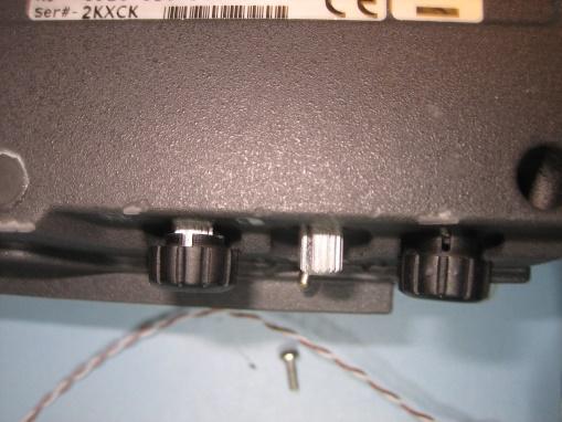
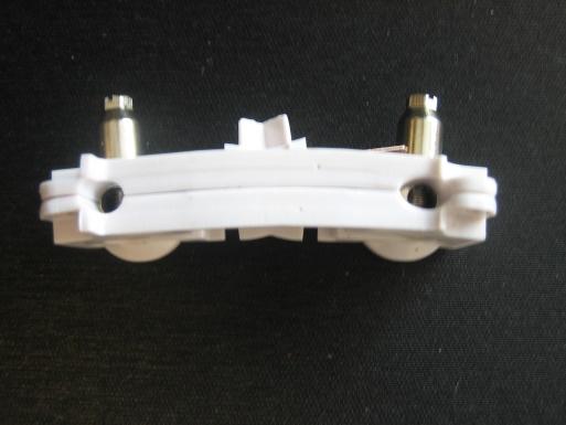
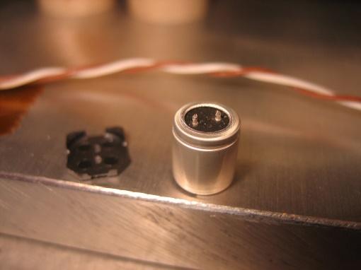
10 CE chip life test setup High end CE application processors high pin count + high power Dynamic Vector driver based on ATE program conversion Individual temperature control by socket heating/cooling Individual function monitoring including PS currents 10
11 CE system design and manufacturing System design with application mission study and FME(C)A Embedded software and Test program development First prototype assembly HALT design evaluation Qualification lot manufacturing system qualification Safety tests and legislation release (CE marking) Production release endurance and HASS monitoring Due to high quantities of CE applications, yield is important Application environment and expected life is getting more complex CE systems are exposed to more stringent test procedures 11
12 HALT: Product Margins definition Lower Destruct Limit Lower Operating Limit Product Specs Upper Operating Limit Upper Destruct Limit Operating Margin Destruct Margin Operating Margin Destruct Margin Stress NMI Techworks
13 HALT: Product Margin Aging Lower Destruct Limit Lower Operating Limit Product Specs Upper Operating Limit Upper Destruct Limit Stress NMI Techworks
14 HALT: process overview Temperature ( C) Vibration (Grms) Time (minutes) 0 Temperature Vibration NMI Techworks
15 HALT essential: Preparation meeting HALT can only be successful after proper preparation At what stage of design process HALT to be performed Preparation meeting with Design, Test and HALT engineer System description Sample size definition, based on cost and availability Functional and Parametric E-test definition Mechanical / Thermal construction assessment Mechanical fixture design directive Parts list scan for destruct limits Initial HALT limits estimation Spare parts and repair guideline Onsite and Standby crew definition during HALT sequence testing HALT planning and quotation NMI Techworks


16 HALT: systems under stress Multiple small units for redundant behavior study Larger systems in partly open position NMI Techworks

17 HALT DEFECT EXAMPLES Electrical detectable Visual detectable Hardware and Embedded Software NMI Techworks


18 Interaction between Chip & System Rapid growth in handheld / portable CE Systems Consumers do drop them or misuse them RMA procedures do not get all defects returned for review Interconnection issues due to dense assembly and lead-free solder EXAMPLE Board Level Reliability Test for Consumers that drop their Electronics 18
19 FAILURE ANALYSIS Failure Analysis flow in the electronics industry Non Destructive Analysis E-test OPTICAL 2D/3D XRAY SAM LIT - EOTPR Fault localization Sample preparation Microscopic Imaging Material Analysis EMMI OBIRCH Thermograph Laser NIR I/V Probing Volt contrast EBIC/EBAC Nano-probing Contact AFM other Laser decap Chemical decap Plasma decap Mechanical Xsie Planar polish Plasma etching FIB Slice+View TEM lamella other Stereo Optical HP Optical Interferometer W-SEM FEG-SEM FEG-sTEM Dual Beam Ion Beam other SEM/EDX stem/edx FTIR Chemical SIMS XPS/ETCA Scanning Auger µ XRF XRD other Report 19


20 CE IC & system test tool examples 20
21 SUMMARY Consumer Electronics is a major part of the electronics market Fast development cycles, high-end technology and large volume High yield is essential in both IC and system level production Preventive test method on IC level DFT and system level HALT More system aspects enter the System in Package IC world CE applications are still a strong growing potential Thank you for your attention! and keep consuming electronics Contact NL: kees.revenberg@maser.nl T: Contact UK: john.watkins@redcroftuk.com T:
STM RH-ASIC capability
 STM RH-ASIC capability JAXA 24 th MicroElectronic Workshop 13 th 14 th October 2011 Prepared by STM Crolles and AeroSpace Unit Deep Sub Micron (DSM) is strategic for Europe Strategic importance of European
Robustness Validation / Mission Profile Compared to AEC-Q100 Standard Qualification Flow
 Robustness Validation / Mission Profile Compared to AEC-Q100 Standard Qualification Flow Jürgen Gruber Zwolle Nördlingen Stuttgart Dresden Bath Outline History of AEC-Q100 qualification procedure Why robustness
microelectronics services high-tech requires high-precision microelectronics services
 ELECTRICAL & ELECTRONICS microelectronics services high-tech requires high-precision microelectronics services WORLDWIDE Analysis, TESTING & CERTIFICATION LOCALLY AVAILABLE worldwide Electrical and electronic
FRAUNHOFER INSTITUTE FOR PHOTONIC MICROSYSTEMS IPMS. Application Area. Quality of Life
 FRAUNHOFER INSTITUTE FOR PHOTONIC MICROSYSTEMS IPMS Application Area Quality of Life Overlay image of visible spectral range (VIS) and thermal infrared range (LWIR). Quality of Life With extensive experience
Special JIGS SPECIAL JIGS FOR CABLE TEST HEAVY DUTY JIGS ESD JIGS JIGS FOR TV-DVD-AUDIO STEERING WHEEL JIGS. Executive test solutions
 Special JIGS Executive test solutions For applications such as testing the connectors on car motors, the Special JIG Design & Engineering Department from Equip-Test can offer you the right solution. SPECIAL
Issue 112 October 2018
 Latch-Up Overview Part 2 By Christopher Henderson In this section, we will continue to discuss the topic of latchup. We will discuss latch-up testing. We perform latch-up testing to determine the robustness
Core Business: Semiconductor-related Inspection Equipment
 Core Business: Semiconductor-related Inspection Equipment Lasertec manufactures unique inspection and measurement systems that incorporate the cutting-edge technologies of applied optics and offers them
Ion Beam Lithography next generation nanofabrication
 Ion Beam Lithography next generation nanofabrication EFUG Bordeaux 2011 ion beams develop Lloyd Peto IBL sales manager Copyright 2011 by Raith GmbH ionline new capabilities You can now Apply an ion beam
Technology Trends for Government
 Technology Trends for Government Leaders @RajneshSingh rds@jugad.in Where we came from Module 4: ICT Trends for Government Leaders First edition: 2007/8 Revised: 2011 But ICT Trends are fast-evolving K
CERTIFICATE OF ACCREDITATION
 CERTIFICATE OF ACCREDITATION ANSI-ASQ National Accreditation Board/ACLASS 500 Montgomery Street, Suite 625, Alexandria, VA 22314, 877-344-3044 This is to certify that Evans Analytical Group, LLC 15 Morgan
ASCENT Overview. European Nanoelectronics Infrastructure Access. MOS-AK Workshop, Infineon, Munich, 13 th March 2018.
 ASCENT Overview MOS-AK Workshop, Infineon, Munich, 13 th March 2018 European Nanoelectronics Infrastructure Access Paul Roseingrave The Challenge Cost/performance returns by scaling are diminishing Cost
Opto-Mechanical Equipment of KBTEM: Present Day and the Future
 KBTEM JSC, Minsk, Belarus Opto-Mechanical Equipment of KBTEM: Present Day and the Future Quality Management System Certificate ISO-9001 since 2001 SPIE Member since 2003 www.kb-omo.by Dr. S.Avakaw SEMI
Packaging Fault Isolation Using Lock-in Thermography
 Packaging Fault Isolation Using Lock-in Thermography Edmund Wright 1, Tony DiBiase 2, Ted Lundquist 2, and Lawrence Wagner 3 1 Intersil Corporation; 2 DCG Systems, Inc.; 3 LWSN Consulting, Inc. Addressing
BEng (Hons) Mechanical
 Mechanical") FACULTY OF ENGINEERING AND TECHNOLOGY (FET) BEng (Hons) Mechanical 1 Programme Information www.mmu.edu.my A four-year course. Started in the year 2000, and was accredited for the first time in November
FACULTY OF ENGINEERING AND TECHNOLOGY (FET) BEng (Hons) Mechanical 1 Programme Information www.mmu.edu.my A four-year course. Started in the year 2000, and was accredited for the first time in November
A Perspective on Semiconductor Equipment. R. B. Herring March 4, 2004
 A Perspective on Semiconductor Equipment R. B. Herring March 4, 2004 Outline Semiconductor Industry Overview of circuit fabrication Semiconductor Equipment Industry Some equipment business strategies Product
Component Package Decapsulation Process with Analogue Signature Analysis Support
 Component Package Decapsulation Process with Analogue Signature Analysis Support NEUMANN PETR, ADAMEK MILAN, SKOCIK PETR Faculty of Applied Informatics Tomas Bata University in Zlin nam.t.g.masaryka 5555
MAPPER: High throughput Maskless Lithography
 MAPPER: High throughput Maskless Lithography Marco Wieland CEA- Leti Alterative Lithography workshop 1 Today s agenda Introduction Applications Qualification of on-tool metrology by in-resist metrology
flexible lighting technology
 As a provider of lighting solutions for the Machine Vision Industry, we are passionate about exceeding our customers expectations. As such, our ISO 9001 quality procedures are at the core of everything
Accelerating Collective Innovation: Investing in the Innovation Landscape
 PCB Executive Forum Accelerating Collective Innovation: Investing in the Innovation Landscape How a Major Player Uses Internal Venture Program to Accelerate Small Players with Big Ideas Dr. Joan K. Vrtis
The Advantages of Integrated MEMS to Enable the Internet of Moving Things
 The Advantages of Integrated MEMS to Enable the Internet of Moving Things January 2018 The availability of contextual information regarding motion is transforming several consumer device applications.
TECHsummit & GadgetExpo Bratislava
 TECHsummit & GadgetExpo Bratislava Hotel Bratislava Date: 11./12.5.2016 Organizers Media Partners Partner Startup Panel Partner B2B Matching Partner Mobility Partner Networking Partner Conference Program
Chapter 2 Mechatronics Disrupted
 Chapter 2 Mechatronics Disrupted Maarten Steinbuch 2.1 How It Started The field of mechatronics started in the 1970s when mechanical systems needed more accurate controlled motions. This forced both industry
Scientific Highlights 2016
 Scientific Highlights 2016 Science and Technology Sector Schools and Faculties Faculty of Science Louvain School of Engineering (EPL) Faculty of Architecture, Architectural Engineering and Urban Planning
Facing Moore s Law with Model-Driven R&D
 Facing Moore s Law with Model-Driven R&D Markus Matthes Executive Vice President Development and Engineering, ASML Eindhoven, June 11 th, 2015 Slide 2 Contents Introducing ASML Lithography, the driving
Energy beam processing and the drive for ultra precision manufacturing
 Energy beam processing and the drive for ultra precision manufacturing An Exploration of Future Manufacturing Technologies in Response to the Increasing Demands and Complexity of Next Generation Smart
Software Computer Vision - Driver Assistance
 Software Computer Vision - Driver Assistance Work @Bosch for developing desktop, web or embedded software and algorithms / computer vision / artificial intelligence for Driver Assistance Systems and Automated
Mask Technology Development in Extreme-Ultraviolet Lithography
 Mask Technology Development in Extreme-Ultraviolet Lithography Anthony Yen September 6, 2013 Projected End of Optical Lithography 2013 TSMC, Ltd 1976 1979 1982 1985 1988 1991 1994 1997 2000 2003 2007 2012
Fabricating 2.5D, 3D, 5.5D Devices
 Fabricating 2.5D, 3D, 5.5D Devices Bob Patti, CTO rpatti@tezzaron.com Tezzar on Semiconduct or 04/15/2013 1 Gen4 Dis-Integrated 3D Memory DRAM layers 42nm node 2 million vertical connections per lay per
Hermetic Packaging Solutions using Borosilicate Glass Thin Films. Lithoglas Hermetic Packaging Solutions using Borosilicate Glass Thin Films
 Hermetic Packaging Solutions using Borosilicate Glass Thin Films 1 Company Profile Company founded in 2006 ISO 9001:2008 qualified since 2011 Headquarters and Production in Dresden, Germany Production
Ultra-thin Die Characterization for Stack-die Packaging
 Ultra-thin Die Characterization for Stack-die Packaging Wei Sun, W.H. Zhu, F.X. Che, C.K. Wang, Anthony Y.S. Sun and H.B. Tan United Test & Assembly Center Ltd (UTAC) Packaging Analysis & Design Center
WHITE PAPER CIRCUIT LEVEL AGING SIMULATIONS PREDICT THE LONG-TERM BEHAVIOR OF ICS
 WHITE PAPER CIRCUIT LEVEL AGING SIMULATIONS PREDICT THE LONG-TERM BEHAVIOR OF ICS HOW TO MINIMIZE DESIGN MARGINS WITH ACCURATE ADVANCED TRANSISTOR DEGRADATION MODELS Reliability is a major criterion for
Market and technology trends in advanced packaging
 Close Market and technology trends in advanced packaging Executive OVERVIEW Recent advances in device miniaturization trends have placed stringent requirements for all aspects of product manufacturing.
Introduction of New Products
 Field Emission Electron Microscope JEM-3100F For evaluation of materials in the fields of nanoscience and nanomaterials science, TEM is required to provide resolution and analytical capabilities that can
Scanning Electron Microscopy
 Scanning Electron Microscopy For the semiconductor industry A tutorial Titel Vorname Nachname Titel Jobtitle, Bereich/Abteilung Overview Scanning Electron microscopy Scanning Electron Microscopy (SEM)
Evolution of Software-Only-Simulation at NASA IV&V
 Evolution of Software-Only-Simulation at NASA IV&V http://www.nasa.gov/centers/ivv/jstar/itc.html Justin McCarty Justin.McCarty@TMCTechnologies.com Justin Morris Justin.R.Morris@Nasa.gov Scott Zemerick
Challenges of EUV masks and preliminary evaluation
 Challenges of EUV masks and preliminary evaluation Naoya Hayashi Electronic Device Laboratory Dai Nippon Printing Co.,Ltd. EUV Mask Workshop 2004 1 Contents Recent Lithography Options on Roadmap Challenges
SEM Magnification Calibration & Verification: Building Confidence in Your Scale Bar
 SEM Magnification Calibration & Verification: Building Confidence in Your Scale Bar Mark A. Koten, Ph.D. Senior Research Scientist Electron Optics Group McCrone Associates Why check your SEM image calibration?
Capabilities of Flip Chip Defects Inspection Method by Using Laser Techniques
 Capabilities of Flip Chip Defects Inspection Method by Using Laser Techniques Sheng Liu and I. Charles Ume* School of Mechanical Engineering Georgia Institute of Technology Atlanta, Georgia 3332 (44) 894-7411(P)
Making a Difference in 2017 IPOs & CES
 SHAREHOLDER UPDATE JANUARY 2017 Making a Difference in 2017 IPOs & CES By Tom Astle IPOs - Will 2017 finally be the year? Our portfolio strategy of investing in later-stage growth companies was partially
Testing Digital Systems II
 Lecture : Introduction Instructor: M. Tahoori Copyright 206, M. Tahoori TDS II: Lecture Today s Lecture Logistics Course Outline Review from TDS I Copyright 206, M. Tahoori TDS II: Lecture 2 Lecture Logistics
Length section: New calibration and research services
 Length section: New calibration and research services O Kruger October 2015 T026 Overview Traditional traceability chart Traceability chart with length R&D projects Overview of Various R&D projects Conclusion
INSPECTION AND REVIEW PORTFOLIO FOR 3D FUTURE
 INSPECTION AND REVIEW PORTFOLIO FOR 3D FUTURE This week announced updates to four systems the 2920 Series, Puma 9850, Surfscan SP5 and edr-7110 intended for defect inspection and review of 16/14nm node
sensors & systems Imagine future imaging... Leti, technology research institute Contact:
 Imaging sensors & systems Imagine future imaging... Leti, technology research institute Contact: leti.contact@cea.fr From consumer markets to high-end applications smart home IR array for human activity
Microwave and Microelectronics
 Microwave and Microelectronics MISSION SYSTEMS 2 BAE Systems Mission Systems Microwave and Microelectronics 3 Manufacturing Success Microwave and Microelectronics Mission Systems provides manufacturing
CSM High-Voltage Measurement Systems
 CSM High-Voltage Measurement Systems Safe Measurement on High-Voltage Components CSM HV Modules // High-Voltage Safe Measurement Systems Safe Measurement on High-Voltage Components E-mobility: enhancing
Lecture 16: Design for Testability. MAH, AEN EE271 Lecture 16 1
 Lecture 16: Testing, Design for Testability MAH, AEN EE271 Lecture 16 1 Overview Reading W&E 7.1-7.3 - Testing Introduction Up to this place in the class we have spent all of time trying to figure out
Plan Optik AG. Plan Optik AG PRODUCT CATALOGUE
 Plan Optik AG Plan Optik AG PRODUCT CATALOGUE 2 In order to service the high demand of wafers more quickly, Plan Optik provides off the shelf products in sizes from 2 up to 300mm diameter. Therefore Plan
Copyright 2000 Society of Photo Instrumentation Engineers.
 Copyright 2000 Society of Photo Instrumentation Engineers. This paper was published in SPIE Proceedings, Volume 4043 and is made available as an electronic reprint with permission of SPIE. One print or
Infineon at a glance
 Infineon at a glance 2017 www.infineon.com We make life easier, safer and greener with technology that achieves more, consumes less and is accessible to everyone. Microelectronics from Infineon is the
Evaluation of high power laser diodes for space applications: effects of the gaseous environment
 Evaluation of high power laser diodes for space applications: effects of the gaseous environment Jorge Piris, E. M. Murphy, B. Sarti European Space Agency, Optoelectronics section, ESTEC. M. Levi, G. Klumel,
Electronic Costing & Technology Experts
 Electronic Costing & Technology Experts 21 rue la Nouë Bras de Fer 44200 Nantes France Phone : +33 (0) 240 180 916 email : info@systemplus.fr www.systemplus.fr March 2016 - Version 1 - written by Romain
SEMI Connects: An Overview of SEMI Worldwide. Theresia Fasinski - Manager Membership Relations, SEMI Europe
 SEMI Connects: An Overview of SEMI Worldwide Theresia Fasinski - Manager Membership Relations, SEMI Europe SEMI Connects to Advance a Global Industry Mission SEMI provides industry stewardship and engages
Diverse Lasers Support Key Microelectronic Packaging Tasks
 Diverse Lasers Support Key Microelectronic Packaging Tasks Written by D Muller, R Patzel, G Oulundsen, H Halou, E Rea 23 July 2018 To support more sophisticated and compact tablets, phones, watches and
Lecture 2: Embedded Systems: An Introduction
 Design & Co-design of Embedded Systems Lecture 2: Embedded Systems: An Introduction Adapted from ECE456 course notes, University of California (Riverside), and EE412 course notes, Princeton University
Benefits. Applications. Pinout. Pin1. SiTime Corporation 990 Almanor Avenue, Suite 200 Sunnyvale, CA (408)
") 1 to 125 MHz Programmable Oscillator Features ±60 ps Peak-Peak Period Jitter Wide frequency range 1 MHz to 125 MHz Low frequency tolerance ±50 ppm or ±100 ppm Operating voltage 1.8V or 2.5 or 3.3 V 2.25V
1 to 125 MHz Programmable Oscillator Features ±60 ps Peak-Peak Period Jitter Wide frequency range 1 MHz to 125 MHz Low frequency tolerance ±50 ppm or ±100 ppm Operating voltage 1.8V or 2.5 or 3.3 V 2.25V
Brief Introduction of Sigurd IC package Assembly
 Brief Introduction of Sigurd IC package Assembly Content Package Development Trend Product Brief Sawing type QFN Representative MEMS Product LGA Light Sensor Proximity Sensor High Yield Capability Low
PicoMaster 100. Unprecedented finesse in creating 3D micro structures. UV direct laser writer for maskless lithography
 UV direct laser writer for maskless lithography Unprecedented finesse in creating 3D micro structures Highest resolution in the market utilizing a 405 nm diode laser Structures as small as 300 nm 375 nm
CREST Cluster Focus & Projects. 23rd February 2015
 CREST Cluster Focus & Projects 23rd February 2015 Domain Areas Clusters focus 1. Optoelectronics/LED and Solid State Lighting 2. Embedded System & Internet of Things 3. IC Design, Test & Validation 4.
Christian Boit TUB Berlin University of Technology Sect. Semiconductor Devices. 1
 Semiconductor Device & Analysis Center Berlin University of Technology Christian Boit TUB Berlin University of Technology Sect. Semiconductor Devices Christian.Boit@TU-Berlin.DE 1 Semiconductor Device
Transistor was first invented by William.B.Shockley, Walter Brattain and John Bardeen of Bell Labratories. In 1961, first IC was introduced.
 Unit 1 Basic MOS Technology Transistor was first invented by William.B.Shockley, Walter Brattain and John Bardeen of Bell Labratories. In 1961, first IC was introduced. Levels of Integration:- i) SSI:-
Future challenges in high-frequency electromagnetic metrology (RF to terahertz)
") Prof Nick Ridler IEEE Fellow Electromagnetics Science Leader National Physical Laboratory, UK CCEM workshop Future challenges in electrical metrology, BIPM, Paris, 23 March 2017 Focus on three new measurement
Prof Nick Ridler IEEE Fellow Electromagnetics Science Leader National Physical Laboratory, UK CCEM workshop Future challenges in electrical metrology, BIPM, Paris, 23 March 2017 Focus on three new measurement
The 3D Silicon Leader
 The 3D Silicon Leader 3D Silicon IPD for smaller and more reliable Implantable Medical Devices ATW on Advanced Packaging for Wireless Medical Devices Mohamed Mehdi Jatlaoui, Sébastien Leruez, Olivier Gaborieau,
COMPUTER SCIENCE AND ENGINEERING
 COMPUTER SCIENCE AND ENGINEERING Internet of Thing Cloud Computing Big Data Analytics Network Security Distributed System Image Processing Data Science Business Intelligence Wireless Sensor Network Artificial
IGBT Module Manufacturing & Failure Analysis Process. Seon Kenny (IFKOR QM IPC) Sep
 Sep") IGBT Module Manufacturing & Failure Analysis Process Seon Kenny (IFKOR QM IPC) Sep-11-2018 Table of Contents 1 2 IGBT Module manufacturing process Failure Analysis process for IGBT module 2 Table of Contents
IGBT Module Manufacturing & Failure Analysis Process Seon Kenny (IFKOR QM IPC) Sep-11-2018 Table of Contents 1 2 IGBT Module manufacturing process Failure Analysis process for IGBT module 2 Table of Contents
MEMS Spectroscopy Overview
 MEMS Spectroscopy Overview LIVING IN A SENSORY WORLD Everyday, and in so many ways, we circulate in a world of sensors. We do so mainly without knowing it. MEMS, sensors and the Internet of Things (IoT)
Picosecond Laser Stimulation status, applications & challenges
 Picosecond Laser Stimulation status, applications & challenges Vincent POUGET IMS, University of Bordeaux, Talence, France Laboratoire de l Intégration, du Matériau au Système CNRS UMR 5218 Outline Picosecond
Automotive TFQ. A brief introduction of automotive test for quality Jonathan Ying
 Automotive TFQ A brief introduction of automotive test for quality Jonathan Ying 1 Why do we need this? Its quite simple quality in automotive safety applications is critical,automotive OEM require 0 DPPM
Flexible Hybrid Electronics for Aerospace Applications
 Flexible Hybrid Electronics for Aerospace Applications B.J. Leever, B. Maruyama, M.F. Durstock, J.D. Berrigan, C.E. Tabor, A.T. Juhl Integrity Service Excellence AFRL/RXAS Materials & Manufacturing Directorate
2009 International Workshop on EUV Lithography
 Contents Introduction Absorber Stack Optimization Non-flatness Correction Blank Defect and Its Mitigation Wafer Printing Inspection Actinic Metrology Cleaning and Repair Status Remaining Issues in EUV
Manufacturer Part Number. Module 4: CMOS SRAM Analysis
 Manufacturer Part Number description Module 4: CMOS SRAM Analysis Manufacturer Device # 2 Some of the information is this report may be covered by patents, mask and/or copyright protection. This report
GaN Reliability Report 2018
 GaN Reliability Report 2018 GaN-on-Silicon Reliability and Qualification Report A summary analysis of application-specific stress testing methodologies and results demonstrating the reliability of Gallium
New CD-SEM System for 100-nm Node Process
 New CD-SEM System for 100-nm Node Process Hitachi Review Vol. 51 (2002), No. 4 125 Osamu Nasu Katsuhiro Sasada Mitsuji Ikeda Makoto Ezumi OVERVIEW: With the semiconductor device manufacturing industry
Basic Functional Analysis. Sample Report Richmond Road, Suite 500, Ottawa, ON K2H 5B7 Canada Tel:
 Basic Functional Analysis Sample Report 3685 Richmond Road, Suite 500, Ottawa, ON K2H 5B7 Canada Tel: 613-829-0414 www.chipworks.com Basic Functional Analysis Sample Report Some of the information in this
Optics for EUV Lithography
 Optics for EUV Lithography Dr. Sascha Migura, Carl Zeiss SMT GmbH, Oberkochen, Germany 2018 EUVL Workshop June 13 th, 2018 Berkeley, CA, USA The resolution of the optical system determines the minimum
Emerging technology. Presentation by Dr Sudheer Singh Parwana 17th January 2019
 Emerging technology Presentation by Dr Sudheer Singh Parwana 17th January 2019 Mega trends 5 global shifts changing the way we live and do business Rapid urbanisation Today, more than half the world s
Automotive Electronics Council Component Technical Committee
 AEC - Q101-004 - REV- ATTACHMENT 4 AEC - Q101-004 Rev- MISCELLANEOUS TEST METHODS NOTICE AEC documents contain material that has been prepared, reviewed, and approved through the AEC Technical Committee.
Fabrication of Probes for High Resolution Optical Microscopy
 Fabrication of Probes for High Resolution Optical Microscopy Physics 564 Applied Optics Professor Andrès La Rosa David Logan May 27, 2010 Abstract Near Field Scanning Optical Microscopy (NSOM) is a technique
R&D Requirements from the 2004 inemi Roadmap. April 7, 2005 Dr. Robert C. Pfahl, Jr. VP of Operations, inemi
 R&D Requirements from the 2004 inemi Roadmap April 7, 2005 Dr. Robert C. Pfahl, Jr. VP of Operations, inemi Topics Covered Overview of inemi and the 2004 Roadmap Situation Analysis Highlights from the
PKF series. General information. PKF series
 PKF series PKF series General information SMD and through hole versions with ultra-low component height 8.0 mm (0.315 in.) Up to 87% efficiency at full load Safety requirements in accordance with EN60950
Inspection-analysis Solutions for High-quality and High-efficiency Semiconductor Device Manufacturing
 Hitachi Review Vol. 52 (2003), No. 3 125 Inspection-analysis Solutions for High-quality and High-efficiency Semiconductor Device Manufacturing Kenji Watanabe, Dr. Eng. Aritoshi Sugimoto Mari Nozoe OVERVIEW:
UNIT 2 TOPICS IN COMPUTER SCIENCE. Emerging Technologies and Society
 UNIT 2 TOPICS IN COMPUTER SCIENCE Emerging Technologies and Society EMERGING TECHNOLOGIES Technology has become perhaps the greatest agent of change in the modern world. While never without risk, positive
Day One 13 March Day Two 14 March 2019
 GSEF 2019 Advisory Board Ralph Lauxmann, Senior Vice President Systems & Technology, Continental Automotive Hans Adlkofer, Vice President Systems Group, The Automotive Division, Infineon Technologies Hai
Testing of Complex Digital Chips. Juri Schmidt Advanced Seminar
 Testing of Complex Digital Chips Juri Schmidt Advanced Seminar - 11.02.2013 Outline Motivation Why testing is necessary Background Chip manufacturing Yield Reasons for bad Chips Design for Testability
March, Global Video Games Industry Strategies, Trends & Opportunities. digital.vector. Animation, VFX & Games Market Research
 March, 2019 Global Video Games Industry Strategies, Trends & Opportunities Animation, VFX & Games Market Research Global Video Games Industry OVERVIEW The demand for gaming has expanded with the widespread
Reliable Electronics? Precise Current Measurements May Tell You Otherwise. Hans Manhaeve. Ridgetop Europe
 Reliable Electronics? Precise Current Measurements May Tell You Otherwise Hans Manhaeve Overview Reliable Electronics Precise current measurements? Accurate - Accuracy Resolution Repeatability Understanding
TO LEARN MORE ABOUT MULLENLOWE MEDIAHUB VISIT mullenlowemediahub.com
 TO LEARN MORE ABOUT VISIT mullenlowemediahub.com FOR INQUIRIES, PLEASE CONTACT DAVID SWAEBE david.swaebe@mullenlowe.com 2018 RECAP Image Source technologyreview.com/s/601519/how-to-create-a-malevolent-artificial-intelligence/
Issue 89 November 2016
 Voltage Contrast Part 1 By Christopher Henderson In this presentation, we discuss voltage contrast, one of a number of techniques that use scanning electron microscopy to aid in fault isolation. Voltage
Triple i - The key to your success
 Triple i - The key to your success The needs and challenges of today s world are becoming ever more demanding. Standards are constantly rising. Creativity, reliability and high performance are basic prerequisites
Industry 4.0. Advanced and integrated SAFETY tools for tecnhical plants
 Industry 4.0 Advanced and integrated SAFETY tools for tecnhical plants Industry 4.0 Industry 4.0 is the digital transformation of manufacturing; leverages technologies, such as Big Data and Internet of
Consortium Capabilities
 Consortium Capabilities The driver in advanced materials development is to create products with competitive advantages. Products must continuously become faster, lighter and cheaper and must provide additional
MEMS in ECE at CMU. Gary K. Fedder
 MEMS in ECE at CMU Gary K. Fedder Department of Electrical and Computer Engineering and The Robotics Institute Carnegie Mellon University Pittsburgh, PA 15213-3890 fedder@ece.cmu.edu http://www.ece.cmu.edu/~mems
VIRTUS 32 Research Report 2014
 VIRTUS Research Facilities and Capabilities Since its inception five years ago, VIRTUS set out to provide a strong foundation in leading-edge research and educational environments for the design of efficient
Photolithography Technology and Application
 Photolithography Technology and Application Jeff Tsai Director, Graduate Institute of Electro-Optical Engineering Tatung University Art or Science? Lind width = 100 to 5 micron meter!! Resolution = ~ 3
Results of Proof-of-Concept 50keV electron multi-beam Mask Exposure Tool (emet POC)
") Results of Proof-of-Concept 50keV electron multi-beam Mask Exposure Tool (emet POC) Elmar Platzgummer *, Christof Klein, and Hans Loeschner IMS Nanofabrication AG Schreygasse 3, A-1020 Vienna, Austria
Results of Proof-of-Concept 50keV electron multi-beam Mask Exposure Tool (emet POC) Elmar Platzgummer *, Christof Klein, and Hans Loeschner IMS Nanofabrication AG Schreygasse 3, A-1020 Vienna, Austria
INDUSTRIAL TECHNOLOGIES FOR SCHOOLS
 INDUSTRIAL TECHNOLOGIES FOR SCHOOLS (LMS) Director: Prof. George Chryssolouris Dept. of Mechanical Engineering & Aeronautics University of Patras, Greece INDUSTRIAL TECHNOLOGIES FOR SCHOOLS: BACKGROUND
The Nanosolar Utility Panel An Overview of the Solar Panel and its Advantages. May 2010
 May 2010 The Nanosolar Utility Panel 1 Designed for Utility-Scale Performance The Nanosolar Utility Panel is specifically designed for utility-scale systems. Engineered to reduce totalsystem cost, the
EOTPR Customer Case Studies. EUFANET Workshop: Findings OPEN?
 EOTPR Customer Case Studies EUFANET Workshop: Findings OPEN? OUTLINE o EOTPR introduction basic scheme o EOTPR OPEN customer case studies o Open on BGA trace (evaluation) o Open on embedded BGA trace o
TechSearch International, Inc. Corporate Overview E. Jan Vardaman, President
 TechSearch International, Inc. Corporate Overview E. Jan Vardaman, President Corporate Background Founded in 1987 and headquartered in Austin, Texas Recognized around the world as a leading consulting
To be or not to be. Telecommunications 2030: A perspective. September, 2017
 To be or not to be Telecommunications 2030: A perspective September, 2017 The iphone Exponential technology development: How the world changes in 10 years 2007: LAUNCH OF THE IPHONE 10 YEARS AFTER 3.2
MEDIA RELEASE FOR IMMEDIATE RELEASE 26 JULY 2016
 MEDIA RELEASE FOR IMMEDIATE RELEASE 26 JULY 2016 A*STAR S IME KICKS OFF CONSORTIA TO DEVELOP ADVANCED PACKAGING SOLUTIONS FOR NEXT-GENERATION INTERNET OF THINGS APPLICATIONS AND HIGH-PERFORMANCE WIRELESS