AM9435P. Analog Power P-Channel 30-V (D-S) MOSFET. PRODUCT SUMMARY V DS (V) r DS(on) m(ω) I D (A) V GS = -10V V GS = -4.5V -5.
|
|
|
- Ethelbert Lawrence
- 5 years ago
- Views:
Transcription
 assures minimal power loss and conserves energy, making this device ideal for use in power management circuitry.")
1 P-Channel 3-V (D-S) MOSFET These miniature surface mount MOSFETs utilize High Cell Density process. Low r DS(on) assures minimal power loss and conserves energy, making this device ideal for use in power management circuitry. Typical applications are PWMDC-DC converters, power management in portable and battery-powered products such as computers, printers, battery charger, telecommunication power system, and telephones power system. Low r DS(on) Provides Higher Efficiency and Extends Battery Life Miniature SO-8 Surface Mount Package Saves Board Space High power and current handling capability Extended VGS range (±5) for battery pack applications PRODUCT SUMMARY V DS (V) r DS(on) m(ω) I D (A) V GS = -V V GS = -4.5V ABSOLUTE MAXIMUM RATINGS (T A = 5 o C UNLESS OTHERWISE NOTED) Parameter Symbol Maximum Units Drain-Source Voltage V DS -3 V Gate-Source Voltage V GS ±5 T A =5 o C ±6.5 Continuous Drain Current a I T A =7 o D C ±5. A Pulsed Drain Current b Continuous Source Current (Diode Conduction) a Power Dissipation a I DM ±3 I S -.6 A T A =5 o C 3. T A =7 o C. Operating Junction and Storage Temperature Range T J, T stg -55 to 5 P D W o C Parameter Symbol Maximum Units Maximum Junction-to-Case a t <= 5 sec R θjc 5 o C/W Maximum Junction-to-Ambient a t <= sec R θja 4 o C/W Notes a. Surface Mounted on x FR4 Board. b. Pulse width limited by maximum junction temperature
2 SPECIFICATIONS (T A = 5 o C UNLESS OTHERWISE NOTED) Parameter Symbol Test Conditions Limits Min Typ Max Unit Static Gate-Threshold Voltage V GS(th) V DS = V GS, I D = -5 ua - Gate-Body Leakage I GSS V DS = V, V GS = ±5 V ± na Zero Gate Voltage Drain Current I DSS V DS = -4 V, V GS = V - V DS = -4 V, V GS = V, T J = 55 o C -5 ua On-State Drain Current A I D(on) V DS = -5 V, V GS = - V -3 A Drain-Source On-Resistance A r DS(on) V GS = - V, I D = -5.7 A 49 V GS = -4.5 V, I D = -5. A 69 mω Forward Tranconductance A g fs V DS = -5 V, I D = -5.7 A 9 S Diode Forward Voltage V SD I S = -. A, V GS = V -.7 V Dynamic b Total Gate Charge Q g 6 V DS = -5 V, V GS = -4.5 V, Gate-Source Charge Q gs. I D = -5.7 A Gate-Drain Charge Q gd.7 nc Switching Turn-On Delay Time t d(on) Rise Time t r V DD = -5 V, R L = 5 Ω, I D = - A,.8 Turn-Off Delay Time t d(off) V GEN = - V, R G = 6Ω 53.6 ns Fall-Time t f 46 Notes a. Pulse test: PW <= 3us duty cycle <= %. b. Guaranteed by design, not subject to production testing. Analog Power (APL) reserves the right to make changes without further notice to any products herein. APL makes no warranty, representation or guarantee regarding the suitability of its products for any particular purpose, nor does APL assume any liability arising out of the application or use of any product or circuit, and specifically disclaims any and all liability, including without limitation special, consequential or incidental damages. Typical parameters which may be provided in APL data sheets and/or specifications can and do vary in different applications and actual performance may vary over time. All operating parameters, including Typicals must be validated for each customer application by customer s technical experts. APL does not convey any license under its patent rights nor the rights of others. APL products are not designed, intended, or authorized for use as components in systems intended for surgical implant into the body, or other applications intended to support or sustain life, or for any other application in which the failure of the APL product could create a situation where personal injury or death may occur. Should Buyer purchase or use APL products for any such unintended or unauthorized application, Buyer shall indemnify and hold APL and its officers, employees, subsidiaries, affiliates, and distributors harmless against all claims, costs, damages, and expenses, and reasonable attorney fees arising out of, directly or indirectly, any claim of personal injury or death associated with such unintended or unauthorized use, even if such claim alleges that APL was negligent regarding the design or manufacture of the part. APL is an Equal Opportunity/Affirmative Action Employer.
3 Typical Electrical Characteristics (P-Channel) -ID, DRAIN CURRENT (A) 3 VGS = -V -6.V -5.V -4.V -3.V -ID, DRAIN CURRENT (A) VDS = -5V TA = -55 o C 5 o C 5 o C VDS, DRAIN TO SOURCE VOLTAGE (V) Figure. On-Region Characteristics VGS, GATE TO SOURCE VOLTAGE (V) Figure. Body Diode Forward Voltage Variation with Source Current and Temperature RDS(ON), NORMALIZED DRAIN-SOURCE ON-RESISTANCE V -6.V -V ID, DRAIN CURRENT (A) Figure 3. On Resistance Vs Vgs Voltage CAPACITANCE (pf) CRSS CISS COSS f = MHz VGS = V VDS, DRAIN TO SOURCE VOLTAGE (V) Figure 4. Capacitance Characteristics Vgs Gate to Source Voltage ( V ) I D = Qg Gate Charge (nc) Normalized RDS(on) VGS = V ID = 5.7A TJ Juncation Temperature (C) Figure 5. Gate Charge Characteristics Figure 6. On-Resistance Variation with Temperature 3
4 Typical Electrical Characteristics (P-Channel) -IS, REVERSE DRAIN CURRENT (A).... VGS =V TA = 5 o C 5 o C VSD, BODY DIODE FORWARD VOLTAGE (V) Figure 7. Transfer Characteristics RDS(ON), ON-RESISTANCE (OHM).5 ID = -5.7A TA = 5 o C VGS, GATE TO SOURCE VOLTAGE (V) Figure 8. On-Resistance with Gate to Source Voltage -Vth, GATE-SOURCE THRESTHOLD VOLTAGE (V) VDS = VGS ID = -5mA TA, AMBIENT TEMPERATURE (oc) P(pk), PEAK TRANSIENT POWER (W) SINGLE PULSE RqJA = 5C/W TA = 5C... t, TIME (sec) Figure 9. Vth Gate to Source Voltage Vs Temperature Figure. Single Pulse Maximum Power Dissipation.. D = Normalized Thermal Transient Junction to Ambient RqJA(t) = r(t) + RqJA RqJA = 5oC/W TJ - TA = P * RqJA(t) Duty Cycle, D = t / t SINGLE PULSE..... t, TIME (sec) Figure. Transient Thermal Response Curve P(p t t 4
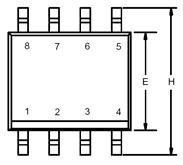
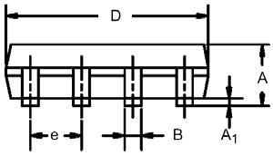
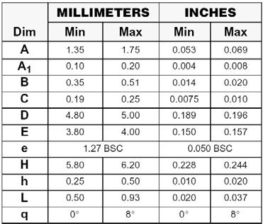
5 Package Information SO-8: 8LEAD H x 45 5
6 Ordering information -T-XX A: Analog Power M: MOSFET 9435: Part number P: P-Channel T: Tape & reel XX: Blank: Standard PF: Leadfree 6
AM6930N. Analog Power Dual N-Channel 30-V (D-S) MOSFET THERMAL RESISTANCE RATINGS. Symbol Maximum Units
 MOSFET THERMAL RESISTANCE RATINGS. Symbol Maximum Units") Dual N-Channel 3-V (D-S) MOSFET These miniature surface mount MOSFETs utilize High Cell Density process. Low r DS(on) assures minimal power loss and conserves energy, making this device ideal for use in
Dual N-Channel 3-V (D-S) MOSFET These miniature surface mount MOSFETs utilize High Cell Density process. Low r DS(on) assures minimal power loss and conserves energy, making this device ideal for use in
AM2306N. Analog Power N-Channel 30-V (D-S) MOSFET. PRODUCT SUMMARY V DS (V) r DS(on) m(ω) I D (A) V GS = 10V V GS = 4.5V 3.
 MOSFET. PRODUCT SUMMARY V DS (V) r DS(on) m(ω) I D (A) V GS = 10V V GS = 4.5V 3.") N-Channel 3-V (D-S) MOSFET These miniature surface mount MOSFETs utilize High Cell Density process. Low r DS(on) assures minimal power loss and conserves energy, making this device ideal for use in power
N-Channel 3-V (D-S) MOSFET These miniature surface mount MOSFETs utilize High Cell Density process. Low r DS(on) assures minimal power loss and conserves energy, making this device ideal for use in power
AM4835P. Analog Power P-Channel 30-V (D-S) MOSFET THERMAL RESISTANCE RATINGS. Symbol Maximum Units
 MOSFET THERMAL RESISTANCE RATINGS. Symbol Maximum Units") P-Channel 3-V (D-S) MOSFET These miniature surface mount MOSFETs utilize High Cell Density process. Low r DS(on) assures minimal power loss and conserves energy, making this device ideal for use in power
P-Channel 3-V (D-S) MOSFET These miniature surface mount MOSFETs utilize High Cell Density process. Low r DS(on) assures minimal power loss and conserves energy, making this device ideal for use in power
THERMAL RESISTANCE RATINGS Parameter Symbol Maximum Units
 P-Channel -V (D-S) MOSFET These miniature surface mount MOSFETs utilize a high cell density trench process to provide low r DS(on) and to ensure minimal power loss and heat dissipation. Typical applications
AM3932N. Analog Power N-Channel 30-V (D-S) MOSFET. PRODUCT SUMMARY V DS (V) r DS(on) m(ω) I D (A) V GS = 4.5V V GS = 2.5V 3.
 MOSFET. PRODUCT SUMMARY V DS (V) r DS(on) m(ω) I D (A) V GS = 4.5V V GS = 2.5V 3.") N-Channel 3-V (D-S) MOSFET These miniature surface mount MOSFETs utilize a high cell density trench process to provide low r DS(on) and to ensure minimal power loss and heat dissipation. Typical applications
N-Channel 3-V (D-S) MOSFET These miniature surface mount MOSFETs utilize a high cell density trench process to provide low r DS(on) and to ensure minimal power loss and heat dissipation. Typical applications
N-Channel 700-V (D-S) MOSFET
 MOSFET") AMN7P N-Channel 7-V (D-S) MOSFET Key Features: Low r DS(on) trench technology Low thermal impedance Fast switching speed PRODUCT SUMMARY r DS(on) (Ω) ID (A) 7 @ V GS = V a VDS (V) Typical Applications:
AMN7P N-Channel 7-V (D-S) MOSFET Key Features: Low r DS(on) trench technology Low thermal impedance Fast switching speed PRODUCT SUMMARY r DS(on) (Ω) ID (A) 7 @ V GS = V a VDS (V) Typical Applications:
P-Channel 60-V (D-S) MOSFET
 MOSFET") AMP6-6B P-Channel 6-V (D-S) MOSFET Key Features: Low r DS(on) trench technology Low thermal impedance Fast switching speed VDS (V) -6 PRODUCT SUMMARY r DS(on) (mω) 6 @ V GS = -V 7 @ V GS = -4.5V ID(A)
AMP6-6B P-Channel 6-V (D-S) MOSFET Key Features: Low r DS(on) trench technology Low thermal impedance Fast switching speed VDS (V) -6 PRODUCT SUMMARY r DS(on) (mω) 6 @ V GS = -V 7 @ V GS = -4.5V ID(A)
N-Channel 100-V (D-S) MOSFET
 MOSFET") AM744NA N-Channel -V (D-S) MOSFET Key Features: Low r DS(on) trench technology Low thermal impedance Fast switching speed VDS (V) PRODUCT SUMMARY r DS(on) (mω) 5 @ V GS = V 7 @ V GS = 4.5V ID (A) 5 4 Typical
AM744NA N-Channel -V (D-S) MOSFET Key Features: Low r DS(on) trench technology Low thermal impedance Fast switching speed VDS (V) PRODUCT SUMMARY r DS(on) (mω) 5 @ V GS = V 7 @ V GS = 4.5V ID (A) 5 4 Typical
AM4825P. Analog Power P-Channel 30-V (D-S) MOSFET THERMAL RESISTANCE RATINGS. Symbol Maximum Units
 MOSFET THERMAL RESISTANCE RATINGS. Symbol Maximum Units") P-Channel 3-V (D-S) MOSFET These miniature surface mount MOSFETs utilize a high cell density trench process to provide low r DS(on) and to ensure minimal power loss and heat dissipation. Typical applications
P-Channel 3-V (D-S) MOSFET These miniature surface mount MOSFETs utilize a high cell density trench process to provide low r DS(on) and to ensure minimal power loss and heat dissipation. Typical applications
N-Channel Logic Level MOSFET
 These miniature surface mount MOSFETs utilize a high cell density trench process to provide low r DS(on) and to ensure minimal power loss and heat dissipation. Typical applications are DC-DC converters
N-Channel 30-V (D-S) MOSFET
 MOSFET") AM734N N-Channel 3-V (D-S) MOSFET Key Features: Low r DS(on) trench technology Low thermal impedance Fast switching speed VDS (V) 3 PRODUCT SUMMARY r DS(on) (mω) @ V GS = V 3 @ V GS = 4.5V ID(A) 6 4 Typical
AM734N N-Channel 3-V (D-S) MOSFET Key Features: Low r DS(on) trench technology Low thermal impedance Fast switching speed VDS (V) 3 PRODUCT SUMMARY r DS(on) (mω) @ V GS = V 3 @ V GS = 4.5V ID(A) 6 4 Typical
P-Channel 20-V (D-S) MOSFET
 MOSFET") AM3PE P-Channel -V (D-S) MOSFET Key Features: Low r DS(on) trench technology Low thermal impedance Fast switching speed VDS (V) - PRODUCT SUMMARY r DS(on) (mω) 8 @ V GS = -.5V @ V GS = -.5V ID (A) -5.6
AM3PE P-Channel -V (D-S) MOSFET Key Features: Low r DS(on) trench technology Low thermal impedance Fast switching speed VDS (V) - PRODUCT SUMMARY r DS(on) (mω) 8 @ V GS = -.5V @ V GS = -.5V ID (A) -5.6
N-Channel 20-V (D-S) MOSFET
 MOSFET") N-Channel -V (D-S) MOSFET Key Features: Low r DS(on) trench technology Low thermal impedance Fast switching speed VDS (V) PRODUCT SUMMARY r DS(on) (mω) @ V GS =.5V @ V GS =.5V ID(A) 7..5 Typical Applications:
N-Channel -V (D-S) MOSFET Key Features: Low r DS(on) trench technology Low thermal impedance Fast switching speed VDS (V) PRODUCT SUMMARY r DS(on) (mω) @ V GS =.5V @ V GS =.5V ID(A) 7..5 Typical Applications:
Dual N-Channel 20-V (D-S) MOSFET
 MOSFET") Dual N-Channel -V (D-S) MOSFET Key Features: Low r DS(on) trench technology Low thermal impedance Fast switching speed VDS (V) PRODUCT SUMMARY r DS(on) (mω) @ V GS =.5V @ V GS =.5V ID (A) Typical Applications:
Dual N-Channel -V (D-S) MOSFET Key Features: Low r DS(on) trench technology Low thermal impedance Fast switching speed VDS (V) PRODUCT SUMMARY r DS(on) (mω) @ V GS =.5V @ V GS =.5V ID (A) Typical Applications:
P-Channel 150-V (D-S) MOSFET
 MOSFET") AM9P P-Channel 5-V (D-S) MOSFET Key Features: Low r DS(on) trench technology Low thermal impedance Fast switching speed VDS (V) -5 PRODUCT SUMMARY r DS(on) (Ω). @ V GS = -V. @ V GS = -4.5V ID(A) -.9 -.8
AM9P P-Channel 5-V (D-S) MOSFET Key Features: Low r DS(on) trench technology Low thermal impedance Fast switching speed VDS (V) -5 PRODUCT SUMMARY r DS(on) (Ω). @ V GS = -V. @ V GS = -4.5V ID(A) -.9 -.8
Analog Power AM3904N. Dual N-Channel Logic Level MOSFET
 Dual N-Channel Logic Level MOSFET These miniature surface mount MOSFETs utilize High Cell Density process. Low r DS(on) assures minimal power loss and conserves energy, making this device ideal for use
FDN327N FDN327N. N-Channel 1.8 Vgs Specified PowerTrench MOSFET. Absolute Maximum Ratings
 N-Channel.8 Vgs Specified PowerTrench MOSFET General Description This V N-Channel MOSFET uses ON Semiconductor s high voltage PowerTrench process. It has been optimized for power management applications.
Features D G. T A =25 o C unless otherwise noted. Symbol Parameter Ratings Units. (Note 1a) 3.8. (Note 1b) 1.6
 3.8. (Note 1b) 1.6") FDD564P 6V P-Channel PowerTrench MOSFET FDD564P General Description This 6V P-Channel MOSFET uses ON Semiconductor s high voltage PowerTrench process. It has been optimized for power management applications.
FDD564P 6V P-Channel PowerTrench MOSFET FDD564P General Description This 6V P-Channel MOSFET uses ON Semiconductor s high voltage PowerTrench process. It has been optimized for power management applications.
PUBLICATION ORDERING INFORMATION. Semiconductor Components Industries, LLC
 FDS39 FDS39 V N-Channel Dual PowerTrench MOSFET General Description This N-Channel MOSFET has been designed specifically to improve the overall efficiency of DC/DC converters using either synchronous or
FDS8935. Dual P-Channel PowerTrench MOSFET. FDS8935 Dual P-Channel PowerTrench MOSFET. -80 V, -2.1 A, 183 mω
 FDS935 Dual P-Channel PowerTrench MOSFET - V, -. A, 3 mω Features Max r DS(on) = 3 mω at V GS = - V, I D = -. A Max r DS(on) = 7 mω at V GS = -.5 V, I D = -.9 A High performance trench technology for extremely
Features. TA=25 o C unless otherwise noted
 NDS6 NDS6 P-Channel Enhancement Mode Field Effect Transistor General Description These P-Channel enhancement mode field effect transistors are produced using ON Semiconductor's proprietary, high cell density,
Description. Symbol Parameter FCP260N65S3 Unit V DSS Drain to Source Voltage 650 V
 FCP260N65S3 N-Channel SuperFET III MOSFET 650 V, 2 A, 260 mω Features 700 V @ T J = 50 o C Typ. R DS(on) = 222 mω Ultra Low Gate Charge (Typ. Q g = 24 nc) Low Effective Output Capacitance (Typ. C oss(eff.)
FDN335N N-Channel 2.5V Specified PowerTrench TM MOSFET
 N-Channel.5V Specified PowerTrench TM MOSFET General Description This N-Channel.5V specified MOSFET is produced using ON Semiconductor's advanced PowerTrench process that has been especially tailored to
FDMA3028N. Dual N-Channel PowerTrench MOSFET. FDMA3028N Dual N-Channel PowerTrench MOSFET. 30 V, 3.8 A, 68 mω Features. General Description
 FDMA38N Dual N-Channel PowerTrench MOSFET 3 V, 3.8 A, 68 mω Features Max. R DS(on) = 68 mω at V GS =.5 V, I D = 3.8 A Max. R DS(on) = 88 mω at V GS =.5 V, I D = 3. A Max. R DS(on) = 3 mω at V GS =.8 V,
N-Channel Logic Level Enhancement Mode Field Effect Transistor. Features. TA=25 o C unless otherwise noted
 BSS BSS N-Channel Logic Level Enhancement Mode Field Effect Transistor General Description These N-Channel enhancement mode field effect transistors are produced using ON Semiconductor s proprietary, high
FDP8D5N10C / FDPF8D5N10C/D
 FDP8D5NC / FDPF8D5NC N-Channel Shielded Gate PowerTrench MOSFET V, 76 A, 8.5 mω Features Max r DS(on) = 8.5 mω at V GS = V, I D = 76 A Extremely Low Reverse Recovery Charge, Qrr % UIL Tested RoHS Compliant
Is Now Part of To learn more about ON Semiconductor, please visit our website at
 Is Now Part of To learn more about ON Semiconductor, please visit our website at www.onsemi.com ON Semiconductor and the ON Semiconductor logo are trademarks of Semiconductor Components Industries, LLC
FDS8949 Dual N-Channel Logic Level PowerTrench MOSFET
 FDS899 Dual N-Channel Logic Level PowerTrench MOSFET V, 6A, 9mΩ Features Max r DS(on) = 9mΩ at V GS = V Max r DS(on) = 36mΩ at V GS =.5V Low gate charge High performance trench technology for extremely
Extended V GSS range ( 25V) for battery applications
 for battery applications") Dual Volt P-Channel PowerTrench MOSFET General Description This P-Channel MOSFET has been designed specifically to improve the overall efficiency of DC/DC converters using either synchronous or conventional
Dual Volt P-Channel PowerTrench MOSFET General Description This P-Channel MOSFET has been designed specifically to improve the overall efficiency of DC/DC converters using either synchronous or conventional
Applications. Inverter H-Bridge. G1 S1 N-Channel. S1 Dual DPAK 4L
 FDD35H Dual N & P-Channel PowerTrench MOSFET N-Channel: V, 3.9A, mω P-Channel: -V, -9.A, 9mΩ Features Q: N-Channel Max r DS(on) = mω at V GS = V, I D =.3A Max r DS(on) = mω at V GS = V, I D =.A : P-Channel
N-Channel Logic Level PowerTrench MOSFET
 FDN56N-F85 N-Channel Logic Level PowerTrench MOSFET 6 V,.6 A, 98 mω Features R DS(on) = 98 mω at V GS = 4.5 V, I D =.6 A R DS(on) = 8 mω at V GS = V, I D =.7 A Typ Q g(tot) = 9. nc at V GS = V Low Miller
Description. Symbol Parameter FCMT180N65S3 Unit V DSS Drain to Source Voltage 650 V. - Continuous (T C = 25 o C) 17 - Continuous (T C = 100 o C) 11
 17 - Continuous (T C = 100 o C) 11") FCMT80N65S3 N-Channel SUPERFET III Easy-Drive MOSFET 650 V, 7 A, 80 mω Features 700 V @ T J = 50 o C Typ. R DS(on) = 52 mω Ultra Low Gate Charge (Typ. Q g = 33 nc) Low Effective Output Capacitance (Typ.
FCMT80N65S3 N-Channel SUPERFET III Easy-Drive MOSFET 650 V, 7 A, 80 mω Features 700 V @ T J = 50 o C Typ. R DS(on) = 52 mω Ultra Low Gate Charge (Typ. Q g = 33 nc) Low Effective Output Capacitance (Typ.
NTGS3441BT1G. Power MOSFET. -20 V, -3.5 A, Single P-Channel, TSOP-6. Low R DS(on) in TSOP-6 Package 2.5 V Gate Rating This is a Pb-Free Device
 in TSOP-6 Package 2.5 V Gate Rating This is a Pb-Free Device") Power MOSFET - V, -. A, Single P-Channel, TSOP- Features Low R DS(on) in TSOP- Package. V Gate Rating This is a Pb-Free Device Applications Battery Switch and Load Management Applications in Portable Equipment
Power MOSFET - V, -. A, Single P-Channel, TSOP- Features Low R DS(on) in TSOP- Package. V Gate Rating This is a Pb-Free Device Applications Battery Switch and Load Management Applications in Portable Equipment
N & P-Channel 100-V (D-S) MOSFET
 MOSFET") N & P-Channel -V (D-S) MOSFET Key Features: Low r DS(on) trench technology Low thermal impedance Fast switching speed Typical Applications: LED Inverter Circuits DC/DC Conversion Circuits Motor drives
N & P-Channel -V (D-S) MOSFET Key Features: Low r DS(on) trench technology Low thermal impedance Fast switching speed Typical Applications: LED Inverter Circuits DC/DC Conversion Circuits Motor drives
NTH027N65S3F N-Channel SuperFET III FRFET MOSFET 650 V, 75 A, 27.4 mω Features
 NTH027N65S3F N-Channel SuperFET III FRFET MOSFET 650 V, 75 A, 27.4 mω Features 700 V @ T J = 50 o C Typ. R DS(on) = 23 mω Ultra Low Gate Charge (Typ. Q g = 259 nc) Low Effective Output Capacitance (Typ.
NTA4001N, NVA4001N. Small Signal MOSFET. 20 V, 238 ma, Single, N Channel, Gate ESD Protection, SC 75
 Small Signal MOSFET V, 8 ma, Single, N Channel, Gate ESD Protection, SC 75 Features Low Gate Charge for Fast Switching Small.6 x.6 mm Footprint ESD Protected Gate AEC Q Qualified and PPAP Capable NVA4N
FDPC4044. Common Drain N-Channel PowerTrench MOSFET. FDPC4044 Common Drain N-Channel PowerTrench MOSFET. 30 V, 27 A, 4.
 FDPC444 Common Drain N-Channel PowerTrench MOSFET 3 V, 7 A, 4.3 mω Features Max r SS(on) = 4.3 mω at V GS = V, I SS = 7 A Max r SS(on) = 6.4 mω at V GS = 4.5 V, I SS = 3 A Pakage size/height: 3.3 x 3.3
Bottom. Pin 1 S S S D D D. Symbol Parameter Ratings Units V DS Drain to Source Voltage 30 V V GS Gate to Source Voltage (Note 4) ±20 V
 ±20 V") D D D FDMS7658AS N-Channel PowerTrench SyncFET TM 3 V, 76 A,.9 mω Features Max r DS(on) =.9 mω at V GS = V, I D = 8 A Max r DS(on) =. mω at V GS = 7 V, I D = 6 A Advanced Package and Silicon Combination
D D D FDMS7658AS N-Channel PowerTrench SyncFET TM 3 V, 76 A,.9 mω Features Max r DS(on) =.9 mω at V GS = V, I D = 8 A Max r DS(on) =. mω at V GS = 7 V, I D = 6 A Advanced Package and Silicon Combination
NTNUS3171PZ. Small Signal MOSFET. 20 V, 200 ma, Single P Channel, 1.0 x 0.6 mm SOT 1123 Package
 NTNUS7PZ Small Signal MOSFET V, ma, Single P Channel,. x.6 mm SOT Package Features Single P Channel MOSFET Offers a Low R DS(on) Solution in the Ultra Small. x.6 mm Package. V Gate Voltage Rating Ultra
NVC6S5A444NLZ. Power MOSFET. 60 V, 78 m, 4.5 A, N Channel
 Power MOSFET 6 V, 78 m,.5 A, N Channel Automotive Power MOSFET designed to minimize gate charge and low on resistance. AEC Q qualified MOSFET and PPAP capable suitable for automotive applications. Features.5
Is Now Part of To learn more about ON Semiconductor, please visit our website at
 Is Now Part of To learn more about ON Semiconductor, please visit our website at www.onsemi.com ON Semiconductor and the ON Semiconductor logo are trademarks of Semiconductor Components Industries, LLC
NTLUS3A90PZ. Power MOSFET 20 V, 5.0 A, Cool Single P Channel, ESD, 1.6x1.6x0.55 mm UDFN Package
 NTLUS3A9PZ Power MOSFET V, 5. A, Cool Single P Channel, ESD,.x.x.55 mm UDFN Package Features UDFN Package with Exposed Drain Pads for Excellent Thermal Conduction Low Profile UDFN.x.x.55 mm for Board Space
CPH6354. Power MOSFET 60V, 100mΩ, 4A, Single P-Channel. Features. Specifications
 CPH64 Power MOSFET 6V, 1mΩ, 4A, Single P-Channel Features ON-resistance RDS(on)1=mW(typ.) 4V Drive ESD Diode - Protected Gate Pb-Free, Halogen Free and RoHS Compliance Specifications Absolute Maximum Ratings
NTGD4167C. Power MOSFET Complementary, 30 V, +2.9/ 2.2 A, TSOP 6 Dual
 Power MOSFET Complementary, 3 V, +.9/. A, TSOP 6 Dual Features Complementary N Channel and P Channel MOSFET Small Size (3 x 3 mm) Dual TSOP 6 Package Leading Edge Trench Technology for Low On Resistance
NTNS3164NZT5G. Small Signal MOSFET. 20 V, 361 ma, Single N Channel, SOT 883 (XDFN3) 1.0 x 0.6 x 0.4 mm Package
 1.0 x 0.6 x 0.4 mm Package") NTNS36NZ Small Signal MOSFET V, 36 ma, Single N Channel, SOT 883 (XDFN3). x.6 x. mm Package Features Single N Channel MOSFET Ultra Low Profile SOT 883 (XDFN3). x.6 x. mm for Extremely Thin Environments
NTNS36NZ Small Signal MOSFET V, 36 ma, Single N Channel, SOT 883 (XDFN3). x.6 x. mm Package Features Single N Channel MOSFET Ultra Low Profile SOT 883 (XDFN3). x.6 x. mm for Extremely Thin Environments
FDD8444L-F085 N-Channel PowerTrench MOSFET
 M E N FDD8444L-F85 N-Channel PowerTrench MOSFET 4V, 5A, 6.mΩ Features Applications Typ r DS(on) = 3.8mΩ at V GS = 5V, I D = 5A Automotive Engine Control Typ Q g(tot) = 46nC at V GS = 5V Powertrain Management
Dual N-Channel, Digital FET
 FDG6301N-F085 Dual N-Channel, Digital FET Features 25 V, 0.22 A continuous, 0.65 A peak. R DS(ON) = 4 @ V GS = 4.5 V, R DS(ON) = 5 @ V GS = 2.7 V. Very low level gate drive requirements allowing directoperation
NTS4173PT1G. Power MOSFET. 30 V, 1.3 A, Single P Channel, SC 70
 NTS17P Power MOSFET V, 1. A, Single P Channel, SC 7 Features V BV ds, Low R DS(on) in SC 7 Package Low Threshold Voltage Fast Switching Speed This is a Halide Free Device This is a Pb Free Device Applications
Features. Symbol Parameter Ratings Units V DSS Drain-Source Voltage -40 V
 FDS4675-F085 40V P-Channel PowerTrench MOSFET General Description This P-Channel MOSFET is a rugged gate version of ON Semiconductor s advanced Power Tranch process. It has been optimized for power management
Is Now Part of To learn more about ON Semiconductor, please visit our website at
 Is Now Part of To learn more about ON Semiconductor, please visit our website at www.onsemi.com ON Semiconductor and the ON Semiconductor logo are trademarks of Semiconductor Components Industries, LLC
Features S 1. TA=25 o C unless otherwise noted
 FC5P V P-Channel Logic Level PowerTrench MOSFET FC5P General escription This V P-Channel MOSFET uses ON Semiconductor s high voltage PowerTrench process. It has been optimized for power management applications.
NTMD4184PFR2G. Power MOSFET and Schottky Diode -30 V, -4.0 A, Single P-Channel with 20 V, 2.2 A, Schottky Barrier Diode Features
 NTMDPF Power MOSFET and Schottky Diode -3 V, -. A, Single P-Channel with V,. A, Schottky Barrier Diode Features FETKY Surface Mount Package Saves Board Space Independent Pin-Out for MOSFET and Schottky
FDD V P-Channel POWERTRENCH MOSFET
 3 V P-Channel POWERTRENCH MOSFET General Description This P Channel MOSFET is a rugged gate version of ON Semiconductor s advanced POWERTRENCH process. It has been optimized for power management applications
N-Channel PowerTrench MOSFET
 FDBL86363-F85 N-Channel PowerTrench MOSFET 8 V, 4 A,. mω Features Typical R DS(on) =.5 mω at V GS = V, I D = 8 A Typical Q g(tot) = 3 nc at V GS = V, I D = 8 A UIS Capability RoHS Compliant Qualified to
ACE3006M N-Channel Enhancement Mode MOSFET
 Description uses advanced trench technology to provide excellent R DS(ON). This device particularly suits for low voltage application such as power management of desktop computer or notebook computer power
NTJS4405N, NVJS4405N. Small Signal MOSFET. 25 V, 1.2 A, Single, N Channel, SC 88
 NTJSN, NVJSN Small Signal MOSFET V,. A, Single, N Channel, SC 88 Features Advance Planar Technology for Fast Switching, Low R DS(on) Higher Efficiency Extending Battery Life AEC Q Qualified and PPAP Capable
NTS4172NT1G. Power MOSFET. 30 V, 1.7 A, Single N Channel, SC 70. Low On Resistance Low Gate Threshold Voltage Halide Free This is a Pb Free Device
 Power MOSFET V,.7 A, Single N Channel, SC 7 Features Low On Resistance Low Gate Threshold Voltage Halide Free This is a Pb Free Device V (BR)DSS R DS(on) MAX I D MAX Applications Low Side Load Switch DC
Description. Symbol Parameter FCH041N65EF-F155 Unit V DSS Drain to Source Voltage 650 V
 FCH04N65EF N-Channel SuperFET II FRFET MOSFET 650 V, 76 A, 4 mω Features 700 V @ T J = 50 C Typ. R DS(on) = 36 mω Ultra Low Gate Charge (Typ. Q g = 229 nc) Low Effective Output Capacitance (Typ. C oss(eff.)
NTLJD4116NT1G. Power MOSFET. 30 V, 4.6 A, Cool Dual N Channel, 2x2 mm WDFN Package
 NTLJDN Power MOSFET V,. A, Cool Dual N Channel, x mm WDFN Package Features WDFN Package Provides Exposed Drain Pad for Excellent Thermal Conduction x mm Footprint Same as SC 88 Lowest R DS(on) Solution
This product is designed to ESD immunity < 200V*, so please take care when handling. * Machine Model
 1HN4CH Power MOSFET V, 8Ω, ma, Single N-Channel http://onsemi.com Features 4V drive Halogen free compliance Specifications Absolute Maximum Ratings at Ta = C Parameter Symbol Conditions Value Unit Drain
MCH6664. P-Channel Power MOSFET 30V, 1.5A, 325mΩ, Dual MCPH6. Features
 Ordering number : ENA81A MCH6664 P-Channel Power MOSFET V, 1.A, mω, Dual MCPH6 http://onsemi.com Features ON-resistance Pch : RDS(on)1=mW (typ.) 4V drive Halogen free compliance Specifications Absolute
N-Channel PowerTrench MOSFET
 FDMS86369-F85 N-Channel PowerTrench MOSFET 8 V, 65 A, 7.5 mω Features Typical R DS(on) = 5.9 mω at V GS = V, I D = 65 A Typical Q g(tot) = 35 nc at V GS = V, I D = 65 A UIS Capability RoHS Compliant Qualified
FDS8984 N-Channel PowerTrench MOSFET 30V, 7A, 23mΩ
 FDS898 N-Channel PowerTrench MOSFET V, 7A, 3mΩ General Description This N-Channel MOSFET has been designed specifically to improve the overall efficiency of DC/DC converters using either synchronous or
N-Channel SuperFET MOSFET
 FCD5N-F5 N-Channel SuperFET MOSFET V,. A,. Ω Features V,.A, typ. R ds(on) =mω@v GS =V Ultra Low Gate Charge (Typ. Q g = nc) UIS Capability RoHS Compliant Qualified to AEC Q Applications Automotive On Board
NTD7N ELECTRICAL CHARACTERISTICS ( unless otherwise stated) Parameter Symbol Test Condition Min Typ Max Unit OFF CHARACTERISTICS Drain to Source Break
 Parameter Symbol Test Condition Min Typ Max Unit OFF CHARACTERISTICS Drain to Source Break") NTD7N Power MOSFET V, 8 A, Single N Channel, Features Low R DS(on) High Current Capability Low Gate Charge These are Pb Free Devices Applications Electronic Brake Systems Electronic Power Steering Bridge
NTD7N Power MOSFET V, 8 A, Single N Channel, Features Low R DS(on) High Current Capability Low Gate Charge These are Pb Free Devices Applications Electronic Brake Systems Electronic Power Steering Bridge
NTLUD3A260PZ. Power MOSFET 20 V, 2.1 A, Cool Dual P Channel, ESD, 1.6x1.6x0.55 mm UDFN Package
 NTLUDAPZ Power MOSFET V,. A, Cool Dual P Channel, ESD,.x.x. mm UDFN Package Features UDFN Package with Exposed Drain Pads for Excellent Thermal Conduction Low Profile UDFN.x.x. mm for Board Space Saving
Is Now Part of. To learn more about ON Semiconductor, please visit our website at
 Is Now Part of To learn more about ON Semiconductor, please visit our website at www.onsemi.com Please note: As part of the Fairchild Semiconductor integration, some of the Fairchild orderable part numbers
NTTFS5116PLTWG. Power MOSFET 60 V, 20 A, 52 m. Low R DS(on) Fast Switching These Devices are Pb Free and are RoHS Compliant
 Fast Switching These Devices are Pb Free and are RoHS Compliant") Power MOSFET 6 V, 2 A, 52 m Features Low R DS(on) Fast Switching These Devices are Pb Free and are RoHS Compliant Applications Load Switches DC Motor Control DC DC Conversion MAXIMUM RATINGS ( unless otherwise
Power MOSFET 6 V, 2 A, 52 m Features Low R DS(on) Fast Switching These Devices are Pb Free and are RoHS Compliant Applications Load Switches DC Motor Control DC DC Conversion MAXIMUM RATINGS ( unless otherwise
P-Channel PowerTrench MOSFET
 FDD4685-F085 P-Channel PowerTrench MOSFET -40 V, -32 A, 35 mω Features Typical R DS(on) = 23 m at V GS = -10V, I D = -8.4 A Typical R DS(on) = 30 m at V GS = -4.5V, I D = -7 A Typical Q g(tot) = 19 nc
Is Now Part of To learn more about ON Semiconductor, please visit our website at
 Is Now Part of To learn more about ON Semiconductor, please visit our website at www.onsemi.com ON Semiconductor and the ON Semiconductor logo are trademarks of Semiconductor Components Industries, LLC
ZXMHC10A07N8 100V SO8 Complementary enhancement mode MOSFET H-Bridge
 A Product Line of Diodes Incorporated ZXMHC0A07N8 00V SO8 Complementary enhancement mode MOSFET H-Bridge Summary Device V (BR)DSS Q G R DS(on) I D T A = 25 C N-CH 00V 2.9nC 0.70Ω @ = 0V.0A 0.90Ω @ = 6.0V
ZXMC10A816N8 100V SO8 Complementary Dual enhancement mode MOSFET
 A Product Line of Diodes Incorporated ZXMCA86N8 0V SO8 Complementary Dual enhancement mode MOSFET Summary Device V (BR)DSS (V) Q G (nc) R DS(on) (Ω) (A) T A = 25 C Q 0 9.2 0.230 @ = V 2. 0.300 @ =.9 Q2-0
3000/Tape&Reel. 2 P D Maximum Power Dissipation TA = 75 o C 1.44 T J, T stg Operating Junction and Storage Temperature Range
 DS = 30 R DS(ON), gs @10, I ds @8.5A = 38mΩ R DS(ON), gs @4.5, I ds @5A = 52mΩ Features Advanced trench process technology High Density Cell Design For Ultra Low On-Resistance High Power and Current Handling
Is Now Part of To learn more about ON Semiconductor, please visit our website at
 Is Now Part of To learn more about ON Semiconductor, please visit our website at www.onsemi.com ON Semiconductor and the ON Semiconductor logo are trademarks of Semiconductor Components Industries, LLC
Description. Symbol Parameter Ratings Units V DSS Drain to Source Voltage 500 V V GSS Gate to Source Voltage ±30 V
 FDD5N50FTM-WS N-Channel UniFET TM FRFET MOSFET 500 V, 3.5 A,.55 Ω Features R DS(on) =.25Ω (Typ.) @ V GS = 0 V, I D =.75 A Low Gate Charge (Typ. nc) Low C rss (Typ. 5 pf) Fast Switching 00% Avalanche Tested
FDPF18N20FT-G N-Channel UniFET TM FRFET MOSFET
 FDPF8N20FT-G N-Channel UniFET TM FRFET MOSFET 200 V, 8 A, 40 m Features R DS(on) = 29 mω (Typ.) @ V GS = 0 V, I D = 9 A Low Gate Charge (Typ. 20 nc) Low C rss (Typ. 24 pf) 00% Avalanche Tested Improve
N-Channel PowerTrench MOSFET
 FDBL8636-F85 N-Channel PowerTrench MOSFET 8 V, 3 A,.4 mω Features Typical R DS(on) =. mω at V GS = V, I D = 8 A Typical Q g(tot) = 72 nc at V GS = V, I D = 8 A UIS Capability RoHS Compliant Qualified to
NTLUF4189NZ Power MOSFET and Schottky Diode
 NTLUF89NZ Power MOSFET and Schottky Diode V, N Channel with. A Schottky Barrier Diode,. x. x. mm Cool Package Features Low Qg and Capacitance to Minimize Switching Losses Low Profile UDFN.x. mm for Board
ZXMHC3A01N8 30V SO8 Complementary enhancement mode MOSFET H-Bridge
 A Product Line of Diodes Incorporated ZXMHC3A0N8 30V SO8 Complementary enhancement mode MOSFET H-Bridge Summary Device V (BR)DSS Q G R DS(on) I D T A = 25 C N-CH 30V 3.9nC 25m @ = 0V 2.7A 80m @ = 4. 2.2A
NVLJD4007NZTBG. Small Signal MOSFET. 30 V, 245 ma, Dual, N Channel, Gate ESD Protection, 2x2 WDFN Package
 NVLJD7NZ Small Signal MOSFET V, 2 ma, Dual, N Channel, Gate ESD Protection, 2x2 WDFN Package Features Optimized Layout for Excellent High Speed Signal Integrity Low Gate Charge for Fast Switching Small
RM4503S8. N and P-Channel Enhancement Mode Power MOSFET. Description. General Features. Application. Package Marking and Ordering Information
 RM4503S8 N and P-Channel Enhancement Mode Power MOSFET Description The RM4503S8 uses advanced trench technology to provide excellent R DS(ON) and low gate charge. The SOP-8 package is universally preferred
MCH6662. Power MOSFET 20V, 160mΩ, 2A, Dual N-Channel. Features. Specifications
 MCH666 Power MOSFET V, 16mΩ, A, Dual N-Channel Features ON-Resistance Nch : RDS(on)1=1mW (typ) 1.8V Drive ESD Diode - Protected Gate Pb-Free, Halogen Free and RoHS Compliance Specifications Absolute Maximum
P-Channel PowerTrench MOSFET -40V, -14A, 64mΩ
 FDD4243-F85 P-Channel PowerTrench MOSFET -V, -4A, 64mΩ Features Typ r DS(on) = 36m at V GS = -V, I D = -6.7A Typ r DS(on) = 48m at V GS = -4.5V, I D = -5.5A Typ Q g(tot) = 2nC at V GS = -V High performance
NTTFS5820NLTWG. Power MOSFET. 60 V, 37 A, 11.5 m. Low R DS(on) Low Capacitance Optimized Gate Charge These Devices are Pb Free and are RoHS Compliant
 Low Capacitance Optimized Gate Charge These Devices are Pb Free and are RoHS Compliant") NTTFS582NL Power MOSFET 6 V, 37 A,.5 m Features Low R DS(on) Low Capacitance Optimized Gate Charge These Devices are Pb Free and are RoHS Compliant MAXIMUM RATINGS ( unless otherwise stated) Parameter
NTTFS582NL Power MOSFET 6 V, 37 A,.5 m Features Low R DS(on) Low Capacitance Optimized Gate Charge These Devices are Pb Free and are RoHS Compliant MAXIMUM RATINGS ( unless otherwise stated) Parameter
NTHD4502NT1G. Power MOSFET. 30 V, 3.9 A, Dual N Channel ChipFET
 NTHDN Power MOSFET V,.9 A, Dual N Channel ChipFET Features Planar Technology Device Offers Low R DS(on) and Fast Switching Speed Leadless ChipFET Package has % Smaller Footprint than TSOP. Ideal Device
ELECTRICAL CONNECTION
 Power MOSFET 30V, 215mΩ, 2.0A, Single P-Channel This Power MOSFET is produced using ON Semiconductor s trench technology, which is specifically designed to minimize gate charge and low on resistance. This
CPH3360. Power MOSFET 30V, 303mΩ, 1.6A, Single P-Channel
 Power MOSFET 30V, 303mΩ, 1.6A, Single P-Channel This Power MOSFET is produced using ON Semiconductor s trench technology, which is specifically designed to minimize gate charge and low on resistance. This
NTMD4820NR2G. Power MOSFET 30 V, 8 A, Dual N Channel, SOIC 8
 NTMDN Power MOSFET V, A, Dual N Channel, SOIC Features Low R DS(on) to Minimize Conduction Losses Low Capacitance to Minimize Driver Losses Optimized Gate Charge to Minimize Switching Losses Dual SOIC
MCH3382. Power MOSFET 12V, 198mΩ, 2A, Single P-Channel
 Power MOSFET 12V, 198mΩ, 2A, Single P-Channel This Power MOSFET is produced using ON Semiconductor s trench technology, which is specifically designed to minimize gate charge and low on resistance. This
NTMS5835NL. Power MOSFET 40 V, 12 A, 10 m
 Power MOSFET V, 2 A, m Features Low R DS(on) Low Capacitance Optimized Gate Charge These Devices are Pb Free, Halogen Free/BFR Free and are RoHS Compliant MAXIMUM RATINGS ( unless otherwise stated) Parameter
MCH3383. Power MOSFET 12V, 69mΩ, 3.5A, Single P-Channel
 Power MOSFET 12V, 69mΩ, 3.5A, Single P-Channel This Power MOSFET is produced using ON Semiconductor s trench technology, which is specifically designed to minimize gate charge and low on resistance. This
NTS2101P. Power MOSFET. 8.0 V, 1.4 A, Single P Channel, SC 70
 NTS11P Power MOSFET 8. V, 1.4 A, Single P Channel, SC 7 Features Leading Trench Technology for Low R DS(on) Extending Battery Life 1.8 V Rated for Low Voltage Gate Drive SC 7 Surface Mount for Small Footprint
1HP04CH. Small Signal MOSFET 100V, 18Ω, 170mA, Single P-Channel
 Small Signal MOSFET 100V, 18Ω, 170mA, Single P-Channel This Power MOSFET is produced using ON Semiconductor s trench technology, which is specifically designed to minimize gate charge and low on resistance.
ACE2020M N-Channel 200-V MOSFET
 Description ACE2020M uses advanced trench technology to provide excellent R DS(ON). This device particularly suits for low voltage application such as power management of desktop computer or notebook computer
PIN CONNECTIONS MAXIMUM RATINGS (T J = 25 C unless otherwise noted) SC 75 (3 Leads) Parameter Symbol Value Unit Drain to Source Voltage V DSS 30 V
 SC 75 (3 Leads) Parameter Symbol Value Unit Drain to Source Voltage V DSS 30 V") NTA7N, NVTA7N Small Signal MOSFET V, 4 ma, Single, N Channel, Gate ESD Protection, SC 7 Features Low Gate Charge for Fast Switching Small.6 x.6 mm Footprint ESD Protected Gate NV Prefix for Automotive
NTA7N, NVTA7N Small Signal MOSFET V, 4 ma, Single, N Channel, Gate ESD Protection, SC 7 Features Low Gate Charge for Fast Switching Small.6 x.6 mm Footprint ESD Protected Gate NV Prefix for Automotive
NTHD2102PT1G. Power MOSFET. 8.0 V, 4.6 A Dual P Channel ChipFET
 NTHDP Power MOSFET. V,. A Dual PChannel ChipFET Features Offers an Ultra Low R DS(on) Solution in the ChipFET Package Miniature ChipFET Package % Smaller Footprint than TSOP making it an Ideal Device for
MCH6331. Power MOSFET 30V, 98mΩ, 3.5A, Single P-Channel
 Power MOSFET 30V, 98mΩ, 3.5A, Single P-Channel This Power MOSFET is produced using ON Semiconductor s trench technology, which is specifically designed to minimize gate charge and low on resistance. This
NTMS5838NL. Power MOSFET 40 V, 7.5 A, 20 m
 Power MOSFET V, 7.5 A, 2 m Features Low R DS(on) Low Capacitance Optimized Gate Charge These Devices are Pb Free, Halogen Free/BFR Free and are RoHS Compliant MAXIMUM RATINGS ( unless otherwise stated)
High Speed Switching ESD Diode-Protected Gate C/W
 Ordering number : ENA1559B Power MOSFET 60V, 62mΩ, 12A, Single P-Channel http://onsemi.com Features Low On-Resistance Low Gate Charge Pb-free and RoHS Compliance High Speed Switching ESD Diode-Protected
ECH8659. Power MOSFET 30V, 24mΩ, 7A, Dual N-Channel
 Power MOSFET 30V, 24mΩ, 7A, Dual N-Channel This Power MOSFET is produced using ON Semiconductor s trench technology, which is specifically designed to minimize gate charge and low on resistance. This device