A 45-nm SOI-CMOS Dual-PLL Processor Clock System for Multi-Protocol I/O
|
|
|
- Nickolas Poole
- 6 years ago
- Views:
Transcription

1 A 45-nm SOI-CMOS Dual-PLL Processor Clock System for Multi-Protocol I/O Dennis Fischette, Alvin Loke, Michael Oshima, Bruce Doyle, Roland Bakalski*, Richard DeSantis, Anand Thiruvengadam, Charles Wang, Gerry Talbot, Emerson Fang Advanced Micro Devices,Inc., *GlobalFoundries
2 Outline Introduction Architecture and Circuits Ring-based PLL LC-based PLL Silicon Results Conclusion 2
3 The Vision I/O connectivity for integrated CPU + GPU PCI Express (PCIe) 1.1 & 2.0 DisplayPort (DP), DVI, HDMI Monitor Display DP DVI HDMI Integrated CPU + GPU PCIe DDR Off-Chip Memory SouthBridge I/O Controller PCIe devices (audio, video,...) 3
4 Multi-Protocol Requirements Wide range of operating modes f ref = MHz f out = MHz 2 4 MHz < 2 db Peaking 5 8 MHz < 1 db Peaking 8 16 MHz < 3 db Peaking Strict PLL phase jitter requirements < ps rms Fast exit (< 5 µs) from power-down/sleep modes for low-power client applications 4
5 Design Challenges Partially-depleted (PD) SOI noise concerns More FET noise than bulk from floating body and high-resistance body ties More difficult to predict jitter since RF simulators cannot handle floating-body devices correctly PVT variation + mismatch large BW variation e.g., 3x VCO gain variation Noisy operating environment Multi-core CPU + graphics + memory controller 5
6 Outline Introduction Architecture and Circuits Ring-based PLL LC-based PLL Silicon Results Conclusion 6
7 Dual-PLL Architecture Low-jitter LC-PLL for PCIe 2.0 (narrow tuning range) Higher-jitter Ring-PLL for all other modes (wide tuning range) 10% area overhead for dual-plls (many shared circuits) Voltage regulators (from 2.5 V) to reduce power-supply noise 7
8 Ring-PLL Dual-Path VCO Control High-BW / low-gain path (V control ) Sets PLL bandwidth Conventional 2-pole / 1-zero Effective K VCO jitter (70% less jitter contribution from loop-filter resistor and charge-pump) Low-BW / high-gain path (V slow ) Sets VCO center frequency BW (V slow ) < 0.2% BW (V control ) Contributes negligible jitter Bypass R slow during fastlock mode (pay attention to stability) IR drop across R slow due to leakage < 15 mv limits BW (V slow ) 8
9 Ring-PLL Slow-Path Jitter Analysis Low-pass filter shapes noise to control jitter 1 Vn C R slow slow For constant RC, get lower jitter with larger C slow but area penalty R slow = 600 kω and C slow = 20 pf Negligible slow-path jitter Slow-path jitter < 75 fs Fast-path jitter < 400 fs VCO jitter < 1000 fs Relative RMS Phase Jitter 2.5 R slow C slow = constant Relative C slow 9
10 Ring-PLL VCO Design Dual-control path for lower effective gain Body-tied MOSFETs for jitter reduction and ability to simulate 2x speed penalty 5-stage Ring-oscillator VCO 5 stages for easier oscillation Cross-coupled inverters for fast slew rates and level shifting Source degeneration in current bias for noise reduction Amplifier in bias circuits to improve supply noise rejection Divide-by-2 50% duty-cycle VCO V-to-I Converter V control V slow 1x 3x 5-stage Ring VCO VCO gain control V RO 10
11 Body-Tied PD-SOI MOSFET (T-Gate) Enables body connection to undepleted FET well High R body and extra C gate limits BW of body connection NMOS example p + p + diffusion Poly gate SOI active island p + body-tie n + n + n + source n + drain p-well Lateral connection to undepleted p-well n + diffusion body node 11
12 Ring-PLL VCO Gain Calibration PLL in closed-loop operation with fastlock asserted Algorithm reduce Kv[3:0] until V control > V ref Result K vco variation across PVT reduced by 43% More constant I bias 15% less jitter 9 db lower ref spurs 12
13 Bandwidth and Peaking Measurements Algorithm based on Fischette et al., CICC 2009 Apply instantaneous half-period phase step by inverting RefClk Measure τ crossover ( BW) and MaxOvershoot ( Peaking) Phase Error (ns) MaxOvershoot τ crossover Time (µs) τ crossover (µs s) /BW (µs) MaxOvershoot (ns) Peaking (db) 13
14 LC-PLL 10 GHz LC-VCO Design Lower jitter than ring-vco 29% tuning range Tune at 4x required frequency for smaller L and 50% duty cycle Low VCO gain No slow path required Floorplan to avoid magnetic coupling from switching currents in surrounding circuits and supply bumps fine tuning control 5-bit coarse tuning control Amplitude Control tail bias VCO output 14


15 LC-PLL VCO Elements Body ties for gain and tail devices Narrow widths for higher BW connectivity Lower channel and upconverted 1 / f noise Tuning range penalty from T-gate load Differential inductor M11 turns with M10-M09-M08 underpass Extensive dummy metal fill for CMP manufacturability Varactors Accumulation mode n-well for good Q Thick oxide for low I gate 15
16 LC-PLL Coarse-Tuning Calibration VCO coarse-tuned by 5-bit DAC, steps frequency by % Calibrate VCO using RefClk and PLL feedback clock counters RefClk has up to 0.5% spread spectrum frequency modulation Count over one 33 khz spread spectrum period to desensitize calibration from modulation phase and preserve post-calibration tunability, otherwise risk non-monotonic calibration code f ref Calibrate at one DAC setting Calibrate at next DAC setting RefClk frequency f ref 1/33kHz time 16
17 Outline Introduction Architecture and Circuits Ring-based PLL LC-based PLL Silicon Results Conclusion 17


18 Measured Phase Noise at 2.5 GHz LC-PLL Ring-PLL 18
19 RMS Jitter Distributions at 2.5 GHz 99 LC-PLL 99 Ring-PLL Percent RMS Jitter (fs) RMS Jitter (fs) 1 MHz 1.25 GHz integration window 27 parts (includes V T and resistor skew wafers) 19
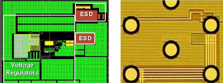
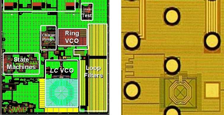
20 Die Photograph 388 µm 715 µm 20
21 Performance Summary Parameter Technology VCO Lock Range Ring-PLL LC -PLL GHz GHz RMS Jitter Mean ± 3 σ 975 ± 85 fs 536 ± 76 fs Phase Noise 45 nm SOI-CMOS (36 nm L gate ) At 1 MHz Offset dbc/hz dbc/hz At 10 MHz Offset dbc/hz dbc/hz Reference Spur At 100 MHz Offset 58.4 dbc 61.8 dbc Jitter Transfer Supply Consumption 3 db Bandwidth 6.6 MHz 6.6 MHz Peaking 0.41 db 0.54 db Current 28 ma 24 ma Voltage V (2.5 V nom) 21
22 Conclusion Designed dual-pll system for clocking multi-protocol wireline I/O in 45-nm SOI-CMOS processors Presented circuit and architectural techniques to minimize impact of PD-SOI floating-body and PVT variations Exceeded multi-protocol requirements GHz VCO lock range 975±85 fs rms jitter for ring-based PLL 535±76 fs rms jitter for LC-based PLL 22
23 Acknowledgments AMD Larry Bair John Faricelli Kurt Ireland Chad Lackey Jim Pattison Norma Rodriguez Keertika Singh Sam Sim GlobalFoundries Jung-Suk Goo Tilo Mantei René Nagel Lynne Okada Christoph Schwan Rasit Topaloglu Thomas Werner Jianhong Zhu Thank you for your attention! 23
Lecture 160 Examples of CDR Circuits in CMOS (09/04/03) Page 160-1
 Page 160-1") Lecture 160 Examples of CDR Circuits in CMOS (09/04/03) Page 160-1 LECTURE 160 CDR EXAMPLES INTRODUCTION Objective The objective of this presentation is: 1.) Show two examples of clock and data recovery
Lecture 160 Examples of CDR Circuits in CMOS (09/04/03) Page 160-1 LECTURE 160 CDR EXAMPLES INTRODUCTION Objective The objective of this presentation is: 1.) Show two examples of clock and data recovery
Lecture 23: PLLs. Office hour on Monday moved to 1-2pm and 3:30-4pm Final exam next Wednesday, in class
 EE241 - Spring 2013 Advanced Digital Integrated Circuits Lecture 23: PLLs Announcements Office hour on Monday moved to 1-2pm and 3:30-4pm Final exam next Wednesday, in class Open book open notes Project
ECEN689: Special Topics in High-Speed Links Circuits and Systems Spring 2010
 ECEN689: Special Topics in High-Speed Links Circuits and Systems Spring 010 Lecture 7: PLL Circuits Sam Palermo Analog & Mixed-Signal Center Texas A&M University Announcements Project Preliminary Report
Choosing Loop Bandwidth for PLLs
 Choosing Loop Bandwidth for PLLs Timothy Toroni SVA Signal Path Solutions April 2012 1 Phase Noise (dbc/hz) Choosing a PLL/VCO Optimized Loop Bandwidth Starting point for setting the loop bandwidth is
SiNANO-NEREID Workshop:
 SiNANO-NEREID Workshop: Towards a new NanoElectronics Roadmap for Europe Leuven, September 11 th, 2017 WP3/Task 3.2 Connectivity RF and mmw Design Outline Connectivity, what connectivity? High data rates
Fractional- N PLL with 90 Phase Shift Lock and Active Switched- Capacitor Loop Filter
 J. Park, F. Maloberti: "Fractional-N PLL with 90 Phase Shift Lock and Active Switched-Capacitor Loop Filter"; Proc. of the IEEE Custom Integrated Circuits Conference, CICC 2005, San Josè, 21 September
Signal Integrity Design of TSV-Based 3D IC
 Signal Integrity Design of TSV-Based 3D IC October 24, 21 Joungho Kim at KAIST joungho@ee.kaist.ac.kr http://tera.kaist.ac.kr 1 Contents 1) Driving Forces of TSV based 3D IC 2) Signal Integrity Issues
20 GHz Low Power QVCO and De-skew Techniques in 0.13µm Digital CMOS. Masum Hossain & Tony Chan Carusone University of Toronto
 20 GHz Low Power QVCO and De-skew Techniques in 0.13µm Digital CMOS Masum Hossain & Tony Chan Carusone University of Toronto masum@eecg.utoronto.ca Motivation Data Rx3 Rx2 D-FF D-FF Rx1 D-FF Clock Clock
High Performance Digital Fractional-N Frequency Synthesizers
 High Performance Digital Fractional-N Frequency Synthesizers Michael Perrott October 16, 2008 Copyright 2008 by Michael H. Perrott All rights reserved. Why Are Digital Phase-Locked Loops Interesting? PLLs
5.5: A 3.2 to 4GHz, 0.25µm CMOS Frequency Synthesizer for IEEE a/b/g WLAN
 5.5: A 3.2 to 4GHz, 0.25µm CMOS Frequency Synthesizer for IEEE 802.11a/b/g WLAN Manolis Terrovitis, Michael Mack, Kalwant Singh, and Masoud Zargari 1 Atheros Communications, Sunnyvale, California 1 Atheros
ECEN620: Network Theory Broadband Circuit Design Fall 2014
 ECEN60: Network Theory Broadband Circuit Design Fall 014 Lecture 13: Frequency Synthesizer Examples Sam Palermo Analog & Mixed-Signal Center Texas A&M University Agenda Frequency Synthesizer Examples Design
EE290C - Spring 2004 Advanced Topics in Circuit Design High-Speed Electrical Interfaces. Announcements
 EE290C - Spring 04 Advanced Topics in Circuit Design High-Speed Electrical Interfaces Lecture 11 Components Phase-Locked Loops Viterbi Decoder Borivoje Nikolic March 2, 04. Announcements Homework #2 due
Introduction to CMOS RF Integrated Circuits Design
 VI. Phase-Locked Loops VI-1 Outline Introduction Basic Feedback Loop Theory Circuit Implementation VI-2 What is a PLL? A PLL is a negative feedback system where an oscillatorgenerated signal is phase and
Multiple Reference Clock Generator
 A White Paper Presented by IPextreme Multiple Reference Clock Generator Digitial IP for Clock Synthesis August 2007 IPextreme, Inc. This paper explains the concept behind the Multiple Reference Clock Generator
Frequency Synthesizers for RF Transceivers. Domine Leenaerts Philips Research Labs.
 Frequency Synthesizers for RF Transceivers Domine Leenaerts Philips Research Labs. Purpose Overview of synthesizer architectures for RF transceivers Discuss the most challenging RF building blocks Technology
A 0.2-to-1.45GHz Subsampling Fractional-N All-Digital MDLL with Zero-Offset Aperture PD-Based Spur Cancellation and In-Situ Timing Mismatch Detection
 A 0.2-to-1.45GHz Subsampling Fractional-N All-Digital MDLL with Zero-Offset Aperture PD-Based Spur Cancellation and In-Situ Timing Mismatch Detection Somnath Kundu 1, Bongjin Kim 1,2, Chris H. Kim 1 1
A Dual-Step-Mixing ILFD using a Direct Injection Technique for High- Order Division Ratios in 60GHz Applications
 A Dual-Step-Mixing ILFD using a Direct Injection Technique for High- Order Division Ratios in 60GHz Applications Teerachot Siriburanon, Wei Deng, Ahmed Musa, Kenichi Okada, and Akira Matsuzawa Tokyo Institute
/$ IEEE
 IEEE TRANSACTIONS ON CIRCUITS AND SYSTEMS II: EXPRESS BRIEFS, VOL. 53, NO. 11, NOVEMBER 2006 1205 A Low-Phase Noise, Anti-Harmonic Programmable DLL Frequency Multiplier With Period Error Compensation for
DESIGN OF MULTIPLYING DELAY LOCKED LOOP FOR DIFFERENT MULTIPLYING FACTORS
 DESIGN OF MULTIPLYING DELAY LOCKED LOOP FOR DIFFERENT MULTIPLYING FACTORS Aman Chaudhary, Md. Imtiyaz Chowdhary, Rajib Kar Department of Electronics and Communication Engg. National Institute of Technology,
CHAPTER 6 PHASE LOCKED LOOP ARCHITECTURE FOR ADC
 138 CHAPTER 6 PHASE LOCKED LOOP ARCHITECTURE FOR ADC 6.1 INTRODUCTION The Clock generator is a circuit that produces the timing or the clock signal for the operation in sequential circuits. The circuit
26.8: A 1.9GHz Single-Chip CMOS PHS Cellphone
 26.8: A 1.9GHz Single-Chip CMOS PHS Cellphone William W. Si, Srenik Mehta, Hirad Samavati, Manolis Terrovitis, Michael Mack, KeithOnodera, SteveJen, Susan Luschas, Justin Hwang, SuniMendis, DavidSu, BruceWooley
Receiver Architecture
 Receiver Architecture Receiver basics Channel selection why not at RF? BPF first or LNA first? Direct digitization of RF signal Receiver architectures Sub-sampling receiver noise problem Heterodyne receiver
A Sub-0.75 RMS-Phase-Error Differentially-Tuned Fractional-N Synthesizer with On-Chip LDO Regulator and Analog-Enhanced AFC Technique
 A Sub-0.75 RMS-Phase-Error Differentially-Tuned Fractional-N Synthesizer with On-Chip LDO Regulator and Analog-Enhanced AFC Technique Lei Lu, Lingbu Meng, Liang Zou, Hao Min and Zhangwen Tang Fudan University,
A Wide-Bandwidth 2.4GHz ISM Band Fractional-N PLL with Adaptive Phase Noise Cancellation. Outline
 A Wide-Bandwidth 2.4GHz ISM Band Fractional-N PLL with Adaptive Phase Noise Cancellation Ashok Swaminathan,2, Kevin J. Wang, Ian Galton University of California, San Diego, CA 2 NextWave Broadband, San
A Modular All Digital PLL Architecture Enabling Both 1-to-2 GHz and 24-to 32-GHz Operation in 65nm CMOS
 A Modular All Digital PLL Architecture Enabling Both 1-to-2 GHz and 24-to 32-GHz Operation in 65nm CMOS A. V. Rylyakov 1, J. A. Tierno 1, D. Z. Turker 2, J.-O. Plouchart 1 H. A. Ainspan 1, D. J. Friedman
ISSCC 2003 / SESSION 20 / WIRELESS LOCAL AREA NETWORKING / PAPER 20.5
 ISSCC 2003 / SESSION 20 / WIRELESS LOCAL AREA NETWORKING / PAPER 20.5 20.5 A 2.4GHz CMOS Transceiver and Baseband Processor Chipset for 802.11b Wireless LAN Application George Chien, Weishi Feng, Yungping
A Low Phase Noise 24/77 GHz Dual-Band Sub-Sampling PLL for Automotive Radar Applications in 65 nm CMOS Technology
 A Low Phase Noise 24/77 GHz Dual-Band Sub-Sampling PLL for Automotive Radar Applications in 65 nm CMOS Technology Xiang Yi, Chirn Chye Boon, Junyi Sun, Nan Huang and Wei Meng Lim VIRTUS, Nanyang Technological
A 5GHz, 32mW CMOS Frequency Synthesizer with an Injection Locked Frequency Divider. Hamid Rategh, Hirad Samavati, Thomas Lee
 A 5GHz, 32mW CMOS Frequency Synthesizer with an Injection Locked Frequency Divider Hamid Rategh, Hirad Samavati, Thomas Lee OUTLINE motivation introduction synthesizer architecture synthesizer building
ECEN689: Special Topics in High-Speed Links Circuits and Systems Spring 2012
 ECEN689: Special Topics in High-Speed Links Circuits and Systems Spring 2012 Lecture 5: Termination, TX Driver, & Multiplexer Circuits Sam Palermo Analog & Mixed-Signal Center Texas A&M University Announcements
A CMOS Frequency Synthesizer with an Injection-Locked Frequency Divider for a 5 GHz Wireless LAN Receiver. Hamid Rategh
 A CMOS Frequency Synthesizer with an Injection-Locked Frequency Divider for a 5 GHz Wireless LAN Receiver Hamid Rategh Center for Integrated Systems Stanford University OUTLINE Motivation Introduction
Design Challenges In Multi-GHz PLL Frequency Synthesizers
 Design Challenges In Multi-GHz PLL Frequency Synthesizers Adrian Maxim Senior RF Design Engineer Silicon Laboratories Austin, TX, USA Email: acmaxim@yahoo.com OUTLINE PLL basics PLL second order effects
Enhancing FPGA-based Systems with Programmable Oscillators
 Enhancing FPGA-based Systems with Programmable Oscillators Jehangir Parvereshi, jparvereshi@sitime.com Sassan Tabatabaei, stabatabaei@sitime.com SiTime Corporation www.sitime.com 990 Almanor Ave., Sunnyvale,
A 2.4-GHz 24-dBm SOI CMOS Power Amplifier with Fully Integrated Output Balun and Switched Capacitors for Load Line Adaptation
 A 2.4-GHz 24-dBm SOI CMOS Power Amplifier with Fully Integrated Output Balun and Switched Capacitors for Load Line Adaptation Francesco Carrara 1, Calogero D. Presti 2,1, Fausto Pappalardo 1, and Giuseppe
DESIGN AND VERIFICATION OF ANALOG PHASE LOCKED LOOP CIRCUIT
 DESIGN AND VERIFICATION OF ANALOG PHASE LOCKED LOOP CIRCUIT PRADEEP G CHAGASHETTI Mr. H.V. RAVISH ARADHYA Department of E&C Department of E&C R.V.COLLEGE of ENGINEERING R.V.COLLEGE of ENGINEERING Bangalore
ISSCC 2006 / SESSION 33 / MOBILE TV / 33.4
 33.4 A Dual-Channel Direct-Conversion CMOS Receiver for Mobile Multimedia Broadcasting Vincenzo Peluso, Yang Xu, Peter Gazzerro, Yiwu Tang, Li Liu, Zhenbiao Li, Wei Xiong, Charles Persico Qualcomm, San
Hot Topics and Cool Ideas in Scaled CMOS Analog Design
 Engineering Insights 2006 Hot Topics and Cool Ideas in Scaled CMOS Analog Design C. Patrick Yue ECE, UCSB October 27, 2006 Slide 1 Our Research Focus High-speed analog and RF circuits Device modeling,
433MHz front-end with the SA601 or SA620
 433MHz front-end with the SA60 or SA620 AN9502 Author: Rob Bouwer ABSTRACT Although designed for GHz, the SA60 and SA620 can also be used in the 433MHz ISM band. The SA60 performs amplification of the
Low voltage LNA, mixer and VCO 1GHz
 DESCRIPTION The is a combined RF amplifier, VCO with tracking bandpass filter and mixer designed for high-performance low-power communication systems from 800-1200MHz. The low-noise preamplifier has a
A Low Area, Switched-Resistor Loop Filter Technique for Fractional-N Synthesizers Applied to a MEMS-based Programmable Oscillator
 A Low Area, Switched-Resistor Loop Filter Technique for Fractional-N Synthesizers Applied to a MEMS-based Programmable Oscillator ISSCC 00, Session 3. M.H. Perrott, S. Pamarti, E. Hoffman, F.S. Lee, S.
SG500. Low Jitter Spectrum Clock Generator for PowerPC Designs. Approved Product. FREQUENCY TABLE (MHz) PRODUCT FEATURES CONNECTION DIAGRAM
 PRODUCT FEATURES CONNECTION DIAGRAM") PRODUCT FEATURES Supports Power PC CPU s. Supports simultaneous PCI and Fast PCI Buses. Uses external buffer to reduce EMI and Jitter PCI synchronous clock. Fast PCI synchronous clock Separated 3.3 volt
PRODUCT FEATURES Supports Power PC CPU s. Supports simultaneous PCI and Fast PCI Buses. Uses external buffer to reduce EMI and Jitter PCI synchronous clock. Fast PCI synchronous clock Separated 3.3 volt
Low Power, Wide Bandwidth Phase Locked Loop Design
 Low Power, Wide Bandwidth Phase Locked Loop Design Hariprasath Venkatram and Taehwan Oh Abstract A low power wide bandwidth phase locked loop is presented in the paper. The phase frequency detector, charge
A Random and Systematic Jitter Suppressed DLL-Based Clock Generator with Effective Negative Feedback Loop
 A Random and Systematic Jitter Suppressed DLL-Based Clock Generator with Effective Negative Feedback Loop Seong-Jin An 1 and Young-Shig Choi 2 Department of Electronic Engineering, Pukyong National University
ISSCC 2003 / SESSION 20 / WIRELESS LOCAL AREA NETWORKING / PAPER 20.2
 ISSCC 2003 / SESSION 20 / WIRELESS LOCAL AREA NETWORKING / PAPER 20.2 20.2 A Digitally Calibrated 5.15-5.825GHz Transceiver for 802.11a Wireless LANs in 0.18µm CMOS I. Bouras 1, S. Bouras 1, T. Georgantas
A Review of Phase Locked Loop Design Using VLSI Technology for Wireless Communication.
 A Review of Phase Locked Loop Design Using VLSI Technology for Wireless Communication. PG student, M.E. (VLSI and Embedded system) G.H.Raisoni College of Engineering and Management, A nagar Abstract: The
Taheri: A 4-4.8GHz Adaptive Bandwidth, Adaptive Jitter Phase Locked Loop
 Engineering, Technology & Applied Science Research Vol. 7, No. 2, 2017, 1473-1477 1473 A 4-4.8GHz Adaptive Bandwidth, Adaptive Jitter Phase Locked Loop Hamidreza Esmaeili Taheri Department of Electronics
A Low-Noise Frequency Synthesizer for Infrastructure Applications
 A Low-Noise Frequency Synthesizer for Infrastructure Applications Shayan Farahvash, William Roberts, Jake Easter, Rachel Wei, Dave Stegmeir, Li Jin RFMD, USA Outline Motivation Design Challenges VCO Capacitor
A 2.4 GHz to 3.86 GHz digitally controlled oscillator with 18.5 khz frequency resolution using single PMOS varactor
 LETTER IEICE Electronics Express, Vol.9, No.24, 1842 1848 A 2.4 GHz to 3.86 GHz digitally controlled oscillator with 18.5 khz frequency resolution using single PMOS varactor Yangyang Niu, Wei Li a), Ning
A Low-Jitter Phase-Locked Loop Based on a Charge Pump Using a Current-Bypass Technique
 JOURNAL OF SEMICONDUCTOR TECHNOLOGY AND SCIENCE, VOL.14, NO.3, JUNE, 2014 http://dx.doi.org/10.5573/jsts.2014.14.3.331 A Low-Jitter Phase-Locked Loop Based on a Charge Pump Using a Current-Bypass Technique
Design of VCOs in Global Foundries 28 nm HPP CMOS
 Design of VCOs in Global Foundries 28 nm HPP CMOS Evan Jorgensen 33 rd Annual Microelectronics Conference Rochester Institute of Technology Department of Electrical and Microelectronic Engineering May
Design of Analog CMOS Integrated Circuits
 Design of Analog CMOS Integrated Circuits Behzad Razavi Professor of Electrical Engineering University of California, Los Angeles H Boston Burr Ridge, IL Dubuque, IA Madison, WI New York San Francisco
A Multiobjective Optimization based Fast and Robust Design Methodology for Low Power and Low Phase Noise Current Starved VCO Gaurav Sharma 1
 IJSRD - International Journal for Scientific Research & Development Vol. 2, Issue 01, 2014 ISSN (online): 2321-0613 A Multiobjective Optimization based Fast and Robust Design Methodology for Low Power
THE BASIC BUILDING BLOCKS OF 1.8 GHZ PLL
 THE BASIC BUILDING BLOCKS OF 1.8 GHZ PLL IN CMOS TECHNOLOGY L. Majer, M. Tomáška,V. Stopjaková, V. Nagy, and P. Malošek Department of Microelectronics, Slovak Technical University, Ilkovičova 3, Bratislava,
Noise Analysis of Phase Locked Loops
 Noise Analysis of Phase Locked Loops MUHAMMED A. IBRAHIM JALIL A. HAMADAMIN Electrical Engineering Department Engineering College Salahaddin University -Hawler ERBIL - IRAQ Abstract: - This paper analyzes
Phase Noise and Tuning Speed Optimization of a MHz Hybrid DDS-PLL Synthesizer with milli Hertz Resolution
 Phase Noise and Tuning Speed Optimization of a 5-500 MHz Hybrid DDS-PLL Synthesizer with milli Hertz Resolution BRECHT CLAERHOUT, JAN VANDEWEGE Department of Information Technology (INTEC) University of
A GHz Wideband Sub-harmonically Injection- Locked PLL with Adaptive Injection Timing Alignment Technique
 A 2.4 3.6-GHz Wideband Sub-harmonically Injection- Locked PLL with Adaptive Injection Timing Alignment Technique Abstract: This paper proposes a wideband sub harmonically injection-locked PLL (SILPLL)
Digital PWM IC Control Technology and Issues
 Digital PWM IC Control Technology and Issues Prof. Seth R. Sanders Angel V. Peterchev Jinwen Xiao Jianhui Zhang Department of EECS University of California, Berkeley Digital Control Advantages implement
Lecture 7: Components of Phase Locked Loop (PLL)
") Lecture 7: Components of Phase Locked Loop (PLL) CSCE 6933/5933 Instructor: Saraju P. Mohanty, Ph. D. NOTE: The figures, text etc included in slides are borrowed from various books, websites, authors pages,
Lecture 7: Components of Phase Locked Loop (PLL) CSCE 6933/5933 Instructor: Saraju P. Mohanty, Ph. D. NOTE: The figures, text etc included in slides are borrowed from various books, websites, authors pages,
Design of Low Noise 16-bit CMOS Digitally Controlled Oscillator
 Design of Low Noise 16-bit CMOS Digitally Controlled Oscillator Nitin Kumar #1, Manoj Kumar *2 # Ganga Institute of Technology & Management 1 nitinkumarvlsi@gmail.com * Guru Jambheshwar University of Science
A 20GHz Class-C VCO Using Noise Sensitivity Mitigation Technique
 Matsuzawa Lab. Matsuzawa & Okada Lab. Tokyo Institute of Technology A 20GHz Class-C VCO Using Noise Sensitivity Mitigation Technique Kento Kimura, Kenichi Okada and Akira Matsuzawa (WE2C-2) Matsuzawa &
1GHz low voltage LNA, mixer and VCO
 DESCRIPTION The is a combined RF amplifier, VCO with tracking bandpass filter and mixer designed for high-performance low-power communication systems from 800-1200MHz. The low-noise preamplifier has a
A CMOS Phase Locked Loop based PWM Generator using 90nm Technology Rajeev Pankaj Nelapati 1 B.K.Arun Teja 2 K.Sai Ravi Teja 3
 IJSRD - International Journal for Scientific Research & Development Vol. 3, Issue 06, 2015 ISSN (online): 2321-0613 A CMOS Phase Locked Loop based PWM Generator using 90nm Technology Rajeev Pankaj Nelapati
Package and Pin Assignment SSOP-6 (0.64mm pitch) OSCIN OSCOUT TXEN 3 VSS 4 TXOUT 5 VSS 6 7 MODIN 8 HiMARK SW DO RES RESB VREFP VSS Symbol
 OSCIN OSCOUT TXEN 3 VSS 4 TXOUT 5 VSS 6 7 MODIN 8 HiMARK SW DO RES RESB VREFP VSS Symbol") Low Power ASK Transmitter IC HiMARK Technology, Inc. reserves the right to change the product described in this datasheet. All information contained in this datasheet is subject to change without prior
Low Power ASK Transmitter IC HiMARK Technology, Inc. reserves the right to change the product described in this datasheet. All information contained in this datasheet is subject to change without prior
A VCO-based analog-to-digital converter with secondorder sigma-delta noise shaping
 A VCO-based analog-to-digital converter with secondorder sigma-delta noise shaping The MIT Faculty has made this article openly available. Please share how this access benefits you. Your story matters.
Jitter Measurements using Phase Noise Techniques
 Jitter Measurements using Phase Noise Techniques Agenda Jitter Review Time-Domain and Frequency-Domain Jitter Measurements Phase Noise Concept and Measurement Techniques Deriving Random and Deterministic
Analysis of Phase Noise Profile of a 1.1 GHz Phase-locked Loop
 Analysis of Phase Noise Profile of a 1.1 GHz Phase-locked Loop J. Handique, Member, IAENG and T. Bezboruah, Member, IAENG 1 Abstract We analyzed the phase noise of a 1.1 GHz phaselocked loop system for
<180 fs RMS Jitter 24-bit Step Size, Resolution 3 Hz typ Exact Frequency Mode Built in Digital Self Test 40 Lead 6x6 mm SMT Package: 36 mm 2
 Features RF Bandwidth: Maximum Phase Detector Rate 1 MHz Ultra Low Phase Noise -11 dbc/hz in Band Typ. Figure of Merit (FOM) -227 dbc/hz Typical Applications Cellular/4G, WiMax Infrastructure Repeaters
Integrated Circuit Design for High-Speed Frequency Synthesis
 Integrated Circuit Design for High-Speed Frequency Synthesis John Rogers Calvin Plett Foster Dai ARTECH H O US E BOSTON LONDON artechhouse.com Preface XI CHAPTER 1 Introduction 1 1.1 Introduction to Frequency
Radio-Frequency Conversion and Synthesis (for a 115mW GPS Receiver)
") Radio-Frequency Conversion and Synthesis (for a 115mW GPS Receiver) Arvin Shahani Stanford University Overview GPS Overview Frequency Conversion Frequency Synthesis Conclusion GPS Overview: Signal Structure
Radio-Frequency Conversion and Synthesis (for a 115mW GPS Receiver) Arvin Shahani Stanford University Overview GPS Overview Frequency Conversion Frequency Synthesis Conclusion GPS Overview: Signal Structure
A DPLL-based per Core Variable Frequency Clock Generator for an Eight-Core POWER7 Microprocessor
 A DPLL-based per Core Variable Frequency Clock Generator for an Eight-Core POWER7 Microprocessor José Tierno 1, A. Rylyakov 1, D. Friedman 1, A. Chen 2, A. Ciesla 2, T. Diemoz 2, G. English 2, D. Hui 2,
24-bit Step Size, Resolution 3 Hz typ Exact Frequency Mode Built-in Digital Self Test 40 Lead 6x6mm SMT Package: 36mm 2. Phased Array Applications
 FRACTIONAL-N PLL WITH INTEGRATED VCO, 80-80 MHz Features RF Bandwidth: 80 to 80 MHz Ultra Low Phase Noise -110 dbc/hz in Band Typ. Figure of Merit (FOM) -22 dbc < 180 fs RMS Jitter 24-bit Step Size, Resolution
PHASE-LOCKED loops (PLLs) are widely used in many
 are widely used in many") IEEE TRANSACTIONS ON CIRCUITS AND SYSTEMS II: EXPRESS BRIEFS, VOL. 58, NO. 3, MARCH 2011 149 Built-in Self-Calibration Circuit for Monotonic Digitally Controlled Oscillator Design in 65-nm CMOS Technology
IEEE TRANSACTIONS ON CIRCUITS AND SYSTEMS II: EXPRESS BRIEFS, VOL. 58, NO. 3, MARCH 2011 149 Built-in Self-Calibration Circuit for Monotonic Digitally Controlled Oscillator Design in 65-nm CMOS Technology
<180 fs RMS Jitter 24-bit Step Size, Resolution 3 Hz typ Exact Frequency Mode Built in Digital Self Test 40 Lead 6x6 mm SMT Package: 36 mm 2
 Features RF Bandwidth: Maximum Phase Detector Rate 1 MHz Ultra Low Phase Noise -11 dbc/hz in Band Typ. Figure of Merit (FOM) -227 dbc/hz Typical Applications Cellular/4G Infrastructure Repeaters and Femtocells
77 GHz VCO for Car Radar Systems T625_VCO2_W Preliminary Data Sheet
 77 GHz VCO for Car Radar Systems Preliminary Data Sheet Operating Frequency: 76-77 GHz Tuning Range > 1 GHz Output matched to 50 Ω Application in Car Radar Systems ESD: Electrostatic discharge sensitive
Radio Research Directions. Behzad Razavi Communication Circuits Laboratory Electrical Engineering Department University of California, Los Angeles
 Radio Research Directions Behzad Razavi Communication Circuits Laboratory Electrical Engineering Department University of California, Los Angeles Outline Introduction Millimeter-Wave Transceivers - Applications
I. INTRODUCTION. Architecture of PLL-based integer-n frequency synthesizer. TABLE I DIVISION RATIO AND FREQUENCY OF ALL CHANNELS, N =16, P =16
 320 IEEE TRANSACTIONS ON CIRCUITS AND SYSTEMS I: REGULAR PAPERS, VOL. 56, NO. 2, FEBRUARY 2009 A 5-GHz CMOS Frequency Synthesizer With an Injection-Locked Frequency Divider and Differential Switched Capacitors
An Analog Phase-Locked Loop
 1 An Analog Phase-Locked Loop Greg Flewelling ABSTRACT This report discusses the design, simulation, and layout of an Analog Phase-Locked Loop (APLL). The circuit consists of five major parts: A differential
A 10 bit, 1.8 GS/s Time Interleaved Pipeline ADC
 A 10 bit, 1.8 GS/s Time Interleaved Pipeline ADC M. Åberg 2, A. Rantala 2, V. Hakkarainen 1, M. Aho 1, J. Riikonen 1, D. Gomes Martin 2, K. Halonen 1 1 Electronic Circuit Design Laboratory Helsinki University
A 2.6GHz/5.2GHz CMOS Voltage-Controlled Oscillator*
 WP 23.6 A 2.6GHz/5.2GHz CMOS Voltage-Controlled Oscillator* Christopher Lam, Behzad Razavi University of California, Los Angeles, CA New wireless local area network (WLAN) standards have recently emerged
A Low-Jitter MHz DLL Based on a Simple PD and Common-Mode Voltage Level Corrected Differential Delay Elements
 Journal of Information Systems and Telecommunication, Vol. 2, No. 3, July-September 2014 166 A Low-Jitter 20-110MHz DLL Based on a Simple PD and Common-Mode Voltage Level Corrected Differential Delay Elements
Short Course On Phase-Locked Loops and Their Applications Day 5, AM Lecture. Advanced PLL Examples (Part I)
") Short Course On Phase-Locked Loops and Their Applications Day 5, AM Lecture Advanced PLL Examples (Part I) Michael Perrott August 15, 2008 Copyright 2008 by Michael H. Perrott All rights reserved. Outline
Short Course On Phase-Locked Loops and Their Applications Day 5, AM Lecture Advanced PLL Examples (Part I) Michael Perrott August 15, 2008 Copyright 2008 by Michael H. Perrott All rights reserved. Outline
Single-Ended to Differential Converter for Multiple-Stage Single-Ended Ring Oscillators
 IEEE JOURNAL OF SOLID-STATE CIRCUITS, VOL. 38, NO. 1, JANUARY 2003 141 Single-Ended to Differential Converter for Multiple-Stage Single-Ended Ring Oscillators Yuping Toh, Member, IEEE, and John A. McNeill,
A 4 µa-quiescent-current Dual- Mode Digitally-Controlled Buck Converter IC for Cellular Phone Applications
 A 4 µa-quiescent-current Dual- Mode Digitally-Controlled Buck Converter IC for Cellular Phone Applications Jinwen Xiao Angel Peterchev Jianhui Zhang Prof. Seth Sanders Power Electronics Group Dept. of
A Frequency Synthesis of All Digital Phase Locked Loop
 A Frequency Synthesis of All Digital Phase Locked Loop S.Saravanakumar 1, N.Kirthika 2 M.E.VLSI DESIGN Sri Ramakrishna Engineering College Coimbatore, Tamilnadu 1 s.saravanakumar21@gmail.com, 2 kirthi.com@gmail.com
A 60GHz Sub-Sampling PLL Using A Dual-Step-Mixing ILFD
 A 60GHz Sub-Sampling PLL Using A Dual-Step-Mixing ILFD Teerachot Siriburanon, Tomohiro Ueno, Kento Kimura, Satoshi Kondo, Wei Deng, Kenichi Okada, and Akira Matsuzawa Tokyo Institute of Technology, Japan
ECEN689: Special Topics in High-Speed Links Circuits and Systems Spring 2010
 ECEN689: Special Topics in High-Speed Links Circuits and Systems Spring 010 Lecture 3: CDR Wrap-Up Sam Palermo Analog & Mixed-Signal Center Texas A&M University Announcements Exam is April 30 Will emphasize
AST-GPSRF. GPS / Galileo RF Downconverter GENERAL DESCRIPTION FEATURES APPLICATIONS FUNCTIONAL BLOCK DIAGRAM. Preliminary Technical Data
 FEATURES Single chip GPS / Galileo downconverter GPS L1 band C/A code (1575.42 MHz) receiver GALILEO L1 band OS code (1575.42 MHz) receiver 2.7 V to 3.3 V power supply On-chip LNA On-chip PLL including
A 2.4 GHZ RECEIVER IN SILICON-ON-SAPPHIRE MICHAEL PETERS. B.S., Kansas State University, 2009 A REPORT
 A 2.4 GHZ RECEIVER IN SILICON-ON-SAPPHIRE by MICHAEL PETERS B.S., Kansas State University, 2009 A REPORT submitted in partial fulfillment of the requirements for the degree MASTER OF SCIENCE Department
Differential Amplifiers
 Differential Amplifiers Benefits of Differential Signal Processing The Benefits Become Apparent when Trying to get the Most Speed and/or Resolution out of a Design Avoid Grounding/Return Noise Problems
High Speed Communication Circuits and Systems Lecture 14 High Speed Frequency Dividers
 High Speed Communication Circuits and Systems Lecture 14 High Speed Frequency Dividers Michael H. Perrott March 19, 2004 Copyright 2004 by Michael H. Perrott All rights reserved. 1 High Speed Frequency
Improved Phase Noise Model. School of Electronics and Computer Science
 Improved Phase Noise Model for Ultra Wideband VCO Li Ke Reuben Wilcock Peter Wilson School of Electronics and Computer Science University of Southampton, UK Presentation outline Research motivation Improved
Extreme Temperature Invariant Circuitry Through Adaptive DC Body Biasing
 Extreme Temperature Invariant Circuitry Through Adaptive DC Body Biasing W. S. Pitts, V. S. Devasthali, J. Damiano, and P. D. Franzon North Carolina State University Raleigh, NC USA 7615 Email: wspitts@ncsu.edu,
Design and Implementation of High-Speed CMOS Clock and Data Recovery Circuit for Optical Interconnection Applications. Seong-Jun Song. Dec.
 MS Thesis esign and Implementation of High-Speed CMOS Clock and ata Recovery Circuit for Optical Interconnection Applications Seong-Jun Song ec. 20, 2002 oratory, epartment of Electrical Engineering and
CMOS 120 GHz Phase-Locked Loops Based on Two Different VCO Topologies
 JOURNAL OF ELECTROMAGNETIC ENGINEERING AND SCIENCE, VOL. 17, NO. 2, 98~104, APR. 2017 http://dx.doi.org/10.5515/jkiees.2017.17.2.98 ISSN 2234-8395 (Online) ISSN 2234-8409 (Print) CMOS 120 GHz Phase-Locked
A DESIGN EXPERIMENT FOR MEASUREMENT OF THE SPECTRAL CONTENT OF SUBSTRATE NOISE IN MIXED-SIGNAL INTEGRATED CIRCUITS
 A DESIGN EXPERIMENT FOR MEASUREMENT OF THE SPECTRAL CONTENT OF SUBSTRATE NOISE IN MIXED-SIGNAL INTEGRATED CIRCUITS Marc van Heijningen, John Compiet, Piet Wambacq, Stéphane Donnay and Ivo Bolsens IMEC
ECEN620: Network Theory Broadband Circuit Design Fall 2012
 ECEN620: Network Theory Broadband Circuit Design Fall 2012 Lecture 11: Charge Pump Circuits Sam Palermo Analog & Mixed-Signal Center Texas A&M University Announcements & Agenda Exam 1 is on Wed. Oct 3
24-bit Step Size, Resolution 3 Hz typ Exact Frequency Mode Built-in Digital Self Test 40 Lead 6x6mm SMT Package: 36mm 2. Phased Array Applications
 Features RF Bandwidth: 1815 to 2010 MHz Ultra Low Phase Noise -110 dbc/hz in Band Typ. Figure of Merit (FOM) -22 dbc < 180 fs RMS Jitter 24-bit Step Size, Resolution 3 Hz typ Exact Frequency Mode Built-in
A 1.9GHz Single-Chip CMOS PHS Cellphone
 A 1.9GHz Single-Chip CMOS PHS Cellphone IEEE JSSC, Vol. 41, No.12, December 2006 William Si, Srenik Mehta, Hirad Samavati, Manolis Terrovitis, Michael Mack, Keith Onodera, Steve Jen, Susan Luschas, Justin
A fully synthesizable injection-locked PLL with feedback current output DAC in 28 nm FDSOI
 LETTER IEICE Electronics Express, Vol.1, No.15, 1 11 A fully synthesizable injection-locked PLL with feedback current output DAC in 8 nm FDSOI Dongsheng Yang a), Wei Deng, Aravind Tharayil Narayanan, Rui
95GHz Receiver with Fundamental Frequency VCO and Static Frequency Divider in 65nm Digital CMOS
 95GHz Receiver with Fundamental Frequency VCO and Static Frequency Divider in 65nm Digital CMOS Ekaterina Laskin, Mehdi Khanpour, Ricardo Aroca, Keith W. Tang, Patrice Garcia 1, Sorin P. Voinigescu University
A Phase-Locked Loop with Embedded Analog-to-Digital Converter for Digital Control
 A Phase-Locked Loop with Embedded Analog-to-Digital Converter for Digital Control Sooho Cha, Chunseok Jeong, and Changsik Yoo A phase-locked loop (PLL) is described which is operable from 0.4 GHz to 1.2