S. Square Enterprise Company Limited Pro-Wave Electronics Corporation
|
|
|
- Ralf Parks
- 5 years ago
- Views:
Transcription

1 SSOP20 Features: Operating Voltage: 6 12Vdc single source Operating Frequency: broadband output ranging up to 200KHz Variable R/C Oscillator: compensates for transducer resonate frequency drift due to temperature. High Gain Amplifier: varies with time over 32 steps Integrated Band Pass Filter: reduces external component count Bi-direction I/O Pin: simplifies the control function for transmitting a pulse and receiving an echo An adjustable System Clock: enables the control of, the number of pulses transmitted, the slope of the variable gain amplifier, and the pulse repetition rate. The IC is suitable for use in car reversing aids, electronic tape measures and other sonar ranging applications. Description: The PW-0268 ultrasonic sonar ranging IC is ideally suited for echo ranging systems. This chip has many design features to enhance its performance and ease of use in this application. The externally tunable RC Oscillator automatically tracks and compensates for the shift of the resonate frequency of the transducer due to temperature changes. The Fix Gain Preamplifier can be tailored to compensate for varying transducer sensitivities. The 32-step Time Controlled Variable Gain Amplifier slope can be modified by adjusting the frequency of the system clock. An onboard Comparator converts the analog signal of the returning echo to a TTL level digital signal for use with an external microprocessor. The integrated Band Pass Filters can be adjusted for custom applications by changing a few external components. The frequency of the System Clock can be adjusted to control other operating parameters of the chip including the transmit pulse width and sample rate. The I_O pin, (pin 1) is a bi-direction pin and is designed as an open collector connection with an internal pull high resistor. When the I_O pin is being pulled low by an external transistor, the RC oscillator generates a tone burst signal at DRIVER_0 (pin 11), the output driver stage for the transducer. After the transmit pulse, the I_O pin, (pin 1) will again go low if a valid echo signal is detected. The reflected echo signal is presented to the first stage pre-amplifier through ECHO (pin 10). The gain of preamplifier can be adjusted to accommodate transducers with varying sensitivities by changing an external resistor between ECHO (pin 10) and GR_I (pin 9). The 32 steps time controlled variable gain amplifier input TCG_I (pin7) and output TCG_O (pin 6) is synchronized to start incrementing at the end of control pulse signal I-O, (pin 1) and is reset at the beginning of the next control pulse. Only a few passive components are needed for the active band pass filter. There are two stages, a low pass, LP_I (pin 5) and LP_O (pin 4) and upper band pass, HP_I (pin 3) to HP_O (pin 2). The center frequency and bandwidth of the filter are chosen based on the type of ultrasonic transducer being used and the specific application. The amplified echo signal after being filtered is routed to a comparator, which shapes and coverts the analog echo signal into digital signal outputted at I_O (pin 1) for further µp handling. The unique temperature compensating Ultrasonic R/C Oscillator circuitry tracks the resonant frequency drift of the transducer that is causes by environment temperature changes. Simply adding dual diodes and one resistor between DRIVER_O (pin 11) and Ftrace (pin 12) is all that is needed to complete this function. 1 of 12
2 Block Diagram: Vref Vcc Vreg GND CLK ORC3 ORC2 ORC1 Ftrace Driver_O V Regulator System Clock Ultrasonic R/C Oscillator Sensor Driver Timer Auto Frequency Tracking High-Speed Comparator Control Center Band-pass Filter 32 Steps TCG Amp Fixed Gain Amp 1st Pre-Amp I_O HP_O HP_I LP_O LP_I TCG_O TCG_I GR_O GR_I ECHO Pin Assignment: I_O HP_O HP_I LP_O LP_I TCG_O TCG_I GR_O GR_I ECHO Vref Vcc Vreg GND CLK ORC3 ORC2 ORC1 Ftrace Driver_O 2 of 12
3 Specifications: Unless otherwise specified, all data measured under Vcc = 9V, F = 40KHz,Temperature =25 C Parameter Symbol Condition Min. Typ. Max. Unit Supply Voltage Vcc Vreg = 4V 6 12 V Supply Current Icc Vcc = 6 ~ 12V ma Regulated Voltage Vreg Vcc = 6 ~ 12V V Reference Voltage Vref Vcc = 6 ~12V, RL>2KΩ V Op-Amp Slew Rate SR Vin = 3Vpp V/μs Comparator Trigger Level Tcomp Over Vref mv System Clock Frequency CLKf R=39KΩ,C=22pF KHz System Clock Frequency Range CLKr KHz Ultrasonic Oscillation Frequency Foscf R=3.9KΩ,C=2200pF KHz Ultrasonic Oscillation Frequency Range Foscr KHz 2 nd Amp Gain GR db Time Controlled Gain Amplifier TCGain Min(1x, 0dB) Max(58x, 35.2dB) db Bandwidth of 2nd Amp GRbw Gain = 30dB KHz Driving Current MCU Input Level MCU Output Level Idrv Voh=Vreg-0.7V Isink Vol=0.7v-GND MCUVIH MCUVIL MCUVOH MCUVOL ma V Vcc MCU Low Level Input Current MCUIOL ma I_O Internal Pull Up Resistance Rup KΩ Absolute Maximum Ratings Description Symbol Condition Min. Max. Unit Supply Voltage Vcc 0 15 V Operation Temperature Topr Storage Temperature Tstg Max. Pin Input Voltage Vimax I_O, Vcc -0.3 Vcc+0.3 Others -0.3 Vreg+0.3 Max. Input Current Iimax * ma *To prevent latch up, the instantaneous input current should be no large than 100mA for each pins. V 3 of 12
4 Pins Description: Pin Name Description Pin Name Description 1 I_O Input/Output 11 Driver_O Transducer driving output 2 HP_O High pass filter output 12 Ftrace Frequency tracing input 3 HP_I High pass filter input 13 ORC1 RC oscillator: terminal 1 4 LP_O Low pass filter output 14 ORC2 RC oscillator: terminal 2 5 LP_I Low pass filter input 15 ORC3 RC oscillator: terminal 3 6 TCG_O Time controlled gain output 16 CLK System clock 7 TCG_I Time controlled gain input 17 GND Ground 8 GR_O External adjustable gain output 18 Vreg Regulated voltage for internal analogue devices 9 GR_I External adjustable gain input 19 Vcc Power supply 10 ECHO Receiving echo input 20 Vref Reference voltage output Application Circuit: for car reversing aids (values should be changed for other applications) 4 of 12
5 Application Note The circuit shown on page 4 is a typical circuit for car reversing aids. The RC Oscillator generates a tone burst when a low level pulse is applied to the I_O pin, (pin 1). To accommodate tolerance variations of transducers during manufacturing, a 1K-ohm variable resistor (R1) is provided to trim the output operating frequency. The range of adjustment is from KHz. and allows for a better match of the drive signal to the resonate frequency of the transducer. The active burst number (number of pulses transmitted) is controlled by the pulse width of the low level signal applied to the I_O pin, (pin 1). The tone burst output, Driver_O (pin 11), drives the transducer through a MOSFET transistor and impedance matching transformer IFT. The inductance in the secondary winding of the transformer is designed to tune out the reactance of the parallel capacitance of the transducer. The high output voltage of the tone burst is snubbed by two diodes and the returning echo signal is passed on to the first stage pre-amplifier. The signal is then passed on to the second stage fix gain amplifier and finally to the third stage 32-step time controlled variable gain amplifier. The gain of the pre-amplifier should be properly set to meet the sensitivity needs of the transducer and application requirements. The center frequency of band-pass filter should be chosen to exactly match the frequency of the RC Oscillator and considerations for the width of pass-band filter should be made based on actual application requirements. If the amplified echo signal from the output of the band pass filter exceeds 0.35V + Vref, the comparator will output a low pulse to the I_O pin, (pin 1). The width of the low level pulse is proportional to the echo signal strength. 5 of 12
6 The above description is summarized in the signal timing charts illustrated below. MCU output: H: 1ms/Div., V: 2.0V/Div. The RC oscillator will be enabled in the duration of input pulse. The maximum pulse width is 400/F and any time longer than this upper limit will be ignored. Driver_O (Pin 11): H: 1ms/Div., V: 2.0V/Div. The next input pulse will be ignored if the pulse repetition rate is shorter than 10000/F + pulse width. F : Frequency of system clock Transducer Oscillation: H: 1ms/Div., V: 50V/Div. HP_O (Pin 2): H: 1ms/Div., V: 2.0V/Div. Output at Pin 1 I_O: H: 1ms/Div., V: 5.0V/Div. 6 of 12
7 The resonate frequency of ultrasonic piezo transducers varies in an inversely proportional relationship to temperature. The lower the temperature, the higher the resonate frequency, the higher the temperature the lower the resonate frequency. This property of piezo transducers may cause a mismatch between transducer and drive signal with changes in ambient temperature and reduces efficiency of the system when the frequency of the drive circuit remains constant and does not track the resonate frequency shift of the transducer. Therefore it is desirable to have the output frequency of the drive source track the resonate frequency of the transducer with changes in ambient temperature. The Auto Frequency Tracking circuitry between Ftrace, (pin 12), and Drive_O, (pin 11) is used to accomplish this task. The voltage change at Ftrace (pin 11) varies in proportion to the forward bias voltage change across diodes D1, D2. This change is caused by the negative temperature coefficient of the diodes and the ratio of the resistor circuit R2/R3. A lower temperature increases the voltage drop across the diodes. This intern accelerates the charge rate of an internal integrator circuit controlling the R/C Oscillator, ORC3, (pin15). The net result is the adjustment to the R/C Oscillator increases the resonate frequency of the output, Drive_O, (pin11). Conversely, a higher temperature decreases the voltage drop across the diodes. This slows the charge rate of the internal integrator circuit controlling the R/C Oscillator. The net result of this adjustment is to decrease the resonate frequency of the output Drive_O, (pin 11). Choose values for the components R1, R2, R3 and C1 that will best track the characteristic resonate frequency shift curves due to temperature for a specific transducer. Recommended values for the following transducers are listed below. Used Transducer R1(Ohm) R2(Ohm) R3(Ohm) C1(pF) 400EP14D SR GE For a fixed output of 40KHz at Drive_O (pin 11) simply remove D1, D2 and R2 and set R1 = 4,500 Ohm, C1 = 2,200 pf, and R3 = 510 Ohm. The system clock CLK (pin 16) controls the maximum input pulse width, the slope of time controlled gain amplifier and pulse repetition rate. For example, as illustrated in the block diagram, if the system clock is set to 660KHz (C2: 22pF, R4: 39K Ohm), then: (1) The maximum input pulse width is 400/F = 400/660K = 0.6 ms and any duration longer than 0.6ms will be ignored. (2) The step duration of the 32 step time controlled gain amplifier is equal to 220/F = ms, starting from the end of the pulse on the I_O pin, (pin 1). (3) The minimum pulse repetition rate is 10000/F + pulse width = 10000/F ms (20 bursts of 40KHz) = 10000/660K = ms. For long distance measurements of 18 meters (one way distance), the system clock should be set as follows: Min. Pulse Repetition Rate = 10000/F = 167 ms (30 bursts of 40KHz) Frequency of System Clock F = 60 Khz For additional information about an 18-meter tape measure circuit, please consult with the factory. 7 of 12
8 Time Controlled Gain Amplifier: Gain (db) Steps The time controlled gain amplifier is stepping up once the input pulse falling. The time duration can be calculated as: T = 220/F F: Frequency of System Clock 8 of 12
 9 of")
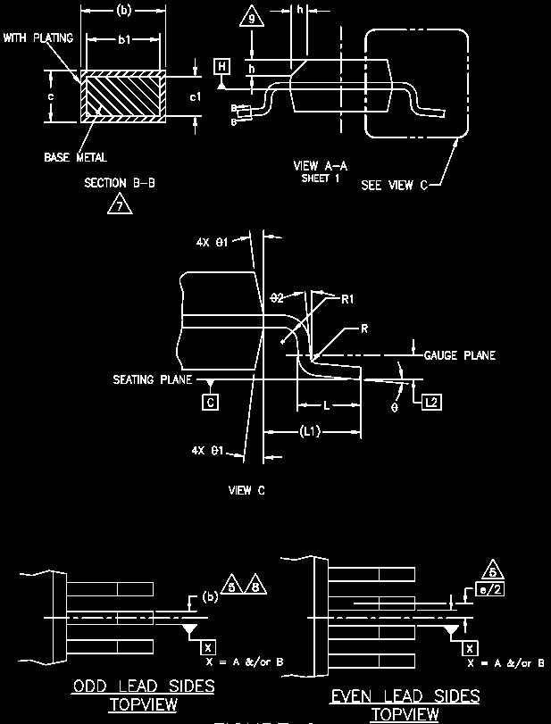
9 Package and Dimensions: 20 Pins, SSOP (150mil) 9 of 12
10 10 of 12
11 Symbol Min. Nom. Max. A A A b b c c D BSC E BSC E BSC e BAS L L REF L BAS R R aaa bbb ccc ddd eee of 12
12 Notes: Dimensioning and tolerancing per ANSI Y14.5M Dimensions in inches (angles in degrees) Dimension D does not include mold flash, protrusions or gate burrs. Mold flash, protrusions or gate burrs shall not exceed per end. Dimension E1 does not include interlead flash or protrusions. Interlead flash or protrusions shall not exceed per side. D1 and E1 dimensions are determined at datum H. The package top may be smaller than the package bottom. Dimensions D and E1 are determined at the outermost extremes of the plastic body exclusive of mold flash, tie bar burrs, gate burrs and interlead flash, but including any mismatch between the top and bottom of the plastic. Datum A and B to be determined at datum H. N is the maximum number of terminal position. (N=20) The dimensions apply to the flat section of the lead between to inches from the lead tip. Dimension b does not include dambar protrusion. Allowable dambar protrusion shall be total in excess of b dimension at maximum material condition. The dambar can not be located on the lower radius of the foot. Refer to JEDEC MO-137 variation AD. JEDEC is the registered trademark of JEDEC SOLID STATE TECHNOLOGY ASSOCIATION Copyright 2004 Pro-Wave Electronics Corp. 9/15/ of 12
Low On-Resistance Wideband/Video Quad 2-Channel Mux/DeMux
 DESCRIPTION The is a true bidirectional Quad 2-channel multiplexer/ de-multiplexer utilizing CMOS Technology. It is recommended for both RGB and composite video switching applications. The video switch
Low Power 315/433 MHz OOK/ASK Superheterodyne PT4316 Receiver with SAW-based Oscillator DESCRIPTION
 Low Power 315/433 MHz OOK/ASK Superheterodyne DESCRIPTION The is a very low power consumption single chip OOK/ASK superheterodyne receiver for the 315MHz and 434MHz frequency bands and which offers a high
4-Channel Input Audio Processor
 DESCRIPTION is a four-channel input digital audio processor utilizing CMOS Technology. Volume, Bass, Treble and Balance are incorporated into a single chip. Loudness Function and Selectable Input Gain
Remote Control Encoder
 DESCRIPTION is a remote control encoder utilizing CMOS Technology specially designed for use with the PT2128. Using a special coding technique, increases noise immunity to a very great extent. It is housed
Princeton Technology Corp.
 DESCRIPTION PT2258 is a 6-Channel Electronic Volume Controller IC utilizing CMOS Technology specially designed for the new generation of AV Multi-Channel Audio System. PT2258 provides an I 2 C Control
Remote Control Encoder IC
 DESCRIPTION is a remote control encoder paired with PT2294 utilizing CMOS Technology. It encodes data and address pins into a serial coded waveform suitable for RF modulation. has a maximum of 12-bit of
2-Channel Audio Processor IC
 DESCRIPTION is a two-channel digital audio processor utilizing CMOS Technology. Volume, Bass, Treble and Balance Controls are incorporated into a single chip. Loudness Function is also provided to build
6-Ch Audio Selector PT2323
 DESCRIPTION is a 6-Channel Audio Selector utilizing CMOS Technology specially designed for Home Theater System. It provides a built-in 2-Channel to 6-Channel Translator, which can directly mix traditional
HA Features. 12MHz, High Input Impedance, Operational Amplifier. Applications. Pinout. Part Number Information. Data Sheet May 2003 FN2893.
 OBSOLETE PRODUCT POSSIBLE SUBSTITUTE PRODUCT HA-2525 HA-2515 Data Sheet May 23 FN2893.5 12MHz, High Input Impedance, Operational Amplifier HA-2515 is a high performance operational amplifier which sets
2W 2 Class AB Audio Power Amplifier
 DESCRIPTION The is a power amplifier utilizing CMOS Technology specially designed for audio purpose. It can deliver 2W 2 power output to the 5V power voltage. The power consumption is very low in stand-by.
1/3 Duty General Purpose LCD Driver IC PT6523
 DESCRIPTION PT6523 is an LCD Driver IC which can drive up to 156 segments. It can be used for frequency display in microprocessor-controlled radio receiver and in other display applications. PT6523 supports
DATASHEET HA Features. Applications. Pinout. Part Number Information. 12MHz, High Input Impedance, Operational Amplifier
 12MHz, High Input Impedance, Operational Amplifier OBSOLETE PRODUCT POSSIBLE SUBSTITUTE PRODUCT HA-2525 DATASHEET FN289 Rev 6. HA-255 is an operational amplifier whose design is optimized to deliver excellent
DATASHEET HFA1112. Features. Applications. Related Literature. Pin Descriptions. Ordering Information
 DATASHEET HFA1112 85MHz, Low Distortion Programmable Gain Buffer Amplifiers FN2992 Rev 8. July 27, 25 The HFA1112 is a closed loop Buffer featuring user programmable gain and ultra high speed performance.
P SUFFIX CASE 646 Single Supply Split Supplies SO-14 D SUFFIX CASE 751A PIN CONNECTIONS
 Dual Operational Amplifier and Dual Comparator The MC05 contains two differential-input operational amplifiers and two comparators, each set capable of single supply operation. This operational amplifier-comparator
RV4141A Low-Power, Ground-Fault Interrupter
 RV4141A Low-Power, Ground-Fault Interrupter Features Powered from the AC Line Built-In Rectifier Direct Interface to SCR 500μA Quiescent Current Precision Sense Amplifier Adjustable Time Delay Minimum
SR A, 30V, 420KHz Step-Down Converter DESCRIPTION FEATURES APPLICATIONS TYPICAL APPLICATION
 SR2026 5A, 30V, 420KHz Step-Down Converter DESCRIPTION The SR2026 is a monolithic step-down switch mode converter with a built in internal power MOSFET. It achieves 5A continuous output current over a
HA Features. Quad, 3.5MHz, Operational Amplifier. Applications. Pinout. Ordering Information. Data Sheet July 2004 FN2922.5
 HA-4741 Data Sheet July 24 FN2922. Quad, 3.MHz, Operational Amplifier HA-4741, which contains four amplifiers on a monolithic chip, provides a new measure of performance for general purpose operational
MP A, 36V, 700KHz Step-Down Converter with Programmable Output Current Limit
 The Future of Analog IC Technology MP2490 1.5A, 36V, 700KHz Step-Down Converter with Programmable Output Current Limit DESCRIPTION The MP2490 is a monolithic step-down switch mode converter with a programmable
HA Features. 400MHz, Fast Settling Operational Amplifier. Applications. Ordering Information. Pinout. Data Sheet August 2002 FN2897.
 HA-5 Data Sheet August FN97. MHz, Fast Settling Operational Amplifier The Intersil HA-5 is a wideband, very high slew rate, monolithic operational amplifier featuring superior speed and bandwidth characteristics.
MP2494 2A, 55V, 100kHz Step-Down Converter
 The Future of Analog IC Technology MP2494 2A, 55V, 100kHz Step-Down Converter DESCRIPTION The MP2494 is a monolithic step-down switch mode converter. It achieves 2A continuous output current over a wide
Dual Channel PWM Controller with SCP / DTC Function
 Dual Channel PWM Controller with SCP / DTC Function General Description The FP545A is a dual channel PWM buck controller with short circuit protection (SCP) and adjustable maximum duty control (DTC) function.
HIP V, 300mA Three Phase High Side Driver. Features. Applications. Ordering Information. Pinout. July 2004
 HIP0 Data Sheet July 00 FN. 0V, 00mA Three Phase High Side Driver The HIP0 is a three phase high side N-channel MOSFET driver, specifically targeted for PWM motor control. Two HIP0 may be used together
NGD8201AN - 20 A, 400 V, N-Channel Ignition IGBT, DPAK
 NGD8201AN - 20 A, 400 V, N-Channel, DPAK Pb Description This Logic Level Insulated Gate Bipolar Transistor (IGBT) features monolithic circuitry integrating ESD and Over Voltage clamped protection for use
DATASHEET HA Features. Applications. Pinout. Ordering Information. Quad, 3.5MHz, Operational Amplifier. FN2922 Rev 5.00 Page 1 of 8.
 DATASHEET HA-4741 Quad, 3.5MHz, Operational Amplifier HA-4741, which contains four amplifiers on a monolithic chip, provides a new measure of performance for general purpose operational amplifiers. Each
MC33064DM 5 UNDERVOLTAGE SENSING CIRCUIT
 Order this document by MC3464/D The MC3464 is an undervoltage sensing circuit specifically designed for use as a reset controller in microprocessor-based systems. It offers the designer an economical solution
Green-Mode PWM Controller with Hiccup Protection
 Green-Mode PWM Controller with Hiccup Protection Features Current Mode Control Standby Power below 100mW Under-Voltage Lockout (UVLO) Non-Audible-Noise Green-Mode Control 65KHz Switching Frequency Internal
Green-Mode PWM Controller with Hiccup Protection
 Green-Mode PWM Controller with Hiccup Protection Features Current Mode Control Standby Power below 100mW Under-Voltage Lockout (UVLO) Non-Audible-Noise Green-Mode Control 65KHz Switching Frequency Internal
Remote Control Decoder IC
 V1.2-1 - April, 2006 查询 供应商 捷多邦, 专业 PCB 打样工厂,24 小时加急出货 DESCRIPTION is a remote control decoder paired with PT2264 utilizing CMOS Technology. It has 12 bits of tri-state address pins providing a maximum
DATASHEET CA Applications. Pinout. Ordering Information. General Purpose NPN Transistor Array. FN483 Rev.6.00 Page 1 of 7.
 DATASHEET CA-386 General Purpose NPN Transistor Array The CA386 consists of five general-purpose silicon NPN transistors on a common monolithic substrate. Two of the transistors are internally connected
TEMP. PKG. -IN 1 16 S/H CONTROL PART NUMBER RANGE
 DATASHEET 7ns, Low Distortion, Precision Sample and Hold Amplifier FN59 Rev 5. The combines the advantages of two sample/ hold architectures to create a new generation of monolithic sample/hold. High amplitude,
LF442 Dual Low Power JFET Input Operational Amplifier
 LF442 Dual Low Power JFET Input Operational Amplifier General Description The LF442 dual low power operational amplifiers provide many of the same AC characteristics as the industry standard LM1458 while
LF147 - LF247 LF347 WIDE BANDWIDTH QUAD J-FET OPERATIONAL AMPLIFIERS
 LF147 - LF247 LF347 WIDE BANDWIDTH QUAD J-FET OPERATIONAL AMPLIFIERS LOW POWER CONSUMPTION WIDE COMMON-MODE (UP TO V + CC ) AND DIFFERENTIAL VOLTAGE RANGE LOW INPUT BIAS AND OFFSET CURRENT OUTPUT SHORT-CIRCUIT
NGD18N40ACLB - 18 A, 400 V, N-Channel Ignition IGBT, DPAK
 NGD18N40ACLB - 18 A, 400 V, N-Channel Ignition IGBT, DPAK Pb Description This Logic Level Insulated Gate Bipolar Transistor (IGBT) features monolithic circuitry integrating ESD and Over Voltage clamped
HA, HA Absolute Maximum Ratings Supply Voltage Between V+ and V Terminals V Differential Input Voltage V
 HA, HA Data Sheet October 6, FN9.9 Dual and Quad, 8MHz, Low Noise Operational Amplifiers Low noise and high performance are key words describing HA and HA. These general purpose amplifiers offer an array
RC4136 General Performance Quad 741 Operational Amplifier
 RC General Performance Quad 7 Operational Amplifier www.fairchildsemi.com Features Unity gain bandwidth MHz Short circuit protection No frequency compensation required No latch-up Large common mode and
8-Bit, high-speed, µp-compatible A/D converter with track/hold function ADC0820
 8-Bit, high-speed, µp-compatible A/D converter with DESCRIPTION By using a half-flash conversion technique, the 8-bit CMOS A/D offers a 1.5µs conversion time while dissipating a maximum 75mW of power.
HIGH SPEED, 100V, SELF OSCILLATING 50% DUTY CYCLE, HALF-BRIDGE DRIVER
 Data Sheet No. 60206 HIGH SPEED, 100V, SELF OSCILLATING 50% DUTY CYCLE, HALF-BRIDGE DRIVER Features Simple primary side control solution to enable half-bridge DC-Bus Converters for 48V distributed systems
ThermalMax. Obsolete PRODUCT HIGHLIGHT PACKAGE ORDER INFO. 0 to 70 LX1810-CDB
 DESCRIPTION The is a Full-Bridge thermo-electric cooler (TEC) controller specifically designed for high performance opto-electronic products where precise temperature control is required. These products
DATASHEET X Features. Pinout. Ordering Information. Dual Digitally Controlled Potentiometers (XDCPs ) FN8186 Rev 1.
 FN8186 Rev 1.") DATASHEET X93254 Dual Digitally Controlled Potentiometers (XDCPs ) The Intersil X93254 is a dual digitally controlled potentiometer (XDCP). The device consists of two resistor arrays, wiper switches, a
DATASHEET X93254 Dual Digitally Controlled Potentiometers (XDCPs ) The Intersil X93254 is a dual digitally controlled potentiometer (XDCP). The device consists of two resistor arrays, wiper switches, a
RV4145A. Low Power Ground Fault Interrupter. Features. Description. Block Diagram.
 Low Power Ground Fault Interrupter www.fairchildsemi.com Features No potentiomenter required Direct interface to SCR Supply voltage derived from AC line 26V shunt Adjustable sensitivity Grounded neutral
Green-Mode PWM Controller with Hiccup Protection
 Green-Mode PWM Controller with Hiccup Protection Features Current mode control Standby power below 100mW Under-voltage lockout (UVLO) Non-audible-noise green-mode control 100KHz switching frequency Internal
ML12002 Analog Mixer. There are two package offerings: Plastic Dual Inline 14 Lead, P Dip. Plastic Surface Mount 14 Lead SOIC.
 Analog Mixer Legacy Device: Motorola MC00 The ML00 is a double balanced analog mixer, including an input amplifier feeding the mixer carrier port and a temperature compensated bias regulator. The input
CA3096, CA3096A, CA3096C
 January OBSOLETE PRODUCT POSSIBLE SUBSTITUTE PRODUCT HFA39 CA39, CA39A, CA39C NPN/PNP Transistor Arrays Applications Five-Independent Transistors - Three NPN and - Two PNP Differential Amplifiers DC Amplifiers
DATASHEET X Features. Pinout. Ordering Information. Dual Digitally Controlled Potentiometers (XDCPs ) FN8187 Rev 1.
 FN8187 Rev 1.") DATASHEET X93255 Dual Digitally Controlled Potentiometers (XDCPs ) The Intersil X93255 is a dual digitally controlled potentiometer (XDCP). The device consists of two resistor arrays, wiper switches, a
DATASHEET X93255 Dual Digitally Controlled Potentiometers (XDCPs ) The Intersil X93255 is a dual digitally controlled potentiometer (XDCP). The device consists of two resistor arrays, wiper switches, a
HA-2520, HA-2522, HA-2525
 HA-, HA-, HA- Data Sheet November, 6 FN894.8 MHz, High Slew Rate, Uncompensated, High Input Impedance, Operational Amplifiers HA-, HA-, HA- comprise a series of operational amplifiers delivering an unsurpassed
DATASHEET CA3096, CA3096A, CA3096C. Description. Applications. CA3096, CA3096A, CA3096C Essential Differences. Part Number Information.
 DATASHEET CA39, CA39A, CA39C NPN/PNP Transistor Arrays Applications Five-Independent Transistors - Three NPN and - Two PNP Differential Amplifiers DC Amplifiers Sense Amplifiers Level Shifters Timers Lamp
TLC5620C, TLC5620I QUADRUPLE 8-BIT DIGITAL-TO-ANALOG CONVERTERS
 Four -Bit Voltage Output DACs 5-V Single-Supply Operation Serial Interface High-Impedance Reference Inputs Programmable or 2 Times Output Range Simultaneous-Update Facility Internal Power-On Reset Low
Green-Mode PWM Controller with Integrated Protections
 Green-Mode PWM Controller with Integrated Protections Features Current mode PWM Very low startup current Under-voltage lockout (UVLO) Non-audible-noise green-mode control Programmable switching frequency
Thermocouple Conditioner and Setpoint Controller AD596*/AD597*
 a FEATURES Low Cost Operates with Type J (AD596) or Type K (AD597) Thermocouples Built-In Ice Point Compensation Temperature Proportional Operation 10 mv/ C Temperature Setpoint Operation ON/OFF Programmable
SP723 Lead-Free/Green
 TVS Diode Arrays The SP73 is an array of SCR/Diode bipolar structures for ESD and over-voltage protection of sensitive input circuits. The SP73 has protection SCR/Diode device structures per input. There
AD596/AD597 SPECIFICATIONS +60 C and V S = 10 V, Type J (AD596), Type K (AD597) Thermocouple,
, Type K (AD597) Thermocouple,") AD597 SPECIFICATIONS (@ +60 C and V S = 10 V, Type J (AD596), Type K (AD597) Thermocouple, unless otherwise noted) Model AD596AH AD597AH AD597AR Min Typ Max Min Typ Max Min Typ Max Units ABSOLUTE MAXIMUM
AD597 SPECIFICATIONS (@ +60 C and V S = 10 V, Type J (AD596), Type K (AD597) Thermocouple, unless otherwise noted) Model AD596AH AD597AH AD597AR Min Typ Max Min Typ Max Min Typ Max Units ABSOLUTE MAXIMUM
HA5023. Dual 125MHz Video Current Feedback Amplifier. Features. Applications. Ordering Information. Pinout. Data Sheet September 30, 2015 FN3393.
 HA523 Data Sheet September 3, 215 FN3393.9 Dual 125MHz Video Current Feedback Amplifier The HA523 is a wide bandwidth high slew rate dual amplifier optimized for video applications and gains between 1
AIC1340 High Performance, Triple-Output, Auto- Tracking Combo Controller
 High Performance, Triple-Output, Auto- Tracking Combo Controller FEATURES Provide Triple Accurate Regulated Voltages Optimized Voltage-Mode PWM Control Dual N-Channel MOSFET Synchronous Drivers Fast Transient
NJM324C. Low power quad operational amplifiers
 Low power quad operational amplifiers Features Wide gain bandwidth:.mhz typ. Input common-mode voltage range includes ground Large voltage gain:db typ. Very low supply current per amplifier:ua typ. Low
NGD8201B - 20 A, 400 V, N-Channel Ignition IGBT, DPAK
 NGD8201B - 20 A, 400 V, N-Channel Ignition IGBT, DPAK Pb Description This Logic Level Insulated Gate Bipolar Transistor (IGBT) features monolithic circuitry integrating ESD and Over Voltage clamped protection
Rail Current Measurement IC
 Rail Current Measurement IC FP130A General Description The FP130A is a wide common mode range high side rail current measurement IC. It is suitable for power systems like battery charger or switching power
HA MHz Video Buffer. Features. Applications. Ordering Information. Pinouts. Data Sheet February 6, 2006 FN2924.8
 HA-533 Data Sheet February 6, 26 FN2924.8 25MHz Video Buffer The HA-533 is a unity gain monolithic IC designed for any application requiring a fast, wideband buffer. Featuring a bandwidth of 25MHz and
NGD8205ANT4G. Ignition IGBT. 20 Amp, 350 Volt, N Channel DPAK. 20 A, 350 V V CE(on) = 1.3 I C = 10 A, V GE 4.5 V
 = 1.3 I C = 10 A, V GE 4.5 V") NGD25AN Ignition IGBT 2 Amp, 35 Volt, N Channel DPAK This Logic Level Insulated Gate Bipolar Transistor (IGBT) features monolithic circuitry integrating ESD and Overvoltage clamped protection for use in
NGD25AN Ignition IGBT 2 Amp, 35 Volt, N Channel DPAK This Logic Level Insulated Gate Bipolar Transistor (IGBT) features monolithic circuitry integrating ESD and Overvoltage clamped protection for use in
MP6902 Fast Turn-off Intelligent Controller
 MP6902 Fast Turn-off Intelligent Controller The Future of Analog IC Technology DESCRIPTION The MP6902 is a Low-Drop Diode Emulator IC for Flyback converters which combined with an external switch replaces
Current transducer FHS 40-P/SP600
 Current transducer I PM = 0-100 A Minisens transducer The Minisens transducer is an ultra flat SMD open loop integrated circuit current transducer based on the Hall effect principle. It is suitable for
DATASHEET ICL8069. Features. Pinouts. Ordering Information. Low Voltage Reference. FN3172 Rev.3.00 Page 1 of 6. Jan FN3172 Rev.3.00.
 DATASHEET Low Voltage Reference The is a 1.2V temperature-compensated voltage reference. It uses the band-gap principle to achieve excellent stability and low noise at reverse currents down to 50 A. Applications
Current Mode PWM Power Switch. Code A B G H I J Year Code A B C Month Jan. Feb. Mar. Apr.
 Current Mode PWM Power Switch Preliminary GR8935 Features Current mode PWM ery low startup current Under-voltage lockout ULO Non-audible-noise green-mode control Fixed switching frequency of 50KHz Cycle-by-cycle
DATASHEET HA-2520, HA-2522, HA Features. Applications. Ordering Information
 DATASHEET 2MHz, High Slew Rate, Uncompensated, High Input Impedance, Operational Amplifiers FN2894 Rev 1. comprise a series of operational amplifiers delivering an unsurpassed combination of specifications
CA124, CA224, CA324, LM324, LM2902
 OBSOLETE PRODUCT NO RECOMMENDED REPLACEMENT CA, CA, CA, LM, LM9 Data Sheet May File Number 796.5 itle 9 b- ad, Hz, raal plis i- - -, usl, lis) tho y- ds er- Quad, MHz, Operational Amplifiers for Commercial,
10A Current Mode Non-Synchronous PWM Boost Converter
 10A Current Mode Non-Synchronous PWM Boost Converter General Description The is a current mode boost DC-DC converter. It is PWM circuitry with built-in 15mΩ power MOSFET make this regulator highly power
DATASHEET ISL6208. Features. Applications. Related Literature. Ordering Information. Pinout. High Voltage Synchronous Rectified Buck MOSFET Driver
 NOT RECOMMENDED FOR NEW DESIGNS POSSIBLE SUBSTITUTE PRODUCT ISL6208 High Voltage Synchronous Rectified Buck MOSFET Driver DATASHEET FN9047 Rev 0.00 The ISL6205 is a high-voltage, high-frequency, dual MOSFET
MP8103 Dual Ultra Low Power 1.8V, 600kHz Op Amp
 The Future of Analog IC Technology DESCRIPTION The MP813 is a single supply, dual rail-to-rail output operational amplifier. This amplifier provides 6KHz bandwidth while consuming an incredibly low 14µA
MP A, 50V, 1.2MHz Step-Down Converter in a TSOT23-6
 MP2456 0.5A, 50V, 1.2MHz Step-Down Converter in a TSOT23-6 DESCRIPTION The MP2456 is a monolithic, step-down, switchmode converter with a built-in power MOSFET. It achieves a 0.5A peak-output current over
AMS2115 FAST TRANSIENT RESPONSE LDO CONTROLLER
 FAST TRANSIENT RESPONSE LDO CONTROLLER General Description The AMS5 is a single IC controller that drives an external N Channel MOSFET as a source follower to produce a fast transient response, low dropout
Green-Mode PWM Controller with Integrated Protections
 Green-Mode PWM Controller with Integrated Protections Features Current mode control Very low startup current Under-voltage lockout (UVLO) Non-audible-noise green-mode control Programmable switching frequency
CONVERTING 1524 SWITCHING POWER SUPPLY DESIGNS TO THE SG1524B
 LINEAR INTEGRATED CIRCUITS PS-5 CONVERTING 1524 SWITCHING POWER SUPPLY DESIGNS TO THE SG1524B Stan Dendinger Manager, Advanced Product Development Silicon General, Inc. INTRODUCTION Many power control
SG2525A SG3525A REGULATING PULSE WIDTH MODULATORS
 SG2525A SG3525A REGULATING PULSE WIDTH MODULATORS 8 TO 35 V OPERATION 5.1 V REFERENCE TRIMMED TO ± 1 % 100 Hz TO 500 KHz OSCILLATOR RANGE SEPARATE OSCILLATOR SYNC TERMINAL ADJUSTABLE DEADTIME CONTROL INTERNAL
DUAL STEPPER MOTOR DRIVER
 DUAL STEPPER MOTOR DRIVER GENERAL DESCRIPTION The is a switch-mode (chopper), constant-current driver with two channels: one for each winding of a two-phase stepper motor. is equipped with a Disable input
Type Ordering Code Package TDA Q67000-A5066 P-DIP-8-1
 Control IC for Switched-Mode Power Supplies using MOS-Transistor TDA 4605-3 Bipolar IC Features Fold-back characteristics provides overload protection for external components Burst operation under secondary
ML4818 Phase Modulation/Soft Switching Controller
 Phase Modulation/Soft Switching Controller www.fairchildsemi.com Features Full bridge phase modulation zero voltage switching circuit with programmable ZV transition times Constant frequency operation
Low power quad operational amplifiers
 Low power quad operational amplifiers Features Wide gain bandwidth:.mhz typ. Input common-mode voltage range includes ground Large voltage gain:db typ. Very low supply current per amplifier:ua typ. Low
23V, 1.8A, 1.4MHz Asynchronous Step-Down DC/DC Converter
 23V, 1.8A, 1.4MHz Asynchronous StepDown DC/DC Converter Description The is a monolithic stepdown switch mode converter with a builtin power MOSFET. It achieves 1.8A output current over a wide input supply
Preliminary GL8211/11B
 High Power Factor & Accuracy Constant Current LED Driver Features High Power Factor by One Cycle Control Accuracy Constant Current Low BOM Cost Linear Dimming on DIM Pin Average Current / Fixed Frequency
1.5MHz, 2A Synchronous Step-Down Regulator
 1.5MHz, 2A Synchronous Step-Down Regulator General Description The is a high efficiency current mode synchronous buck PWM DC-DC regulator. The internal generated 0.6V precision feedback reference voltage
DATASHEET HA Features. Applications. Ordering Information. Pinouts. 250MHz Video Buffer. FN2924 Rev 8.00 Page 1 of 12.
 25MHz Video Buffer NOT RECOMMENDED FOR NEW DESIGNS NO RECOMMENDED REPLACEMENT contact our Technical Support Center at -888-INTERSIL or www.intersil.com/tsc DATASHEET FN2924 Rev 8. The HA-533 is a unity
FEATURES APPLICATIONS TYPICAL APPLICATION. LTC1451 LTC1452/LTC Bit Rail-to-Rail Micropower DACs in SO-8 DESCRIPTION
 12-Bit Rail-to-Rail Micropower DACs in SO-8 FEATRES 12-Bit Resolution Buffered True Rail-to-Rail Voltage Output 3V Operation (LTC1453), I CC : 250µA Typ 5V Operation (), I CC : 400µA Typ 3V to 5V Operation
10-Bit µp-compatible D/A converter
 DESCRIPTION The is a microprocessor-compatible monolithic 10-bit digital-to-analog converter subsystem. This device offers 10-bit resolution and ±0.1% accuracy and monotonicity guaranteed over full operating
MC3403, MC3303. Single Supply Quad Operational Amplifiers
 MC0, MC0 Single Supply Quad Operational Amplifiers The MC0 is a low cost, quad operational amplifier with true differential inputs. The device has electrical characteristics similar to the popular MC7C.
RC4136. General Performance Quad 741 Operational Amplifier. Features. Description. Block Diagram. Pin Assignments.
 RC General Performance Quad 7 Operational Amplifier www.fairchildsemi.com Features Unity gain bandwidth MHz Short circuit protection No frequency compensation required No latch-up Large common mode and
Current-mode PWM controller
 DESCRIPTION The is available in an 8-Pin mini-dip the necessary features to implement off-line, fixed-frequency current-mode control schemes with a minimal external parts count. This technique results
MP A, 30V, 420kHz Step-Down Converter
 The Future of Analog IC Technology DESCRIPTION The MP28490 is a monolithic step-down switch mode converter with a built in internal power MOSFET. It achieves 5A continuous output current over a wide input
RV4145A Low-Power Ground Fault Interrupter
 April 2014 RV4145A Low-Power Ground Fault Interrupter Features No Potentiometer Required Direct Interface to Silicon-Controlled Rectifier (SCR) Supply Voltage Derived from AC Line 26 V Shunt Adjustable
FP A Current Mode Non-Synchronous PWM Boost Converter
 10A Current Mode Non-Synchronous PWM Boost Converter General Description The is a current mode boost DC-DC converter. It is PWM circuitry with built-in 15mΩ power MOSFET make this regulator highly power
LF353 Wide Bandwidth Dual JFET Input Operational Amplifier
 LF353 Wide Bandwidth Dual JFET Input Operational Amplifier General Description These devices are low cost, high speed, dual JFET input operational amplifiers with an internally trimmed input offset voltage
LOW POWER FM IF SEMICONDUCTOR TECHNICAL DATA PIN CONNECTIONS. Figure 1. Representative Block Diagram ORDERING INFORMATION
 Order this document by MC7/D... includes Oscillator, Mixer, Limiting Amplifier, Quadrature Discriminator, Active, Squelch, Scan Control, and Mute Switch. The MC7 is designed for use in FM dual conversion
TSM1013. Constant voltage and constant current controller for battery chargers and adapters. Description. Features. Applications
 Constant voltage and constant current controller for battery chargers and adapters Description Datasheet - production data Features Constant voltage and constant current control Low voltage operation Low
LX12973 V 800mV, 1.5A, 1.1MHZ PWM
 The LX12973 operates as a Current Mode PWM Buck regulator that switches to PFM mode with light loads. The entire regulator function is implemented with few external components. The LX12973 responds quickly
AIC bit DAC, Synchronous PWM Power Regulator with Dual Linear Controllers FEATURES DESCRIPTION APPLICATIONS
 5-bit DAC, Synchronous PWM Power Regulator with Dual Linear Controllers FEATURES Provides 3 Regulated Voltages for Microprocessor Core, Clock and GTL Power. Simple Voltage-Mode PWM Control. Dual N-Channel
SRDA3.3-4 RailClamp Low Capacitance TVS Array
 - RailClamp Description RailClamps are surge rated diode arrays designed to protect high speed data interfaces. The SRDA series has been specifically designed to protect sensitive components which are
MP V-to-16V,1.2A, Single-Phase Brushless DC Motor Driver
 MP6510 4.5V-to-16V,1.2A, Single-Phase Brushless DC Motor Driver DESCRIPTION The MP6510 is a single-phase, brushless, DC motor driver with integrated power MOSFETs. It drives single-phase brushless DC motors.
TL594C, TL594I, TL594Y PULSE-WIDTH-MODULATION CONTROL CIRCUITS
 Complete PWM Power Control Circuitry Uncommitted Outputs for 200-mA Sink or Source Current Output Control Selects Single-Ended or Push-Pull Operation Internal Circuitry Prohibits Double Pulse at Either
AMT Dual DMOS Full-Bridge Motor Driver PACKAGE: AMT49702 AMT49702
 FEATURES AND BENEFITS AEC-Q100 Grade 1 qualified Wide, 3.5 to 15 V input voltage operating range Dual DMOS full-bridges: drive two DC motors or one stepper motor Low R DS(ON) outputs Synchronous rectification
Single-Supply 42 V System Difference Amplifier AD8205
 Single-Supply 42 V System Difference Amplifier FEATURES Ideal for current shunt applications High common-mode voltage range 2 V to +65 V operating 5 V to +68 V survival Gain = 50 Wide operating temperature
TL494 PULSE-WIDTH-MODULATION CONTROL CIRCUITS
 Complete PWM Power-Control Circuitry Uncommitted Outputs for 200-mA Sink or Source Current Output Control Selects Single-Ended or Push-Pull Operation Internal Circuitry Prohibits Double Pulse at Either
High Speed Quad MOSFET Driver
 High Speed Quad MOSFET Driver Features General Description 6ns rise and fall time 2A peak output source/sink current.2v to 5V input CMOS compatible ±5V to ±2V supply voltage operation Smart Logic threshold