A Micropower Front-end Interface for Differential-Capacitive Sensor Systems
|
|
|
- Gyles Foster
- 6 years ago
- Views:
Transcription
1 A Micropower Front-end Interface for Differential-Capacitive Sensor Systems T.G. Constandinou, J. Georgiou and C. Toumazou Abstract: This letter presents a front-end circuit for interfacing to differential capacitive sensors, including certain microelectromechanical systems (MEMS). The system combines a self-resetting, biphasic integrator with a difference timer, producing a word parallel output representing the differential capacitance. The measurable capacitance range is tunable by means of an input current bias and system clock frequency. For an input bias of 10nA and system clock of 128KHz, the measurable capacitance range is +/-5pF (to 8 bit resolution) consuming below 26µW total system power. Introduction: An increasing number of medical devices including implantable prosthetics and body worn instrumentation are incorporating sense systems within and around the body. Physical constraints demand such systems to be compact and lightweight, both features that are achievable through MEMS technology. Such sensors may include inertia and position detectors, for example accelerometers and tilt sensors. In addition, the need for autonomy and therefore an acceptable battery life imposes stringent power budgets on such systems. Capacitive microsensors are in wide use because of their many advantages. They offer low-power operation, high sensitivity, low temperature variation, simple structure and the option of applying electrostatic actuation for closed-loop control. However, these also present certain design challenges including interfacing to a high impedance readout node, susceptibility to parasitics and electromagnetic interference. Therefore, readout circuit design needs to consider sensor structure and packaging before implementation is possible. Common techniques for capacitive measurement can be grouped into four main categories: (i) AC bridge with voltage amplification [1], (ii) transimpedance amplification [2], (iii) switched capacitor charge amplification [3] and (iv) integrate & reset or oscillating [4,5] techniques.
2 An essential feature of a modern sensor interface employed within the personal area network (PAN), is that it incorporates a suitable data conversion technique thus to produce a digital output. Bracke et al. [6] and Kulah et al. [7] have developed switched-capacitor interfaces using sigma delta modulators to produce a bitstream; used both, to extract a digital output and provide closed-loop feedback. Kung et al. [8] have presented an interface based on a successive approximation converter, George et al. [9] have presented a triple slope capacitance to digital converter based on a dual slope converter, and Tedja et al. [10] have presented a multi-channel interface feeding a Wilkinson converter. In this letter, we present a micropower interface circuit for a differential capacitive sensor generating a digital output. This is achieved by using current integration and thresholding for phase detection and temporal sampling for conversion. This has been implemented as part of a two chip solution (MEMS sensor/cmos interface) and has been fabricated. Principle of Operation: The equivalent circuit of a typical differential capacitive sensor is shown in Fig. 1. Variations in the sensor's capacitances C N and C P are normally equal and opposite (i.e. maintains a constant total capacitance) and linear as given by: C N = C0 ( 1 ± kx), C P = C0 (1 m kx) (1) Where k and x are the relative sensitivity and displacement respectively. Assuming a constant current flows into one branch of the sensor's capacitor, the charge will accumulate at constant rate causing the voltage to rise also linearly. This yields the following relationship: I bias dt = C V ref ( C N + CP ) Vref τ total = (2) I bias Where I bias is the bias current, V ref is the voltage reference (for threshold detection) and τ is the total charging period (for both C N and C P ). For a given sensor, this defines a nominal refresh rate to be: f refresh =1/τ total. If an N-bit output resolution is required, this imposes a minimum clock frequency as:
3 f clk = ( C N 2 N I + C P bias ) V ref (3) This defines the minimum acceptable input-referred voltage error (for threshold detection) to achieve the desired resolution: V = / 2 LSB V ref N (4) Implementation: The presented interface circuit has been developed and submitted for fabrication in a commercially available CMOS technology (AMS 0.35µm 2P4M). The top-level system schematic is shown above in Fig. 2. The comparator used is based on a two-stage operational amplifier topology with inverter forming a 3rd stage. The delay cells use a cascade of current starved inverters to produce an artificial propagation delay. The comparator uses a current bias I bias of 2µA, and delay-cells current bias-limit I limit of 1µA and 250nA, tuned such that τ 1 =10ns and τ 2 =100ns. The maximum allowable input-referred voltage error (Eqn. 4) incorporates the comparator input-offset in addition to contributions from device leakage (through reset switches and the inactive current steer switch). Moreover, any short-term fluctuation in bias current will affect this input-referred error. The effect is however massively reduced due to the inherent differential operation- which acts to remove any static input-referred errors (including comparator input-offset). On the other hand, the system remains susceptible to dynamic effects, in particular relating to electrostatic actuation, for example in small proof mass accelerometers. The microsensors are designed such that the stiffness in the direction of the electric field is maximised, whilst maintaining minimal out-of-plane stiffness thus maximizing sensitivity to inertia. The complete system core measures 240µm x 140µm. This excludes the current bias circuitry (which is being generated off-chip) and I/O cells (buffers and ESD protection). In toplevel layout, special care was taken in connecting to capacitance input nodes to maintain symmetry and thus match any parasitic capacitances. Furthermore, bond pad metal stack
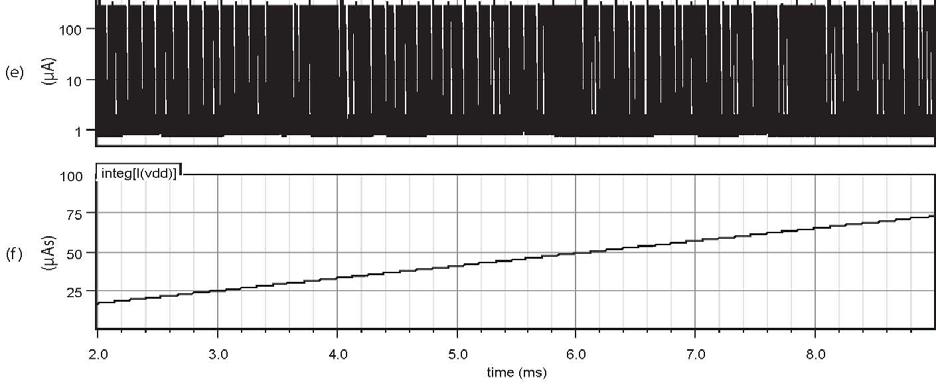
4 and surface area have been reduced for input pads in order to reduce parasitics. The total on-chip parasitic load (for purposes of die-to-die bonding) excluding transducer interconnects and bondwire has been designed to remain below 250fF and be matched to be within below 5%. Although any mismatch in parasitics will manifest itself as a static differential error, this has been maintained minimal to reduce any die-to-die variations and thus the need for postcalibration. Simulation Results: The circuit was simulated using the Cadence Spectre (5.1.41isr1) simulator with foundry supplied BSIM3v3 models. Transient simulation results for a typical capacitance variation (C N =2.5pF and C P =7.5pF) are shown in Fig. 3. This uses I bias =10nA and V ref =2V, and from Eqn. 3, the clock frequency used is determined to be: F clk =128KHz. As extracted from the simulated data, the integration phases are 1.5ms and 500µs, relating to the positive and negative differential capacitances respectively, i.e. C P and C N. This is in exact agreement with the theoretically expected from Eqn. 2. Furthermore, the counter output value, latches at: 128, again matching the expected, (i.e. OUT=F clk δτ=128k(1.5m- 0.5m). In this configuration, the average power consumption comes to 25.9µW, extracted from the results shown in Fig. 3. Conclusion: The design of a novel micropower, differential-capacitive sensor interface has been described. The front-end consisting of a current-integrating threshold detection is a commonly used technique in bio-inspired neuron circuits. Coupled with a current steering technique and up/down counter provides an easily implementable method for extracting a differential, digital reading. By using this technique, most technology-related variations and device non-idealities are eliminated. The system designed, simulated and fabricated has considered ideal capacitance elements, valid if the transducers are designed such that the combs are made stiff in the direction of the electric field, but remaining flexible out-of-plane, thus maintaining sensitivity. For micro-sensors with the electric field incident along the sense plane, the interface can be
5 altered, by implementing the current integration across a feedback capacitor in a switchedcapacitor configuration, thus biasing the sense nodes with fixed voltages and not applying a dynamic electrostatic force. The interface described herein achieves at least a 45dB dynamic range with micropower operation in a compact footprint. It is envisaged, such a front-end may be applicable within capacitive sensor arrays with each element having a dedicated interface in niche applications benefiting from embedded in-sense-plane processing. Acknowledgements: This work was supported by the Cyprus Research Promotion Foundation (RPF), grant no.: ΠΔE-0505/07. References: 1. Wu, J., et al.: A low-noise low-offset capacitive sensing amplifier for a 50-μg/pHz monolithic CMOS MEMS accelerometer, JSSC, IEEE, 2004, 39, (5), pp ; 2. Geen, J.A., et al.: Single-chip surface micromachined integrated gyroscope with 500/h Allan deviation, JSSC., IEEE, 2002, 37, (12), pp Yazdi, N., and Najafi, K.: An interface IC for a capacitive silicon μg accelerometer, ISSCC, IEEE, 1999, pp Mochizuki, K., et al.: A Relaxation-Oscillator-Based Interface for High-Accuracy Ratiometric Signal Processing of Differential-Cap. Transducers, Trans. Instr. Meas., IEEE, 1998, 47, (1), pp Krummenacher, F.: A high resolution Capacitance-to-Frequency Converter, J. Solid-State Circ., IEEE, 1985, 20, (3), pp Bracke, W., et al.: Ultra-low-power Interface Chip for Autonomous Cap. Sensor Systems, TCAS-I, IEEE, 2007, 54, (1), pp Kulah, H., Yazdi, N., and Najafi, K.: A CMOS switched-capacitor interface circuit for an integrated accelerometer, Proc. Midwest Symp. Circ. Syst., IEEE, 2000, 1, pp
6 8.. Kung, J.T., et al.,: A digital readout technique for capacitive sensor applications, JSSC., IEEE, 1988, 23, (4), pp George, B., and Kumar, V.J, Switched capacitor triple slope capacitance to digital converter, Proc. Circ. Dev. Syst., IEE, 2006, 153, (2), pp Tedja, S., et al.: A CMOS Low-Noise and Low-Power Charge Sampling Integrated Circuit for Capacitive Detector Sensor Interfaces. JSSC, IEEE, 1995, 30, (2), pp Authors affiliations: T. G. Constandinou and J. Georgiou (Holistic Electronics Research Lab, University of Cyprus, Nicosia 1678, Cyprus) t.constandinou@imperial.ac.uk C. Toumazou (Institute of Biomedical Engineering, Imperial College London, South Kensington Campus, London SW7 2AZ, United Kingdom. T. G. Constandinou is also with the Institute of Biomedical Engineering, Imperial College London.
7 Figure Captions: Fig. 1 Equivalent circuit of a differential capacitive microsensor Fig. 2 Top level circuit schematic for the sensor interface Fig. 3 Transient simulation results (for C N =2.5pF, C P =7.5pF, I bias =10nA, F clk =128KHz, V ref =2V, Vdd=3.3V). Shown are: (a) V reset, (b) V τ, (c) V CN and V CP, (d) CountQ(9:0) and Q(9:0), (e) I Vdd, and (f) integ(i Vdd ).
8 Figure 1:
9 Figure 2:
10 Figure 3:
Comparison between Analog and Digital Current To PWM Converter for Optical Readout Systems
 Comparison between Analog and Digital Current To PWM Converter for Optical Readout Systems 1 Eun-Jung Yoon, 2 Kangyeob Park, 3* Won-Seok Oh 1, 2, 3 SoC Platform Research Center, Korea Electronics Technology
ISSCC 2006 / SESSION 16 / MEMS AND SENSORS / 16.1
 16.1 A 4.5mW Closed-Loop Σ Micro-Gravity CMOS-SOI Accelerometer Babak Vakili Amini, Reza Abdolvand, Farrokh Ayazi Georgia Institute of Technology, Atlanta, GA Recently, there has been an increasing demand
Lecture 10: Accelerometers (Part I)
") Lecture 0: Accelerometers (Part I) ADXL 50 (Formerly the original ADXL 50) ENE 5400, Spring 2004 Outline Performance analysis Capacitive sensing Circuit architectures Circuit techniques for non-ideality
Lecture 0: Accelerometers (Part I) ADXL 50 (Formerly the original ADXL 50) ENE 5400, Spring 2004 Outline Performance analysis Capacitive sensing Circuit architectures Circuit techniques for non-ideality
CHAPTER 3. Instrumentation Amplifier (IA) Background. 3.1 Introduction. 3.2 Instrumentation Amplifier Architecture and Configurations
 Background. 3.1 Introduction. 3.2 Instrumentation Amplifier Architecture and Configurations") CHAPTER 3 Instrumentation Amplifier (IA) Background 3.1 Introduction The IAs are key circuits in many sensor readout systems where, there is a need to amplify small differential signals in the presence
CHAPTER 3 Instrumentation Amplifier (IA) Background 3.1 Introduction The IAs are key circuits in many sensor readout systems where, there is a need to amplify small differential signals in the presence
ISSN:
 1391 DESIGN OF 9 BIT SAR ADC USING HIGH SPEED AND HIGH RESOLUTION OPEN LOOP CMOS COMPARATOR IN 180NM TECHNOLOGY WITH R-2R DAC TOPOLOGY AKHIL A 1, SUNIL JACOB 2 1 M.Tech Student, 2 Associate Professor,
Design of Low Power CMOS Startup Charge Pump Based on Body Biasing Technique
 Design of Low Power CMOS Startup Charge Pump Based on Body Biasing Technique Juliet Abraham 1, Dr. B. Paulchamy 2 1 PG Scholar, Hindusthan institute of Technology, coimbtore-32, India 2 Professor and HOD,
A 19-bit column-parallel folding-integration/cyclic cascaded ADC with a pre-charging technique for CMOS image sensors
 LETTER IEICE Electronics Express, Vol.14, No.2, 1 12 A 19-bit column-parallel folding-integration/cyclic cascaded ADC with a pre-charging technique for CMOS image sensors Tongxi Wang a), Min-Woong Seo
SiNANO-NEREID Workshop:
 SiNANO-NEREID Workshop: Towards a new NanoElectronics Roadmap for Europe Leuven, September 11 th, 2017 WP3/Task 3.2 Connectivity RF and mmw Design Outline Connectivity, what connectivity? High data rates
A CMOS Analog Front-End Circuit for MEMS Based Temperature Sensor
 Technology Volume 1, Issue 2, October-December, 2013, pp. 01-06, IASTER 2013 www.iaster.com, Online: 2347-6109, Print: 2348-0017 A CMOS Analog Front-End Circuit for MEMS Based Temperature Sensor Bollam
Research Article Micro-Optoelectromechanical Tilt Sensor
 Hindawi Publishing Corporation Journal of Sensors Volume 2008, Article ID 782764, 7 pages doi:10.1155/2008/782764 Research Article Micro-Optoelectromechanical Tilt Sensor Timothy G. Constandinou 1, 2 and
DESIGN AND ANALYSIS OF LOW POWER CHARGE PUMP CIRCUIT FOR PHASE-LOCKED LOOP
 DESIGN AND ANALYSIS OF LOW POWER CHARGE PUMP CIRCUIT FOR PHASE-LOCKED LOOP 1 B. Praveen Kumar, 2 G.Rajarajeshwari, 3 J.Anu Infancia 1, 2, 3 PG students / ECE, SNS College of Technology, Coimbatore, (India)
Front-End and Readout Electronics for Silicon Trackers at the ILC
 2005 International Linear Collider Workshop - Stanford, U.S.A. Front-End and Readout Electronics for Silicon Trackers at the ILC M. Dhellot, J-F. Genat, H. Lebbolo, T-H. Pham, and A. Savoy Navarro LPNHE
Capacitive Sensing Project. Design of A Fully Differential Capacitive Sensing Circuit for MEMS Accelerometers. Matan Nurick Radai Rosenblat
 Capacitive Sensing Project Design of A Fully Differential Capacitive Sensing Circuit for MEMS Accelerometers Matan Nurick Radai Rosenblat Supervisor: Dr. Claudio Jacobson VLSI Laboratory, Technion, Israel,
Analog CMOS Interface Circuits for UMSI Chip of Environmental Monitoring Microsystem
 Analog CMOS Interface Circuits for UMSI Chip of Environmental Monitoring Microsystem A report Submitted to Canopus Systems Inc. Zuhail Sainudeen and Navid Yazdi Arizona State University July 2001 1. Overview
IN the design of the fine comparator for a CMOS two-step flash A/D converter, the main design issues are offset cancelation
 JOURNAL OF STELLAR EE315 CIRCUITS 1 A 60-MHz 150-µV Fully-Differential Comparator Erik P. Anderson and Jonathan S. Daniels (Invited Paper) Abstract The overall performance of two-step flash A/D converters
A Multichannel Pipeline Analog-to-Digital Converter for an Integrated 3-D Ultrasound Imaging System
 1266 IEEE JOURNAL OF SOLID-STATE CIRCUITS, VOL. 38, NO. 7, JULY 2003 A Multichannel Pipeline Analog-to-Digital Converter for an Integrated 3-D Ultrasound Imaging System Kambiz Kaviani, Student Member,
IMPLEMENTATION OF A LOW-KICKBACK-NOISE LATCHED COMPARATOR FOR HIGH-SPEED ANALOG-TO-DIGITAL DESIGNS IN 0.18
 International Journal of Electronics, Communication & Instrumentation Engineering Research and Development (IJECIERD) ISSN 2249-684X Vol. 2 Issue 4 Dec - 2012 43-56 TJPRC Pvt. Ltd., IMPLEMENTATION OF A
A Switched-Capacitor Band-Pass Biquad Filter Using a Simple Quasi-unity Gain Amplifier
 A Switched-Capacitor Band-Pass Biquad Filter Using a Simple Quasi-unity Gain Amplifier Hugo Serra, Nuno Paulino, and João Goes Centre for Technologies and Systems (CTS) UNINOVA Dept. of Electrical Engineering
A fully autonomous power management interface for frequency upconverting harvesters using load decoupling and inductor sharing
 Journal of Physics: Conference Series PAPER OPEN ACCESS A fully autonomous power management interface for frequency upconverting harvesters using load decoupling and inductor sharing To cite this article:
DUAL ULTRA MICROPOWER RAIL-TO-RAIL CMOS OPERATIONAL AMPLIFIER
 ADVANCED LINEAR DEVICES, INC. ALD276A/ALD276B ALD276 DUAL ULTRA MICROPOWER RAILTORAIL CMOS OPERATIONAL AMPLIFIER GENERAL DESCRIPTION The ALD276 is a dual monolithic CMOS micropower high slewrate operational
INTEGRATED CIRCUITS. AN109 Microprocessor-compatible DACs Dec
 INTEGRATED CIRCUITS 1988 Dec DAC products are designed to convert a digital code to an analog signal. Since a common source of digital signals is the data bus of a microprocessor, DAC circuits that are
Digitally Tuned Low Power Gyroscope
 Digitally Tuned Low Power Gyroscope Bernhard E. Boser & Chinwuba Ezekwe Berkeley Sensor & Actuator Center Dept. of Electrical Engineering and Computer Sciences University of California, Berkeley B. Boser
A Low Power Small Area Multi-bit Quantizer with A Capacitor String in Sigma-Delta Modulator
 A Low Power Small Area Multi-bit uantizer with A Capacitor String in Sigma-Delta Modulator Xuia Wang, Jian Xu, and Xiaobo Wu Abstract An ultra-low power area-efficient fully differential multi-bit quantizer
8-Bit, high-speed, µp-compatible A/D converter with track/hold function ADC0820
 8-Bit, high-speed, µp-compatible A/D converter with DESCRIPTION By using a half-flash conversion technique, the 8-bit CMOS A/D offers a 1.5µs conversion time while dissipating a maximum 75mW of power.
Single Supply, MicroPower INSTRUMENTATION AMPLIFIER
 Single Supply, MicroPower INSTRUMENTATION AMPLIFIER FEATURES LOW QUIESCENT CURRENT: µa WIDE POWER SUPPLY RANGE Single Supply:. to Dual Supply:.9/. to ± COMMON-MODE RANGE TO (). RAIL-TO-RAIL OUTPUT SWING
Multiplexer for Capacitive sensors
 DATASHEET Multiplexer for Capacitive sensors Multiplexer for Capacitive Sensors page 1/7 Features Very well suited for multiple-capacitance measurement Low-cost CMOS Low output impedance Rail-to-rail digital
EUA2011A. Low EMI, Ultra-Low Distortion, 2.5-W Mono Filterless Class-D Audio Power Amplifier DESCRIPTION FEATURES APPLICATIONS
 Low EMI, Ultra-Low Distortion, 2.5-W Mono Filterless Class-D Audio Power Amplifier DESCRIPTION The EUA2011A is a high efficiency, 2.5W mono class-d audio power amplifier. A new developed filterless PWM
Analog I/O. ECE 153B Sensor & Peripheral Interface Design Winter 2016
 Analog I/O ECE 153B Sensor & Peripheral Interface Design Introduction Anytime we need to monitor or control analog signals with a digital system, we require analogto-digital (ADC) and digital-to-analog
An Analog Phase-Locked Loop
 1 An Analog Phase-Locked Loop Greg Flewelling ABSTRACT This report discusses the design, simulation, and layout of an Analog Phase-Locked Loop (APLL). The circuit consists of five major parts: A differential
CMOS 12-Bit Serial Input Multiplying DIGITAL-TO-ANALOG CONVERTER
 CMOS 12-Bit Serial Input Multiplying DIGITAL-TO-ANALOG CONVERTER FEATURES 12-BICCURACY IN 8-PIN MINI-DIP AND 8-PIN SOIC FAST 3-WIRE SERIAL INTERFACE LOW INL AND DNL: ±1/2 LSB max GAIN ACCURACY TO ±1LSB
Analysis of 1=f Noise in CMOS Preamplifier With CDS Circuit
 IEEE TRANSACTIONS ON NUCLEAR SCIENCE, VOL. 49, NO. 4, AUGUST 2002 1819 Analysis of 1=f Noise in CMOS Preamplifier With CDS Circuit Tae-Hoon Lee, Gyuseong Cho, Hee Joon Kim, Seung Wook Lee, Wanno Lee, and
Copyright 2007 Year IEEE. Reprinted from ISCAS 2007 International Symposium on Circuits and Systems, May This material is posted here
 Copyright 2007 Year IEEE. Reprinted from ISCAS 2007 International Symposium on Circuits and Systems, 27-30 May 2007. This material is posted here with permission of the IEEE. Such permission of the IEEE
A 2.4 GHZ RECEIVER IN SILICON-ON-SAPPHIRE MICHAEL PETERS. B.S., Kansas State University, 2009 A REPORT
 A 2.4 GHZ RECEIVER IN SILICON-ON-SAPPHIRE by MICHAEL PETERS B.S., Kansas State University, 2009 A REPORT submitted in partial fulfillment of the requirements for the degree MASTER OF SCIENCE Department
Performance of a Resistance-To-Voltage Read Circuit for Sensing Magnetic Tunnel Junctions
 Performance of a Resistance-To-Voltage Read Circuit for Sensing Magnetic Tunnel Junctions Michael J. Hall Viktor Gruev Roger D. Chamberlain Michael J. Hall, Viktor Gruev, and Roger D. Chamberlain, Performance
Low Output Impedance 0.6µm-CMOS Sub-Bandgap Reference. V. Gupta and G.A. Rincón-Mora
 Low Output Impedance 0.6µm-CMOS Sub-Bandgap Reference V. Gupta and G.A. Rincón-Mora Abstract: A 0.6µm-CMOS sub-bandgap reference circuit whose output voltage is, unlike reported literature, concurrently
The Medipix3 Prototype, a Pixel Readout Chip Working in Single Photon Counting Mode with Improved Spectrometric Performance
 26 IEEE Nuclear Science Symposium Conference Record NM1-6 The Medipix3 Prototype, a Pixel Readout Chip Working in Single Photon Counting Mode with Improved Spectrometric Performance R. Ballabriga, M. Campbell,
Architectures and Design Methodologies for Very Low Power and Power Effective A/D Sigma-Delta Converters
 0 Architectures and Design Methodologies for Very Low Power and Power Effective A/D Sigma-Delta Converters F. Maloberti University of Pavia - Italy franco.maloberti@unipv.it 1 Introduction Summary Sigma-Delta
Design of High gain and Low Offset CMOS Current Mode Front End Operational Amplifier
 Design of High gain and Low Offset CMOS Current Mode Front End Operational Amplifier R.SHANTHA SELVA KUMARI 1, M.VIJAYALAKSHMI 2 1 Professor and Head, 2 Student, Department of Electronics and Communication
EUA W Mono Filterless Class-D Audio Power Amplifier DESCRIPTION FEATURES APPLICATIONS. Typical Application Circuit
 3-W Mono Filterless Class-D Audio Power Amplifier DESCRIPTION The EUA2011 is a high efficiency, 3W mono class-d audio power amplifier. A low noise, filterless PWM architecture eliminates the output filter,
Hot Topics and Cool Ideas in Scaled CMOS Analog Design
 Engineering Insights 2006 Hot Topics and Cool Ideas in Scaled CMOS Analog Design C. Patrick Yue ECE, UCSB October 27, 2006 Slide 1 Our Research Focus High-speed analog and RF circuits Device modeling,
ADC0808/ADC Bit µp Compatible A/D Converters with 8-Channel Multiplexer
 ADC0808/ADC0809 8-Bit µp Compatible A/D Converters with 8-Channel Multiplexer General Description The ADC0808, ADC0809 data acquisition component is a monolithic CMOS device with an 8-bit analog-to-digital
5μW-10mW Input Power Range Inductive Boost Converter for Indoor. Photovoltaic Energy Harvesting with Integrated Maximum Power Point
 5μW-10mW Input Power Range Inductive Boost Converter for Indoor Photovoltaic Energy Harvesting with Integrated Maximum Power Point Tracking Algorithm Yifeng Qiu 1, Chris van Liempd 1, Bert Op het Veld
ECEN689: Special Topics in High-Speed Links Circuits and Systems Spring 2012
 ECEN689: Special Topics in High-Speed Links Circuits and Systems Spring 2012 Lecture 5: Termination, TX Driver, & Multiplexer Circuits Sam Palermo Analog & Mixed-Signal Center Texas A&M University Announcements
REDUCING power consumption and enhancing energy
 548 IEEE TRANSACTIONS ON CIRCUITS AND SYSTEMS II: EXPRESS BRIEFS, VOL. 63, NO. 6, JUNE 2016 A Low-Voltage PLL With a Supply-Noise Compensated Feedforward Ring VCO Sung-Geun Kim, Jinsoo Rhim, Student Member,
DESIGN OF A NOVEL CURRENT MIRROR BASED DIFFERENTIAL AMPLIFIER DESIGN WITH LATCH NETWORK. Thota Keerthi* 1, Ch. Anil Kumar 2
 ISSN 2277-2685 IJESR/October 2014/ Vol-4/Issue-10/682-687 Thota Keerthi et al./ International Journal of Engineering & Science Research DESIGN OF A NOVEL CURRENT MIRROR BASED DIFFERENTIAL AMPLIFIER DESIGN
A 24 V Chopper Offset-Stabilized Operational Amplifier with Symmetrical RC Notch Filters having sub-10 µv offset and over-120db CMRR
 ROMANIAN JOURNAL OF INFORMATION SCIENCE AND TECHNOLOGY Volume 20, Number 4, 2017, 301 312 A 24 V Chopper Offset-Stabilized Operational Amplifier with Symmetrical RC Notch Filters having sub-10 µv offset
A flexible compact readout circuit for SPAD arrays ABSTRACT Keywords: 1. INTRODUCTION 2. THE SPAD 2.1 Operation 7780C - 55
 A flexible compact readout circuit for SPAD arrays Danial Chitnis * and Steve Collins Department of Engineering Science University of Oxford Oxford England OX13PJ ABSTRACT A compact readout circuit that
MXD2125J/K. Ultra Low Cost, ±2.0 g Dual Axis Accelerometer with Digital Outputs
 Ultra Low Cost, ±2.0 g Dual Axis Accelerometer with Digital Outputs MXD2125J/K FEATURES RoHS Compliant Dual axis accelerometer Monolithic CMOS construction On-chip mixed mode signal processing Resolution
A Prototype Amplifier-Discriminator Chip for the GLAST Silicon-Strip Tracker
 A Prototype Amplifier-Discriminator Chip for the GLAST Silicon-Strip Tracker Robert P. Johnson Pavel Poplevin Hartmut Sadrozinski Ned Spencer Santa Cruz Institute for Particle Physics The GLAST Project
A Novel High Efficient Six Stage Charge Pump
 A Novel High Efficient Six Stage Charge Pump based PLL Ms. Monica.B.J.C (Student) Department of ECE (Applied Electronics), Dhanalakshmi Srinivasan college of Engineering, Coimbatore, India. Ms. Yamuna.J
Single-Ended to Differential Converter for Multiple-Stage Single-Ended Ring Oscillators
 IEEE JOURNAL OF SOLID-STATE CIRCUITS, VOL. 38, NO. 1, JANUARY 2003 141 Single-Ended to Differential Converter for Multiple-Stage Single-Ended Ring Oscillators Yuping Toh, Member, IEEE, and John A. McNeill,
DAT175: Topics in Electronic System Design
 DAT175: Topics in Electronic System Design Analog Readout Circuitry for Hearing Aid in STM90nm 21 February 2010 Remzi Yagiz Mungan v1.10 1. Introduction In this project, the aim is to design an adjustable
Switch-less Dual-frequency Reconfigurable CMOS Oscillator using One Single Piezoelectric AlN MEMS Resonator with Co-existing S0 and S1 Lamb-wave Modes
 From the SelectedWorks of Chengjie Zuo January, 11 Switch-less Dual-frequency Reconfigurable CMOS Oscillator using One Single Piezoelectric AlN MEMS Resonator with Co-existing S and S1 Lamb-wave Modes
Research on Low Power Sigma-Delta Interface Circuit used in Capacitive Micro-accelerometers
 JOURNAL OF COMPUTERS, VOL. 7, NO. 10, OCTOBER 01 383 Research on Low Power Sigma-Delta Interface Circuit used in Capacitive Micro-accelerometers Yue Ruan, Ying Tang and Wenji Yao Zhejiang Shuren University,
LF13741 Monolithic JFET Input Operational Amplifier
 LF13741 Monolithic JFET Input Operational Amplifier General Description The LF13741 is a 741 with BI-FETTM input followers on the same die Familiar operating characteristics those of a 741 with the added
Realization of a ROIC for 72x4 PV-IR detectors
 Realization of a ROIC for 72x4 PV-IR detectors Huseyin Kayahan, Arzu Ergintav, Omer Ceylan, Ayhan Bozkurt, Yasar Gurbuz Sabancı University Faculty of Engineering and Natural Sciences, Tuzla, Istanbul 34956
ISSCC 2004 / SESSION 26 / OPTICAL AND FAST I/O / 26.6
 ISSCC 2004 / SESSION 26 / OPTICAL AND FAST I/O / 26.6 26.6 40Gb/s Amplifier and ESD Protection Circuit in 0.18µm CMOS Technology Sherif Galal, Behzad Razavi University of California, Los Angeles, CA Optical
A new class AB folded-cascode operational amplifier
 A new class AB folded-cascode operational amplifier Mohammad Yavari a) Integrated Circuits Design Laboratory, Department of Electrical Engineering, Amirkabir University of Technology, Tehran, Iran a) myavari@aut.ac.ir
OBSOLETE. High Accuracy 1 g to 5 g Single Axis imems Accelerometer with Analog Input ADXL105*
 a FEATURES Monolithic IC Chip mg Resolution khz Bandwidth Flat Amplitude Response ( %) to khz Low Bias and Sensitivity Drift Low Power ma Output Ratiometric to Supply User Scalable g Range On-Board Temperature
High Accuracy 1 g to 5 g Single Axis imems Accelerometer with Analog Input ADXL105*
 a FEATURES Monolithic IC Chip mg Resolution khz Bandwidth Flat Amplitude Response ( %) to khz Low Bias and Sensitivity Drift Low Power ma Output Ratiometric to Supply User Scalable g Range On-Board Temperature
SWS1120 Configurable 24-bit Analog-to-Digital Interface IC for High Performance Capacitive MEMS Gyroscope
 SWS1120 Configurable 24-bit Analog-to-Digital Interface IC for High Performance Capacitive MS Gyroscope General Description The SWS1120 is a full capacitive detection MS gyroscope control IC. The SWS1120
System Level Simulation of a Digital Accelerometer
 System Level Simulation of a Digital Accelerometer M. Kraft*, C. P. Lewis** *University of California, Berkeley Sensors and Actuator Center 497 Cory Hall, Berkeley, CA 94720, mkraft@kowloon.eecs.berkeley.edu
QPLL Manual. Quartz Crystal Based Phase-Locked Loop for Jitter Filtering Application in LHC. Paulo Moreira. CERN - EP/MIC, Geneva Switzerland
 QPLL Manual Quartz Crystal Based Phase-Locked Loop for Jitter Filtering Application in LHC Paulo Moreira CERN - EP/MIC, Geneva Switzerland 2004-01-26 Version 1.0 Technical inquires: Paulo.Moreira@cern.ch
Conference Guide IEEE International Symposium on Circuits and Systems. Rio de Janeiro, May 15 18, 2011
 2011 IEEE International Symposium on Circuits and Systems Rio de Janeiro, May 15 18, 2011 Conference Guide The Institute of Electrical and Eletronics Engineers IEEE Circuits and System s Society Federal
ELEN6350. Summary: High Dynamic Range Photodetector Hassan Eddrees, Matt Bajor
 ELEN6350 High Dynamic Range Photodetector Hassan Eddrees, Matt Bajor Summary: The use of image sensors presents several limitations for visible light spectrometers. Both CCD and CMOS one dimensional imagers
/$ IEEE
 IEEE TRANSACTIONS ON CIRCUITS AND SYSTEMS II: EXPRESS BRIEFS, VOL. 53, NO. 11, NOVEMBER 2006 1205 A Low-Phase Noise, Anti-Harmonic Programmable DLL Frequency Multiplier With Period Error Compensation for
A radiation tolerant, low-power cryogenic capable CCD readout system:
 A radiation tolerant, low-power cryogenic capable CCD readout system: Enabling focal-plane mounted CCD read-out for ground or space applications with a pair of ASICs. Overview What do we want to read out
A Novel General Purpose Current Mode Oscillating Circuit for the Read-Out of Capacitive Sensors
 A Novel General Purpose Current Mode Oscillating Circuit for the Read-Out of Capacitive Sensors A. De Marcellis, C. Di Carlo, G. Ferri, V. Stornelli Department of Electrical and Information Engineering,
Design of an Asynchronous 1 Bit Charge Sharing Digital to Analog Converter for a Level Crossing ADC
 Design of an Asynchronous 1 Bit Charge Sharing Digital to Analog Converter for a Level Crossing ADC Anita Antony 1, Shobha Rekh Paulson 2, D. Jackuline Moni 3 1, 2, 3 School of Electrical Sciences, Karunya
Wafer-scale 3D integration of silicon-on-insulator RF amplifiers
 Wafer-scale integration of silicon-on-insulator RF amplifiers The MIT Faculty has made this article openly available. Please share how this access benefits you. Your story matters. Citation As Published
Wafer Level Vacuum Packaged Out-of-Plane and In-Plane Differential Resonant Silicon Accelerometers for Navigational Applications
 58 ILLHWAN KIM et al : WAFER LEVEL VACUUM PACKAGED OUT-OF-PLANE AND IN-PLANE DIFFERENTIAL RESONANT SILICON ACCELEROMETERS FOR NAVIGATIONAL APPLICATIONS Wafer Level Vacuum Packaged Out-of-Plane and In-Plane
ENERGY HARVESTING FROM MOTION FOR AUTONOMOUS DEVICES
 ENERGY HARVESTING FROM MOTION FOR AUTONOMOUS DEVICES ERIC YEATMAN DEPARTMENT OF ELECTRICAL ENGINEERING IMPERIAL COLLEGE LONDON HOW DO WE GENERATE POWER? FROM MOTION HOW IS HARVESTING DIFFERENT? Local generation
AN-1106 Custom Instrumentation Amplifier Design Author: Craig Cary Date: January 16, 2017
 AN-1106 Custom Instrumentation Author: Craig Cary Date: January 16, 2017 Abstract This application note describes some of the fine points of designing an instrumentation amplifier with op-amps. We will
ECE 4430 Project 1: Design of BMR and BGR Student 1: Moez Karim Aziz Student 2: Hanbin (Victor) Ying 10/13/2016
 Ying 10/13/2016") ECE 4430 Project 1: Design of BMR and BGR Student 1: Moez Karim Aziz Student 2: Hanbin (Victor) Ying 10/13/2016 I have neither given nor received any unauthorized assistance on this project. BMR Schematic
ECE 4430 Project 1: Design of BMR and BGR Student 1: Moez Karim Aziz Student 2: Hanbin (Victor) Ying 10/13/2016 I have neither given nor received any unauthorized assistance on this project. BMR Schematic
CMOS 12-Bit Multiplying DIGITAL-TO-ANALOG CONVERTER Microprocessor Compatible
 CMOS 12-Bit Multiplying DIGITAL-TO-ANALOG CONVERTER Microprocessor Compatible FEATURES FOUR-QUADRANT MULTIPLICATION LOW GAIN TC: 2ppm/ C typ MONOTONICITY GUARANTEED OVER TEMPERATURE SINGLE 5V TO 15V SUPPLY
An accurate track-and-latch comparator
 An accurate track-and-latch comparator K. D. Sadeghipour a) University of Tabriz, Tabriz 51664, Iran a) dabbagh@tabrizu.ac.ir Abstract: In this paper, a new accurate track and latch comparator circuit
High Voltage and Temperature Auto Zero Op-Amp Cell Features Applications Process Technology Introduction Parameter Unit Rating
 Analogue Integration AISC11 High Voltage and Temperature Auto Zero Op-Amp Cell Rev.1 12-1-5 Features High Voltage Operation: 4.5-3 V Precision, Auto-Zeroed Input Vos High Temperature Operation Low Quiescent
A Low Power High Sensitivity CMOS Multivibrator Based Voltage to Frequency Convertor
 A Low Power High Sensitivity CMOS Multivibrator Based Voltage to Frequency Convertor Lesni.P. S 1, Rooha Razmid Ahamed 2 Student, Department of Electronics and Communication, RSET, Kochi, India 1 Assistant
Bridge Measurement Systems
 Section 5 Outline Introduction to Bridge Sensors Circuits for Bridge Sensors A real design: the ADS1232REF The ADS1232REF Firmware This presentation gives an overview of data acquisition for bridge sensors.
3 V/5 V Low Power, Synchronous Voltage-to-Frequency Converter AD7740*
 a FEATURES Synchronous Operation Full-Scale Frequency Set by External System Clock 8-Lead SOT-23 and 8-Lead microsoic Packages 3 V or 5 V Operation Low Power: 3 mw (Typ) Nominal Input Range: 0 to V REF
CMOS Digital Integrated Circuits Lec 11 Sequential CMOS Logic Circuits
 Lec Sequential CMOS Logic Circuits Sequential Logic In Combinational Logic circuit Out Memory Sequential The output is determined by Current inputs Previous inputs Output = f(in, Previous In) The regenerative
ThermalMax. Obsolete PRODUCT HIGHLIGHT PACKAGE ORDER INFO. 0 to 70 LX1810-CDB
 DESCRIPTION The is a Full-Bridge thermo-electric cooler (TEC) controller specifically designed for high performance opto-electronic products where precise temperature control is required. These products
Preliminary. MM7100 High-Voltage SPST Digital-Micro-Switch. Product Overview PRELIMINARY DATA SHEET, SEE PAGE 11 FOR DETAILS
 MM7100 High-Voltage SPST Digital-Micro-Switch Product Overview Features: Frequency Range: DC to 750 MHz Low On-State Resistance < 0.30Ω (typ.) Rated Voltage (AC or DC): 400V Rated Current (AC or DC): 2A
Design of Successive Approximation Analog to Digital Converter with Modified DAC
 Design of Successive Approximation Analog to Digital Converter with Modified DAC Nikhil A. Bobade Dr. Mahendra A. Gaikwad Prof. Jayshri D. Dhande Dept. of Electronics Professor Assistant Professor Nagpur
DESIGN FOR MOSIS EDUCATIONAL RESEARCH PROGRAM REPORT CMOS MAGNETIC FIELD STRUCTURES AND READ-OUT CIRCUIT. Prepared By: B.
 Grupo de Microsensores y Circuitos Integrados DESIGN FOR MOSIS EDUCATIONAL RESEARCH PROGRAM REPORT CMOS MAGNETIC FIELD STRUCTURES AND READ-OUT CIRCUIT Prepared By: B. Susana Soto Cruz Senior Research Institution:
MEMS Capacitive Sensor Interfaces: Can we Solve the Challenge?
 C2.3 MEMS Capacitive Sensor Interfaces: Can we Solve the Challenge? Robert PUERS Katholieke Universiteit Leuven, ESAT-MICAS Kasteelpark Arenberg 10; 3001 Leuven, Belgium Tel.: +32 16 32 1077 e-mail : puers@esat.kuleuven.be
An Improved Bandgap Reference (BGR) Circuit with Constant Voltage and Current Outputs
 Circuit with Constant Voltage and Current Outputs") International Journal of Research in Engineering and Innovation Vol-1, Issue-6 (2017), 60-64 International Journal of Research in Engineering and Innovation (IJREI) journal home page: http://www.ijrei.com
International Journal of Research in Engineering and Innovation Vol-1, Issue-6 (2017), 60-64 International Journal of Research in Engineering and Innovation (IJREI) journal home page: http://www.ijrei.com
A PSEUDO-CLASS-AB TELESCOPIC-CASCODE OPERATIONAL AMPLIFIER
 A PSEUDO-CLASS-AB TELESCOPIC-CASCODE OPERATIONAL AMPLIFIER M. Taherzadeh-Sani, R. Lotfi, and O. Shoaei ABSTRACT A novel class-ab architecture for single-stage operational amplifiers is presented. The structure
RESISTOR-STRING digital-to analog converters (DACs)
") IEEE TRANSACTIONS ON CIRCUITS AND SYSTEMS II: EXPRESS BRIEFS, VOL. 53, NO. 6, JUNE 2006 497 A Low-Power Inverted Ladder D/A Converter Yevgeny Perelman and Ran Ginosar Abstract Interpolating, dual resistor
IEEE TRANSACTIONS ON CIRCUITS AND SYSTEMS II: EXPRESS BRIEFS, VOL. 53, NO. 6, JUNE 2006 497 A Low-Power Inverted Ladder D/A Converter Yevgeny Perelman and Ran Ginosar Abstract Interpolating, dual resistor
ACCURATE SUPPLY CURRENT TESTING OF MIXED-SIGNAL IC USING AUTO-ZERO VOLTAGE COMPARATOR
 ACCURATE SUPPLY CURRENT TESTING OF MIXED-SIGNAL IC USING AUTO-ZERO VOLTAGE COMPARATOR Vladislav Nagy, Viera Stopjaková, Pavol Malošek, Libor Majer Department of Microelectronics, Slovak University of Technology,
Mechanical Spectrum Analyzer in Silicon using Micromachined Accelerometers with Time-Varying Electrostatic Feedback
 IMTC 2003 Instrumentation and Measurement Technology Conference Vail, CO, USA, 20-22 May 2003 Mechanical Spectrum Analyzer in Silicon using Micromachined Accelerometers with Time-Varying Electrostatic
Fractional- N PLL with 90 Phase Shift Lock and Active Switched- Capacitor Loop Filter
 J. Park, F. Maloberti: "Fractional-N PLL with 90 Phase Shift Lock and Active Switched-Capacitor Loop Filter"; Proc. of the IEEE Custom Integrated Circuits Conference, CICC 2005, San Josè, 21 September
LF442 Dual Low Power JFET Input Operational Amplifier
 LF442 Dual Low Power JFET Input Operational Amplifier General Description The LF442 dual low power operational amplifiers provide many of the same AC characteristics as the industry standard LM1458 while
A 7ns, 6mA, Single-Supply Comparator Fabricated on Linear s 6GHz Complementary Bipolar Process
 A 7ns, 6mA, Single-Supply Comparator Fabricated on Linear s 6GHz Complementary Bipolar Process Introduction The is an ultrafast (7ns), low power (6mA), single-supply comparator designed to operate on either
ADC Bit µp Compatible A/D Converter
 ADC1001 10-Bit µp Compatible A/D Converter General Description The ADC1001 is a CMOS, 10-bit successive approximation A/D converter. The 20-pin ADC1001 is pin compatible with the ADC0801 8-bit A/D family.
Multi-Element Si Sensor with Readout ASIC for EXAFS Spectroscopy 1
 Multi-Element Si Sensor with Readout ASIC for EXAFS Spectroscopy 1 Gianluigi De Geronimo a, Paul O Connor a, Rolf H. Beuttenmuller b, Zheng Li b, Antony J. Kuczewski c, D. Peter Siddons c a Microelectronics
Low-Voltage Current-Sensing CMOS Interface Circuit for Piezo-Resistive Pressure Sensor
 Low-Voltage Current-Sensing CMOS Interface Circuit for Piezo-esistive Pressure Sensor Apinunt Thanachayanont and Suttisak Sangtong A new low-voltage CMOS interface circuit with digital output for piezo-resistive
ECEN 720 High-Speed Links: Circuits and Systems. Lab3 Transmitter Circuits. Objective. Introduction. Transmitter Automatic Termination Adjustment
 1 ECEN 720 High-Speed Links: Circuits and Systems Lab3 Transmitter Circuits Objective To learn fundamentals of transmitter and receiver circuits. Introduction Transmitters are used to pass data stream
Operational Amplifier with Two-Stage Gain-Boost
 Proceedings of the 6th WSEAS International Conference on Simulation, Modelling and Optimization, Lisbon, Portugal, September 22-24, 2006 482 Operational Amplifier with Two-Stage Gain-Boost FRANZ SCHLÖGL
Highly Efficient Resonant Wireless Power Transfer with Active MEMS Impedance Matching
 Highly Efficient Resonant Wireless Power Transfer with Active MEMS Impedance Matching Bernard Ryan Solace Power Mount Pearl, NL, Canada bernard.ryan@solace.ca Marten Seth Menlo Microsystems Irvine, CA,