MAHARASHTRA STATE BOARD OF TECHNICAL EDUCATION (Autonomous) (ISO/IEC Certified)
|
|
|
- Merry Ross
- 5 years ago
- Views:
Transcription
1 WINTER 18 EXAMINATION Subject Name: Basic Electronics Model Answer Subject Code: I m p o r t a n t I n s t r u c t i o n s t o e x a m i n e r s : 1) The answers should be examined by key words and not as word-to-word as given in the model answer scheme. 2) The model answer and the answer written by candidate may vary but the examiner may try to assess the understanding level of the candidate. 3) The language errors such as grammatical, spelling errors should not be given more Importance (Not applicable for subject English and Communication Skills. 4) While assessing figures, examiner may give credit for principal components indicated in the figure. The figures drawn by candidate and model answer may vary. The examiner may give credit for any equivalent figure drawn. 5) Credits may be given step wise for numerical problems. In some cases, the assumed constant values may vary and there may be some difference in the candidate s answers and model answer. 6) In case of some questions credit may be given by judgement on part of examiner of relevant answer based on candidate s understanding. 7) For programming language papers, credit may be given to any other program based on equivalent concept. Page 1 of 28
2 Q. No. Su b Q. N. Answer Marking Scheme 1 Attempt any TEN of the following: 20 a) Draw the symbols of Schottkey-diode and Varactor diode. Schottkey-diode 1 mark each Varactor diode b) Define ripple factor and PIV of HWR (1M Each) Ripple Factor: Ripple Factor is defined as the ratio of RMS value of the AC component of output to the DC or average value of the output. PIV: Peak Inverse Voltage (PIV) is defined as the maximum negative voltage which appears across non-conducting reverse biased diode. c) State the types of filters. ( 4 Types-2M) Page 2 of 28
3 Types of filters: 1. Capacitor input filter (shunt capacitor filter) 2. Choke input filter (series inductor filter) 3. LC filter 4. π type filter OR CLC filter 5. RC filter. d) List various transistor biasing methods. Types of biasing methods: (Any 4 Biasing Methods-2M) i. Base bias (or fixed bias) ii. Base bias with emitter feedback. iii. Base bias with collector feedback iv. Voltage divider bias (or self bias) v. Emitter bias. e) Define α and β of the transistor. (1M Each) α: The ratio of collector current IC to emitter current IE for a constant collector to in the CB configuration is called current gain alpha (α). base voltage VCB β : The ratio of collector current IC to base current IB for a constant collector to emitter voltage VCE in the CE configuration is called current gain beta (β). f) State reason BJT is called as bipolar junction transistor. BJT is called bipolar junction transistor because in BJT current conduction takes place due to majority as well as minority charge carriers. (Correct reason- 2M) g) State the application of FET (any four). Applications of FET: (Any Four) (Four application-2m) i. It is used as a high impedance wideband amplifier. ii. It is used as a buffer amplifier. iii. It is used as an electronic switch. iv. It is used as a phase-shift oscillator. Page 3 of 28
4 v. It is used as a constant current source. vi. It is used as a voltage variable resistor (VVR) or voltage dependent resistor (VDR) h) Define line regulation and load regulation. (1M Each) Line regulation: The line regulation rating of a voltage regulator indicates the change in output voltage that will occur per unit change in the input voltage. Load Regulation: The load regulation indicates the change in output voltage that will occur per unit change in load current. i) State the Barkhausen criteria of oscillations. Barkhausen s criteria: (Correct Statement-2M) 1. Loop gain (β.av) should be Phase shift between the input and output signal must be equal to or 0 0. j) Sketch symbol of NAND gate and NOR gate. (1M Each) k) Convert: i) (AFB2) 16 =(?) 10 ii) (43) 8 = (?) 2 ( 1M Each) i)(afb2) 16 =(?) 10 = (10*16³+15*16²+11*16¹+2*16⁰) 1 = (44978) 10 ii) (43) 8 = (?) = ( ) 2 Page 4 of 28
 n) State the need of biasing of BJT.")
5 l) Give the different types of amplifier coupling. ( 4 Types-2M) 1. Resistance capacitance (RC) coupling. 2. Inductance (LC) coupling. 3. Transformer coupling (TC) 4. Direct coupling (D.C.) m) Sketch output characteristics of CE configuration. Show all the regions. (Correct Sketch-2M) n) State the need of biasing of BJT. Need of biasing: (Correct need- 2M) The basic need of transistor biasing is to keep the base-emitter (B-E) junction properly forward biased and the collector-emitter (C-E) junction properly reverse biased during the application of A.C. signal. This type of transistor biasing is necessary for normal and proper operation of transistor to be used for amplification. 2 Attempt any FOUR of the following: 16 a) Describe working principle of LED with diagram. Diagram: (Diagram-2M, Working principle-2m) Page 5 of 28
6 Working: A PN junction diode, which emits light when forward biased, is known as a Light Emitting Diode (LED). The emitted light may be visible or invisible. The amount of light output is directly proportional to the forward current. Thus, higher the forward current, higher is the light output. When the LED is forward biased, the electrons and holes move towards the junction and the recombination takes place. After recombination, the electrons, lying in the conduction bands of N region, fall into the holes lying in the valence band of a P region. The difference of energy between the conduction band and valence band of a P region is radiated in the form of light energy. The semiconducting materials used for manufacturing of Light Emitting Diodes are Gallium Phosphide and gallium Arsenide Phosphide. These materials decide the colour of the light emitted by the diode. b) Describe thermal runaway of transistor and explain how it can be avoided. Thermal Runaway (Description- 2M, How it avoided-2m) The reverse saturation current in semiconductor devices changes with temperature. The reverse saturation current approximately doubles for every 100 c rise in temperature. As the leakage current of transistor increases, collector current (Ic) increases The increase in power dissipation at collector base junction. This in turn increases the collector base junction causing the collector current to further increase. This process becomes cumulative. & it is possible that the ratings of the transistor are exceeded. If it happens, the device gets burnt out. This process is known as Thermal Page 6 of 28
7 Runaway. Thermal runaway can be avoided by 1) Using stabilization circuitry 2) Heat sink c) Compare half wave rectifier and full wave rectifier on the basis of: i) No. of diode ii) PIV iii) Ripple factor iv) Type of transformer used (1M Each) Rectifier Parameters Half-wave Rectifier Full wave Centre tap Rectifier Full wave Bridge Rectifier No. of diode PIV Vm 2 Vm Vm Ripple factor Type of transformer used step up or step down transformers Centre tap step up or step down transformers step up or step down transformers d) Describe the functional pin diagram of regulator IC 78XX and 79XX. ( 2M Each -1 mks diagram,. 1mks explanation) IC 78XX: Explanation: 78XX series of IC regulators is representative of three terminal devices that are available with several fixed positive output voltages. It has three terminals labeled as input, output and ground. The last two digits (mark XX) in the part no. designate the input voltage. Above fig. shows a standard configuration of a fixed positive voltage IC regulator of 78XX series. The capacitor C1 is required only if the power supply filter is located more than three inches from the IC regulator. The capacitor C0 acts basically as a line filter to improve transient response. Page 7 of 28
8 IC 79XX: Explanation: 79xx series of voltage regulators are the commonly used negative voltage regulators. These are three terminal regulators and is available with fixed output voltages of -5V, -12V and -15V. These ICs have internal current limiting protection and thermal shut down protection to protect the ICs from overload conditions. IC 79xx is used in circuits as shown in the circuit. In order to improve stability two capacitors C1 and C2 are used. The capacitor C1 is used only if the regulator is separated from filter capacitor by more than 3". It must be a 2.2 μf solid tantalum capacitor or 25μF aluminum electrolytic capacitor. The capacitor C2 is required for stability. Usually 1 μf solid tantalum capacitor is used. One can also use 25μF aluminum electrolytic capacitor. Values given may be increased without limit. Usually 1 μf solid tantalum capacitor is used. One can also use 25μF aluminum electrolytic capacitor. Values given may be increased without limit. e) Explain with circuit diagram fixed bias method of BJT. (Diagram-2M, Explanation- 2M) Explanation: The biasing circuit shown by Figure has a base resistor R B connected between the base and the V CC. Here the base-emitter junction of the transistor is forward biased by the voltage drop across R B which is the result of I B flowing through it. From the figure, the mathematical expression for I B is obtained as Here the values of V CC and V BE are fixed while the value for RB is constant once the circuit is designed. This leads to a constant value for I B resulting in a fixed operating point due to which the circuit is named as fixed base bias. This kind of bias, results in a stability factor of (β+1) which leads to very poor thermal stability. The reason behind this is the fact the β-parameter of a transistor is unpredictable and varies up to a large extent even in the case of transistor with the same model and type. This variation in β results in large changes in I C which cannot be compensated by any means in the proposed design. Hence it can be concluded that this kind Page 8 of 28
9 of β dependent bias is prone to the changes in operating point brought about by the variations in transistor characteristics and temperature. However it is to be noted that fixed base bias is most simple and uses less number of components. Moreover it offers the chance for the user to change the operating point anywhere in the active region just by changing the value of R B in the design. Further it offers no load on the source as there is no resistor across base-emitter junction. Due to these factors this kind of biasing is used in switching applications and to achieve automatic gain control in the transistors. Here, the expressions for other voltages and currents are given as f) State advantages and disadvantages of positive and negative feedback related to oscillator. (2M Each) 3 a) Attempt any FOUR of the following: Describe operating principle of photo diode with neat diagram. 16 (Diagram-2M, Operating Principle-2M) Page 9 of 28

10 Operating Principle: The photodiode is a p-n junction semiconductor diode which is always operated in the reverse biased condition. The light is always focused through a glass lens on the junction of the photodiode. As the photodiode is reverse biased, the depletion region is quite wide, penetrated on both sides of the junction, as shown in fig a. The photons incident on the depletion region will impart their energy to the ions present there and generate electron hole pairs The number of electron hole pairs will be dependent on the intensity of light (number of photons). These electrons and holes will be attracted towards the positive and negative terminals respectively of the external source, to constitute the photo current. With increase in the light intensity, more number of electron hole pairs are generated and the photocurrent increases. Thus the photocurrent is proportional to the light intensity. b) Explain with circuit diagram two stage transformer coupled amplifier using transistors. - (diagram = 2 marks, Explanation = 2 marks) Page 10 of 28

11 fig: two stage transformer coupled amplifier using transistors Explanation: The function of a coupling transformer T1 is to couple the output AC signal from the output of the first stage to the input of the second stage,while transformer T2 couples the output of AC signal to the load RL. The input capacitor C1 is used to couple the input signal to the base of transistor Q1. The capacitor CE connected at the emitters of transistor Q1 and Q2 are used to bypass the emitter to ground. The resistors R1, R2, RE and a capacitor CE form the DC biasing and stabilization. Note that, in this circuit, there is no coupling capacitor. The DC isolation between the two stages is provided by the transformer itself. There exists no DC path between primary and secondary windings of a transformer. c) Draw the circuit of centre tapped rectifier with LC filter, also draw input output waveforms. (Circuit diagram-2m, Waveforms- 2M) Page 11 of 28

12 d) Draw V. I. characteristics of UJT and explain its working principle. [Characteristics -2M, working principle- 2 M] Fig: V. I. characteristics of UJT Explanation- The VI characteristic of UJT is curve showing the relation between emitter voltage VE and emitter current IE of a UJT at a given inter base voltage VBB. Page 12 of 28

 Describe the working principle of N channel enhancement MOSFET.")
13 1. From above graph it is noted that when emitter voltage less than peak point voltage a very small current flows through UJT, IEo and in this region UJT is in the cut-off region. 2. Once conduction is established at VE = VP the emitter potential VE starts decreasing with the increase in emitter current IE. This Corresponds exactly with the decrease in resistance RB for increasing current IE. Emitter voltage decreases upto valley point. 3. After valley point any further increase in emitter current IE places the device in the saturation region. e) Describe the working principle of N channel enhancement MOSFET. (Diagram:2 M & Explanation :2M ) f) Explain crystal oscillator with circuit diagram. (Circuit diagram 2M, explanation- 2 M) Page 13 of 28
14 Explanation- To excite a crystal for operation in the series-resonant mode it may be connected as a series element in a feedback path, the crystal impedance is the smallest and the amount of positive feedback is the largest. Resistor R1, R2 and RE provide a voltage-divider stabilized dc bias circuit, the capacitor CE provides ac bypass of the emitter resistor RE and the radio-frequency coil (RFC) provides for dc bias -while decoupling any ac signal on the power lines from affecting the output signal. The voltage feedback signal from the collector to the base is maximum when the crystal impedance is minimum. The coupling capacitor Cc has negligible impedance at the circuit operating frequency but blocks any dc between collector and base. The circuit shown in figure is generally called the Pierce crystal. The resulting circuit frequency of oscillations is set by the series resonant frequency of the crystal. Variations in supply voltage, transistor parameters, etc. have no effect on the circuit operating frequency which is held stabilized by the crystal. The circuit frequency stability is set by the crystal frequency stability, which is good. The resonant frequency is given as- Fo = 1/( 2 π LC ) 4 Attempt any FOUR of the following: 16 a) Draw VI characteristics of P-N junction diode in forward and reverse bias. Define static and dynamic resistance. [Forward characteristics 1M, Reverse characteristics 1M, Definition: static resistance-1m, Dynamic resistance - 1M] Page 14 of 28
15 b) Explain with circuit diagram transistorized shunt voltage regulator. Diagram-2M, Explanation- 2M Page 15 of 28

16 Fig: transistorized shunt voltage regulator. Explanation/ Operation: 1. From Fig. the output voltage is given by. Vo = Vz+V BE 2.V in is the unregulated de power supply sending a current I, through the limiting resistor R. 3.Regulation action: If the output voltage decreases due to any reason. then ( V z + V BE ) will also decrease. But V z is constant so V BE will decrease. This will reduce the collector current I c. So more current will flow through the load and the load voltage will increase. If the output voltage increases. then exactly opposite action will take place to regulate the output voltage. c) Compare CB and CE configurations w.r.t. (i) input resistance (ii) Output resistance (1M for each parameter) (iii) current gain (iv) voltage gain Page 16 of 28
 Fig: Emitter bias circuit In the emitter bias circuit, both positive as well as negative supply voltages (+ V cc and - V EE ) are used as shown in Fig.")
.")
17 d) Describe the emitter biasing technique of BJT with ckt. Diagram. (circuit diagram-2m, Description- 2M) Fig: Emitter bias circuit In the emitter bias circuit, both positive as well as negative supply voltages (+ V cc and - V EE ) are used as shown in Fig. In this circuit the negative supply voltage - V EE is used to forward bias the base-emitter junction. TIle positive supply voltage + Vcc is used to reverse bias the collector-base junction. Analysis of Emitter bias: Step 1 : Obtain the expression for IB : Refer to the base loop shown in Fig~ (b). Apply KVL to the base loop to write, V EE IB RB + V BE + IERE Step 2 : Obtain the expression for Ie : But IE (1 + ~)lb.. V EE IB RB + V BE + (1 + ~) IB RE V EE :- V BE IB.. RB + (1 +~) RE... (7.7.1) Page 17 of 28
 ~ RB")

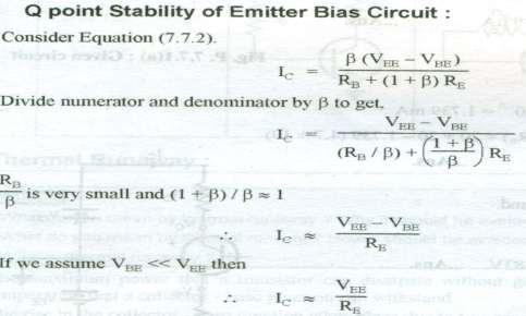
18 (V EE - V BE ) ~ RB + (1 +~) RE Page 18 of 28
19 e) Draw and explain the circuit diagram of class A push pull amplifier. [ Circuit diagram: 2M, Explanation: 2M] Fig: class A push pull amplifier. Explanation: The transformer T1 is used to as a phase splitter.the input signal the phase splited signals being applied to the base of each transistors. When Q1 is driven positive using the first half of its input signal, the collector current of Q1 increases. At the same time Q2 is driven negative using the first half of its input signal and so the collector current of Q2 decreases. From the figure you can understand that the collector currents of Q1 and Q2 ie; I1 and I2 flows in the same direction trough the corresponding halves of the T2 primary. As a result an amplified version of the original input signal is induced in the T2 secondary. It is clear that the current through the T2 secondary is the difference between the two collector currents. f) Define terms: (i) Drain resistance (iii) Amplification factor (ii) Mutual conductance (iv) pinch off voltage of FET 1M for each definition (i) Drain Resistance: DC drain resistance, also known as static or ohmic resistance of channel, is expressed as, OR Page 19 of 28
. It is the ratio of small change in drain current to corresponding change in gate to source voltage.")
20 AC drain resistance, also known as dynamic resistance of channel, is defined as resistance between drain to source when JFET is operating in pinch-off or saturation region and expressed as, (ii) Mutual conductance : It is also known as forward transconductance (gm). It is the ratio of small change in drain current to corresponding change in gate to source voltage. (iii) Amplification Factor: It is defined as the ratio of small change in drain voltage to small change in gate voltage at constant drain current. (iv) Pinch-off Voltage: It is the value of the drain to source voltage VDS at which the drain current ID reaches its constant saturation value. Any further increase in VDS does not have any effect on the value of ID. It is denoted by VP. 5 Attempt any FOUR of the following : 16 a) Draw the circuit diagram of direct coupled amplifier and explain function of each component. ( Circuit diagram -2M, Function of components- 2M) OR Page 20 of 28
 State applications of FET and MOSFET. Applications of FET: 1.")
21 Function of components: 1. Transistors Q1 and Q2 used to provide gain 2. R1 and R2 form a voltage or potential divider network used for biasing purpose 3. RE1 and RE2 are used for stabilization of operating point against temperature and β variations. b) State applications of FET and MOSFET. Applications of FET: 1. FETs are widely used as input amplifiers in oscilloscopes 2. input amplifiers electronic voltmeters and other measuring and testing equipment (Any relevant two applications of Each 2M) 3. Chopper switch 4. Current limiter circuit Applications of MOSFET: 1.MOSFET as an analog switch 2.Depletion MOSFET as a linear regulator 3.Depletion MOSFET as a linear LED driver 4.In current limiter c) Describe the working of transistor as a switch with neat circuit diagram. Transistor as Switch: A transistor can be used for two types of applications viz. amplification and switching. For amplification, the transistor is biased in its active region. For switching applications, transistor is biased to operate in the saturation (full on) ( Circuit diagram - 2M,Working - 2M for each on condition and off condition) or cut-off (full off) region. Page 21 of 28
22 (i) Transistor in cut-off region (Open switch): Fig(a) In the cut-off region, both the junctions of transistor are reverse biased and very small reverse current flows through the transistor. The voltage drop across the transistor (VCE) is high, nearly equal to supply voltage VCC. Thus, in cut-off region the transistor is equivalent to an open switch as shown in fig.(a). (ii) Transistor in Saturation region (Closed switch): Fig.(b) When Vin is positive, a large base current flows and transistor saturates. In the saturation region, both the junctions of transistor are forward biased. The collector current is very large, the voltage drop across the transistor (VCE) is very small, of the order of 0.2V to 1 V, depending on the type of transistor. Thus in saturation region, the transistor is equivalent to a closed switch. d) Describe the working of Hartley Oscillator with neat diagram. Circuit diagram: (Circuit diagram- 2M, Working- 2M) Page 22 of 28

23 Working: When the DC supply (Vcc) is given to the circuit, the collector current starts raising and begins with the charging of the capacitor C. Once capacitor C is fully charged, it starts discharging through L1 and L2 and again starts charging. This back-and-fourth voltage waveform is a sine wave which is a small and leads with its negative alteration. It will eventually die out unless it is amplified. The sine wave generated by the tank circuit is coupled to the base of the transistor through the capacitor CC1. Thus the transistor provides amplification along with inversion to amplify.the mutual inductance between L1 and L2 provides the feedback of energy from collector-emitter circuit to the base-emitter circuit. In this circuit tank circuit provides 180ºphase shift and CE transistor provides 180ºphase shift and total phase shift around the loop is 360º. e) Explain how zener diode is used as a voltage regulator. Circuit diagram of Zener Diode as Voltage Regulator: ( Circuit diagram-2m, Explanation- 2M) Page 23 of 28
24 Working For proper operation, the input voltage Vi must be greater than the Zener voltage Vz. This ensures that the Zener diode operates in the reverse breakdown condition. The unregulated input voltage Vi is applied to the Zener diode. Suppose this input voltage exceeds the Zener voltage. This voltage operates the Zener diode in reverse breakdown region and maintains a constant voltage, i.e. Vz = Vo across the load inspite of input AC voltage fluctuations or load current variations. The input current is given by, IS = Vi Vz / Rs = Vi Vo / Rs We know that the input current IS is the sum of Zener current Iz and load current IL. Therefore, IS = Iz + IL or Iz = Is - IL As the load current increase, the Zener current decreases so that the input current remains constant. According to Kirchhoff s voltage law, the output voltage is given by, Vo = Vi Is. Rs As the input current is constant, the output voltage remains constant (i.e. unaltered or unchanged). The reverse would be true, if the load current decreases. This circuit is also correct for the changes in input voltage. As the input voltage increases, more Zener current will flow through the Zener diode. This increases the input voltage Is, and also the voltage drop across the resistor Rs, but the load voltage Vo would remain constant. The reverse would be true, if the decrease in input voltage is not below Zener voltage Thus, a Zener diode acts as a voltage regulator and the fixed voltage is maintained across the load resistor RL. f) State applications of digital electronics Many of our household items make use of digital electronics. This could include laptops, televisions, remote controls and other entertainment systems, (Any four applications for -4M) 1. Kitchen appliances like microwave oven, dishwashers and washing machines. 2. Computers are one of the most complex examples and will make use of numerous, complex circuits. 3. Elevator displays 4. Traffic lights 5. In Digital Watch 6. In Networking Communication Page 24 of 28
 Construction: It formed by a contact of an N-type semiconductor substrate and tungsten or phosphor bronze wire (Cat whisker).")
25 6 Attempt any FOUR of the following: 16 a) Draw and explain construction of point contact diode. Ans :- (Construction- 2M,Explanatio n-2m) Construction: It formed by a contact of an N-type semiconductor substrate and tungsten or phosphor bronze wire (Cat whisker). The semiconductor used in the construction of point contact diode can be either silicon or germanium but Germanium is used extensively because it possesses higher carrier mobility. The dimension of the semiconductor substrate is about 1.25 mm square and its thickness is 0.5 mm thick. One phase of the semiconductor substrate is soldered to the metal base by the technique of radio frequency heating. b) Define term w.r.t. transistor. (i) DC load line (Each definition -2M) (ii) Operating point DC load line: The dc load line is the locus of I C and V CE at which BJT remains in active region i.e. it represents all the possible combinations of I C and V CE for a given amplifier. Operating point: Operating point is also called Q-point. The dc operating point between saturation and cutoff is called the Q-point. The goal is to set the Q-point such that that it does not go into saturation or cutoff when an a ac signal is applied. It is operating point of the transistor (ICQ,VCEQ) at which it is biased. Page 25 of 28
 1) Tranformer : It is used to convert ac voltage either ac high value or ac low value as per requirement")
26 c) Draw the block diagram of DC regulated power supply and state function of each block. Ans : Block diagram of regulated power supply: (Block diagram 2 M, Function of each block 2 M) 1) Tranformer : It is used to convert ac voltage either ac high value or ac low value as per requirement 2) Rectifier : Rectifier converts the transformer secondary a.c. voltage into pulsating voltage. 3) Filter : The pulsating d.c. voltage is applied to the filter it reduces the pulsations in the rectifier d.c. output voltage. Basically filter is used to remove ac components which are present in the rectifier output. 4) Voltage regulator : Finally, the voltage regulator performs two functions. Firstly, it reduces the variations in the filtered output voltage. Secondly, it keeps the output voltage (Vout) nearly constant whether the load current changes or there is change in input a.c. voltage. d) Compare BJT and FET (any 4 points). (Any four points for 4M) Sr. no. BJT JFET 1. It is bipolar device i.e. current in the device is carried by electrons and holes. 2. It is current controlled device i.e. base current controls the collector current. 3. Input resistance is low, of the order of several KΩ 4. It has positive temperature coefficient of resistance at high current levels i.e. current increases as the temperature increases. It is unipolar device i.e. current in the device is carried by either electrons or holes. It is voltage controlled device i.e. voltage at the gate terminal controls the amount of current flowing through the device. Input resistance is very high, of the order of several MΩ It has negative temperature coefficient of resistance at high current levels i.e. current decreases as the temperature increases. Page 26 of 28
27 e) Describe EX-OR gate Draw its symbol and truth table. ( Symbol - 1M,Truth Table-1M, Description- 2M) Output of an Exclusive-OR gate ONLY goes HIGH when its two input terminals are at DIFFERENT logic levels with respect to each other and output of an Exclusive-OR gate ONLY goes LOW when its two input terminals are at SIMMILAR logic levels. Boolean expression of EX-OR gate is: f) Draw circuit diagram of colpitts oscillator.colpitts oscillator has C 1 = 250 PF, C 2 =100PF and L=60 µh. Find the value of frequency of oscillation. Circuit Diagram: Given : C1=250PF, C2=100PF, L=60µH Find f osc Page 27 of 28
28 C1=250PF=250*10-12 F, C2=100PF=100*10-12 F L=60µH= 60*10-6 H Frequency of oscillation =2.431MH z Page 28 of 28
MAHARASHTRA STATE BOARD OF TECHNICAL EDUCATION (Autonomous) (ISO/IEC Certified) Summer 2016 EXAMINATIONS.
 (ISO/IEC Certified) Summer 2016 EXAMINATIONS.") Summer 2016 EXAMINATIONS Subject Code: 17321 Model Answer Important Instructions to examiners: 1) The answers should be examined by key words and not as word-to-word as given in the answer scheme. 2) The
Summer 2016 EXAMINATIONS Subject Code: 17321 Model Answer Important Instructions to examiners: 1) The answers should be examined by key words and not as word-to-word as given in the answer scheme. 2) The
WINTER 14 EXAMINATION. Model Answer. 1) The answers should be examined by key words and not as word-to-word as given in the
 The answers should be examined by key words and not as word-to-word as given in the") WINTER 14 EXAMINATION Subject Code: 17213 Model Answer Important Instructions to examiners: 1) The answers should be examined by key words and not as word-to-word as given in the model answer scheme. 2)
WINTER 14 EXAMINATION Subject Code: 17213 Model Answer Important Instructions to examiners: 1) The answers should be examined by key words and not as word-to-word as given in the model answer scheme. 2)
Subject Code: Model Answer Page No: / N
 Important Instructions to examiners: 1) The answers should be examined by key words and not as word-to-word as given in the model answer scheme. 2) The model answer and the answer written by candidate
MAHARASHTRA STATE BOARD OF TECHNICAL EDUCATION (Autonomous) (ISO/IEC Certified) MODEL ANSWER
 (ISO/IEC Certified) MODEL ANSWER") Important Instructions to examiners: 1) The answers should be examined by key words and not as word-to-word as given in the model answer scheme. 2) The model answer and the answer written by candidate
Important Instructions to examiners: 1) The answers should be examined by key words and not as word-to-word as given in the model answer scheme. 2) The model answer and the answer written by candidate
Q1 A) Attempt any six: i) Draw the neat symbol of N-channel and P-channel FET
 Attempt any six: i) Draw the neat symbol of N-channel and P-channel FET") Subject Code:17319 Model Answer Page1 of 27 Important Instructions to examiners: 1) The answers should be examined by key words and not as word-to-word as given in the model answer scheme. 2) The model
Subject Code:17319 Model Answer Page1 of 27 Important Instructions to examiners: 1) The answers should be examined by key words and not as word-to-word as given in the model answer scheme. 2) The model
MAHARASHTRA STATE BOARD OF TECHNICAL EDUCATION (Autonomous) (ISO/IEC Certified)
 (ISO/IEC Certified)") WINTER 16 EXAMINATION Model Answer Subject Code: 17213 Important Instructions to examiners: 1) The answers should be examined by key words and not as word-to-word as given in the model answer scheme. 2)
WINTER 16 EXAMINATION Model Answer Subject Code: 17213 Important Instructions to examiners: 1) The answers should be examined by key words and not as word-to-word as given in the model answer scheme. 2)
MAHARASHTRA STATE BOARD OF TECHNICAL EDUCATION (Autonomous) (ISO/IEC Certified)
 (ISO/IEC Certified)") WINTER 2017 EXAMINATION Subject Name: Basic Electronics Model Answer Subject Code: 17321 Important Instructions to examiners: 1) The answers should be examined by key words and not as word-to-word as given
WINTER 2017 EXAMINATION Subject Name: Basic Electronics Model Answer Subject Code: 17321 Important Instructions to examiners: 1) The answers should be examined by key words and not as word-to-word as given
SUMMER 13 EXAMINATION Subject Code: Model Answer Page No: / N
 Important Instructions to examiners: 1) The answers should be examined by key words and not as word-to-word as given in the model answer scheme. 2) The model answer and the answer written by candidate
MODEL ANSWER SUMMER 17 EXAMINATION 17319
 MODEL ANSWER SUMMER 17 EXAMINATION 17319 Subject Title: Electronics Devices and Circuits. Subject Code: Important Instructions to examiners: 1) The answers should be examined by key words and not as word-to-word
Scheme Q.1 Attempt any SIX of following 12-Total Marks 1 A) Draw symbol of P-N diode, Zener diode. 2 M Ans: P-N diode
 Draw symbol of P-N diode, Zener diode. 2 M Ans: P-N diode") Q. No. WINTER 16 EXAMINATION (Subject Code: 17321) Model Answer Important Instructions to examiners: 1) The answers should be examined by key words and not as word-to-word as given in themodel answer scheme.
Q. No. WINTER 16 EXAMINATION (Subject Code: 17321) Model Answer Important Instructions to examiners: 1) The answers should be examined by key words and not as word-to-word as given in themodel answer scheme.
MAHARASHTRA STATE BOARD OF TECHNICAL EDUCATION (Autonomous) (ISO/IEC Certified) Subject Code: Model Answer Page No: 1/
 (ISO/IEC Certified) Subject Code: Model Answer Page No: 1/") MAHARASHTRA STATE BOARD OF TECHNICAL EDUCATION (Autonomous) (ISO/IEC 27001 2005 Certified) SUMMER 13 EXAMINATION Subject Code: 12025 Model Answer Page No: 1/ Important Instructions to examiners: 1) The
MAHARASHTRA STATE BOARD OF TECHNICAL EDUCATION (Autonomous) (ISO/IEC 27001 2005 Certified) SUMMER 13 EXAMINATION Subject Code: 12025 Model Answer Page No: 1/ Important Instructions to examiners: 1) The
Scheme Q.1 Attempt any SIX of following: 12-Total Marks a) Draw symbol NPN and PNP transistor. 2 M Ans: Symbol Of NPN and PNP BJT (1M each)
 Draw symbol NPN and PNP transistor. 2 M Ans: Symbol Of NPN and PNP BJT (1M each)") Q. No. WINTER 16 EXAMINATION (Subject Code: 17319) Model Answer Important Instructions to examiners: 1) The answers should be examined by key words and not as word-to-word as given in the model answer
Q. No. WINTER 16 EXAMINATION (Subject Code: 17319) Model Answer Important Instructions to examiners: 1) The answers should be examined by key words and not as word-to-word as given in the model answer
F.Y. Diploma : Sem. II [CO/CD/CM/CW/IF] Basic Electronics
![F.Y. Diploma : Sem. II [CO/CD/CM/CW/IF] Basic Electronics](/thumbs/78/77332946.jpg "F.Y. Diploma : Sem. II [CO/CD/CM/CW/IF] Basic Electronics") F.Y. Diploma : Sem. II [CO/CD/CM/CW/IF] Basic Electronics Time : 3 Hrs.] Prelim Question Paper Solutions [Marks : 100 Q.1 Attempt any TEN of the following : [20] Q.1(a) Give the classification of capacitor.
F.Y. Diploma : Sem. II [CO/CD/CM/CW/IF] Basic Electronics Time : 3 Hrs.] Prelim Question Paper Solutions [Marks : 100 Q.1 Attempt any TEN of the following : [20] Q.1(a) Give the classification of capacitor.
Summer 2015 Examination. 1) The answers should be examined by key words and not as word-to-word as given in the model answer scheme.
 The answers should be examined by key words and not as word-to-word as given in the model answer scheme.") Summer 2015 Examination Subject Code: 17213 Model Answer Important Instructions to examiners: 1) The answers should be examined by key words and not as word-to-word as given in the model answer scheme.
Summer 2015 Examination Subject Code: 17213 Model Answer Important Instructions to examiners: 1) The answers should be examined by key words and not as word-to-word as given in the model answer scheme.
OBJECTIVE TYPE QUESTIONS
 OBJECTIVE TYPE QUESTIONS Q.1 The breakdown mechanism in a lightly doped p-n junction under reverse biased condition is called (A) avalanche breakdown. (B) zener breakdown. (C) breakdown by tunnelling.
MODEL ANSWER SUMMER 17 EXAMINATION 17213
 MODEL ANSWER SUMMER 17 EXAMINATION 17213 Subject Title: Basic Electronics Subject Code: Important Instructions to examiners: 1) The answers should be examined by key words and not as word-to-word as given
MAHARASHTRA STATE BOARD OF TECHNICAL EDUCATION (Autonomous) (ISO/IEC Certified) Summer 2016 EXAMINATIONS
 (ISO/IEC Certified) Summer 2016 EXAMINATIONS") Summer 2016 EXAMINATIONS Subject Code: 17213 Model Answer Important Instructions to examiners: 1) The answers should be examined by key words and not as word-to-word as given in the answer scheme. 2) The
Summer 2016 EXAMINATIONS Subject Code: 17213 Model Answer Important Instructions to examiners: 1) The answers should be examined by key words and not as word-to-word as given in the answer scheme. 2) The
R a) Draw and explain VI characteristics of Si & Ge diode. (8M) b) Explain the operation of SCR & its characteristics (8M)
 Draw and explain VI characteristics of Si & Ge diode. (8M) b) Explain the operation of SCR & its characteristics (8M)") SET - 1 1. a) Define i) transient capacitance ii) Diffusion capacitance (4M) b) Explain Fermi level in intrinsic and extrinsic semiconductor (4M) c) Derive the expression for ripple factor of Half wave
SET - 1 1. a) Define i) transient capacitance ii) Diffusion capacitance (4M) b) Explain Fermi level in intrinsic and extrinsic semiconductor (4M) c) Derive the expression for ripple factor of Half wave
EC6202-ELECTRONIC DEVICES AND CIRCUITS YEAR/SEM: II/III UNIT 1 TWO MARKS. 1. Define diffusion current.
 EC6202-ELECTRONIC DEVICES AND CIRCUITS YEAR/SEM: II/III UNIT 1 TWO MARKS 1. Define diffusion current. A movement of charge carriers due to the concentration gradient in a semiconductor is called process
Paper-1 (Circuit Analysis) UNIT-I
 UNIT-I") Paper-1 (Circuit Analysis) UNIT-I AC Fundamentals & Kirchhoff s Current and Voltage Laws 1. Explain how a sinusoidal signal can be generated and give the significance of each term in the equation? 2. Define
Paper-1 (Circuit Analysis) UNIT-I AC Fundamentals & Kirchhoff s Current and Voltage Laws 1. Explain how a sinusoidal signal can be generated and give the significance of each term in the equation? 2. Define
State the application of negative feedback and positive feedback (one in each case)
") (ISO/IEC - 700-005 Certified) Subject Code: 073 Model wer Page No: / N Important Instructions to examiners: ) The answers should be examined by key words and not as word-to-word as given in the model answer
(ISO/IEC - 700-005 Certified) Subject Code: 073 Model wer Page No: / N Important Instructions to examiners: ) The answers should be examined by key words and not as word-to-word as given in the model answer
Shankersinh Vaghela Bapu Institute of Technology INDEX
 Shankersinh Vaghela Bapu Institute of Technology Diploma EE Semester III 3330905: ELECTRONIC COMPONENTS AND CIRCUITS INDEX Sr. No. Title Page Date Sign Grade 1 Obtain I-V characteristic of Diode. 2 To
SYLLABUS OSMANIA UNIVERSITY (HYDERABAD)
") UNIT - 1 i SYLLABUS OSMANIA UNIVERSITY (HYDERABAD) JUNCTION DIODE Different Types of PN Junction Formation Techniques, PN Junction Characteristics, Biasing, Band Diagrams and Current Flow, Diode Current
UNIT - 1 i SYLLABUS OSMANIA UNIVERSITY (HYDERABAD) JUNCTION DIODE Different Types of PN Junction Formation Techniques, PN Junction Characteristics, Biasing, Band Diagrams and Current Flow, Diode Current
 Code No: Y0221/R07 Set No. 1 I B.Tech Supplementary Examinations, Apr/May 2013 BASIC ELECTRONIC DEVICES AND CIRCUITS (Electrical & Electronics Engineering) Time: 3 hours Max Marks: 80 Answer any FIVE Questions
DHANALAKSHMI COLLEGE OF ENGINEERING DEPARTMENT OF ELECTRICAL AND ELECTRONICS ENGINEERING EC6202 ELECTRONIC DEVICES AND CIRCUITS
 DHANALAKSHMI COLLEGE OF ENGINEERING DEPARTMENT OF ELECTRICAL AND ELECTRONICS ENGINEERING EC6202 ELECTRONIC DEVICES AND CIRCUITS UNIT-I - PN DIODEAND ITSAPPLICATIONS 1. What is depletion region in PN junction?
WINTER 17 EXAMINATION Subject Name: Basic Electronics Model Answer Sub Code:
 Important Instructions to examiners: 1) The answers should be examined by key words and not as word-to-word as given in the model answer scheme. 2) The model answer and the answer written by candidate
UNIT 3: FIELD EFFECT TRANSISTORS
 FIELD EFFECT TRANSISTOR: UNIT 3: FIELD EFFECT TRANSISTORS The field effect transistor is a semiconductor device, which depends for its operation on the control of current by an electric field. There are
AE103 ELECTRONIC DEVICES & CIRCUITS DEC 2014
 Q.2 a. State and explain the Reciprocity Theorem and Thevenins Theorem. a. Reciprocity Theorem: If we consider two loops A and B of network N and if an ideal voltage source E in loop A produces current
Electronic Circuits II - Revision
 Electronic Circuits II - Revision -1 / 16 - T & F # 1 A bypass capacitor in a CE amplifier decreases the voltage gain. 2 If RC in a CE amplifier is increased, the voltage gain is reduced. 3 4 5 The load
FREQUENTLY ASKED QUESTIONS
 FREQUENTLY ASKED QUESTIONS UNIT-1 SUBJECT : ELECTRONIC DEVICES AND CIRCUITS SUBJECT CODE : EC6202 BRANCH: EEE PART -A 1. What is meant by diffusion current in a semi conductor? (APR/MAY 2010, 2011, NOV/DEC
UNIT I PN JUNCTION DEVICES
 UNIT I PN JUNCTION DEVICES 1. Define Semiconductor. 2. Classify Semiconductors. 3. Define Hole Current. 4. Define Knee voltage of a Diode. 5. What is Peak Inverse Voltage? 6. Define Depletion Region in
INSTITUTE OF AERONAUTICAL ENGINEERING (Autonomous) Dundigal, Hyderabad
 Dundigal, Hyderabad") INSTITUTE OF AERONAUTICAL ENGINEERING (Autonomous) Dundigal, Hyderabad -500 043 COMPUTER SCIENCE AND ENGINEERING TUTORIAL QUESTION BANK Course Name : ELECTRONIC DEVICES AND CIRCUITS Course Code : A30404
INSTITUTE OF AERONAUTICAL ENGINEERING (Autonomous) Dundigal, Hyderabad -500 043 COMPUTER SCIENCE AND ENGINEERING TUTORIAL QUESTION BANK Course Name : ELECTRONIC DEVICES AND CIRCUITS Course Code : A30404
1 Attempt any TEN: 20- Total Marks. a Define electronics. Give examples of active components. 2M
 Important Instructions to examiners: 1) The answers should be examined by key words and not as word-to-word as given in themodel answer scheme. 2) The model answer and the answer written by candidate may
Module 04.(B1) Electronic Fundamentals
 Electronic Fundamentals") 1.1a. Semiconductors - Diodes. Module 04.(B1) Electronic Fundamentals Question Number. 1. What gives the colour of an LED?. Option A. The active element. Option B. The plastic it is encased in. Option
1.1a. Semiconductors - Diodes. Module 04.(B1) Electronic Fundamentals Question Number. 1. What gives the colour of an LED?. Option A. The active element. Option B. The plastic it is encased in. Option
DE52/DC52 FUNDAMENTALS OF ELECTRICAL & ELECT ENGG DEC 2014
 Q.2 a. Derive an expression for the current flowing at any instant during the discharge of a capacitor C across a resistor R. b. The coil of a moving coil instrument is wound with 50 turns of wire. The
SRM INSTITUTE OF SCIENCE AND TECHNOLOGY (DEEMED UNIVERSITY)
") SRM INSTITUTE OF SCIENCE AND TECHNOLOGY (DEEMED UNIVERSITY) QUESTION BANK I YEAR B.Tech (II Semester) ELECTRONIC DEVICES (COMMON FOR EC102, EE104, IC108, BM106) UNIT-I PART-A 1. What are intrinsic and
SRM INSTITUTE OF SCIENCE AND TECHNOLOGY (DEEMED UNIVERSITY) QUESTION BANK I YEAR B.Tech (II Semester) ELECTRONIC DEVICES (COMMON FOR EC102, EE104, IC108, BM106) UNIT-I PART-A 1. What are intrinsic and
 VALLIAMMAI ENGINEERING COLLEGE SRM NAGAR, KATTANKULATHUR- 603 203 DEPARTMENT OF ELECTRONICS AND COMMUNICATION ENGINEERING EC6202- ELECTRONIC DEVICES AND CIRCUITS UNIT I PN JUNCTION DEVICES 1. Define Semiconductor.
WINTER 14 EXAMINATION
 Subject Code:173 WINTER 14 EXAMINATION Model Answer Important Instructions to examiners: 1) The answers should be examined by key words and not as word-to-word as given in the model answer scheme. 2) The
Practical Manual. Deptt.of Electronics &Communication Engg. (ECE)
") Practical Manual LAB: BASICS OF ELECTRONICS 1 ST SEM.(CSE/CV) Deptt.of Electronics &Communication Engg. (ECE) RAO PAHALD SINGH GROUP OF INSTITUTIONS BALANA(MOHINDER GARH)12302 Prepared By. Mr.SANDEEP KUMAR
Practical Manual LAB: BASICS OF ELECTRONICS 1 ST SEM.(CSE/CV) Deptt.of Electronics &Communication Engg. (ECE) RAO PAHALD SINGH GROUP OF INSTITUTIONS BALANA(MOHINDER GARH)12302 Prepared By. Mr.SANDEEP KUMAR
Code No: R Set No. 1
 Code No: R05010204 Set No. 1 I B.Tech Supplimentary Examinations, Aug/Sep 2007 ELECTRONIC DEVICES AND CIRCUITS ( Common to Electrical & Electronic Engineering, Electronics & Communication Engineering,
F.Y. Diploma : Sem. II [DE/EJ/IE/IS/EE/MU/ET/EN/EX] Basic Electronics
![F.Y. Diploma : Sem. II [DE/EJ/IE/IS/EE/MU/ET/EN/EX] Basic Electronics](/thumbs/95/124107511.jpg "F.Y. Diploma : Sem. II [DE/EJ/IE/IS/EE/MU/ET/EN/EX] Basic Electronics") F.Y. Diploma : Sem. II [DE/EJ/IE/IS/EE/MU/ET/EN/EX] Basic Electronics Time: 3 Hrs.] Prelim Question Paper Solution [Marks : 70 Q.1 Attempt any FIE of the following : [10] Q.1(a) Draw the symbols for (i)
F.Y. Diploma : Sem. II [DE/EJ/IE/IS/EE/MU/ET/EN/EX] Basic Electronics Time: 3 Hrs.] Prelim Question Paper Solution [Marks : 70 Q.1 Attempt any FIE of the following : [10] Q.1(a) Draw the symbols for (i)
QUESTION BANK SUBJECT: ELECTRONIC DEVICES AND CIRCUITS
 QUESTION BANK SUBJECT: ELECTRONIC DEVICES AND CIRCUITS UNIT-I PN JUNCTION DIODE 1. Derive an expression for total diode current starting from Boltzmann relationship in terms of the applied voltage. Nov
UNIT-I SEMICONDUCTOR DEVICES
 SEMICONDUCTOR MATERIALS: UNIT-I SEMICONDUCTOR DEVICES INSULATOR: An insulator is a material that offers a very low level of conductivity under Pressure from an applied voltage source. In this material
Lecture 3: Transistors
 Lecture 3: Transistors Now that we know about diodes, let s put two of them together, as follows: collector base emitter n p n moderately doped lightly doped, and very thin heavily doped At first glance,
SUMMER 13 EXAMINATION Subject Code: Model Answer Page No: / N
 Important Instructions to examiners: 1) The answers should be examined by key words and not as word-to-word as given in the model answer scheme. 2) The model answer and the answer written by candidate
Mechatronics and Measurement. Lecturer:Dung-An Wang Lecture 2
 Mechatronics and Measurement Lecturer:Dung-An Wang Lecture 2 Lecture outline Reading:Ch3 of text Today s lecture Semiconductor 2 Diode 3 4 Zener diode Voltage-regulator diodes. This family of diodes exhibits
(a) BJT-OPERATING MODES & CONFIGURATIONS
 BJT-OPERATING MODES & CONFIGURATIONS") (a) BJT-OPERATING MODES & CONFIGURATIONS 1. The leakage current I CBO flows in (a) The emitter, base and collector leads (b) The emitter and base leads. (c) The emitter and collector leads. (d) The base
(a) BJT-OPERATING MODES & CONFIGURATIONS 1. The leakage current I CBO flows in (a) The emitter, base and collector leads (b) The emitter and base leads. (c) The emitter and collector leads. (d) The base
MAHARASHTRA STATE BOARD OF TECHNICAL EDUCATION (Autonomous) (ISO/IEC Certified)
 (ISO/IEC Certified)") WINTER 16 EXAMINATION Model Answer Subject Code: 17215 Important Instructions to examiners: 1) The answers should be examined by key words and not as word-to-word as given in the model answer scheme. 2)
WINTER 16 EXAMINATION Model Answer Subject Code: 17215 Important Instructions to examiners: 1) The answers should be examined by key words and not as word-to-word as given in the model answer scheme. 2)
CHADALAWADA RAMANAMMA ENGINEERING COLLEGE (AUTONOMOUS) Chadalawada Nagar, Renigunta Road, Tirupati
 Chadalawada Nagar, Renigunta Road, Tirupati") ELECTRONIC DEVICES AND CIRCUITS LABORATORY MANUAL Subject Code : 17CA04305 Regulations : R17 Class : III Semester (ECE) CHADALAWADA RAMANAMMA ENGINEERING COLLEGE (AUTONOMOUS) Chadalawada Nagar, Renigunta
ELECTRONIC DEVICES AND CIRCUITS LABORATORY MANUAL Subject Code : 17CA04305 Regulations : R17 Class : III Semester (ECE) CHADALAWADA RAMANAMMA ENGINEERING COLLEGE (AUTONOMOUS) Chadalawada Nagar, Renigunta
Scheme I Sample. : Second : Basic. Electronics : 70. Marks. Time: 3 Hrs. 2] b) State any. e) State any. Figure Definition.
![Scheme I Sample. : Second : Basic. Electronics : 70. Marks. Time: 3 Hrs. 2] b) State any. e) State any. Figure Definition.](/thumbs/96/128002629.jpg "Scheme I Sample. : Second : Basic. Electronics : 70. Marks. Time: 3 Hrs. 2] b) State any. e) State any. Figure Definition.") Program Name Program Code Semester Course Title Scheme I Sample Question Paper : Diploma in Electronics Program Group : DE/EJ/IE/IS/ET/EN/EX : Second : Basic Electronics : 70 22216 Time: 3 Hrs. Instructions:
Program Name Program Code Semester Course Title Scheme I Sample Question Paper : Diploma in Electronics Program Group : DE/EJ/IE/IS/ET/EN/EX : Second : Basic Electronics : 70 22216 Time: 3 Hrs. Instructions:
WINTER 14 EXAMINATION. Model Answer. Subject Code: ) The answers should be examined by key words and not as word-to-word as given in the
 The answers should be examined by key words and not as word-to-word as given in the") Subject Code: 17215 WINTER 14 EXAMINATION Model Answer Important Instructions to examiners: 1) The answers should be examined by key words and not as word-to-word as given in the model answer scheme. 2)
Subject Code: 17215 WINTER 14 EXAMINATION Model Answer Important Instructions to examiners: 1) The answers should be examined by key words and not as word-to-word as given in the model answer scheme. 2)
Table of Contents. iii
 Table of Contents Subject Page Experiment 1: Diode Characteristics... 1 Experiment 2: Rectifier Circuits... 7 Experiment 3: Clipping and Clamping Circuits 17 Experiment 4: The Zener Diode 25 Experiment
Reg. No. : Question Paper Code : B.E./B.Tech. DEGREE EXAMINATION, NOVEMBER/DECEMBER Second Semester
 WK 5 Reg. No. : Question Paper Code : 27184 B.E./B.Tech. DEGREE EXAMINATION, NOVEMBER/DECEMBER 2015. Time : Three hours Second Semester Electronics and Communication Engineering EC 6201 ELECTRONIC DEVICES
Emitter base bias. Collector base bias Active Forward Reverse Saturation forward Forward Cut off Reverse Reverse Inverse Reverse Forward
 SEMICONDUCTOR PHYSICS-2 [Transistor, constructional characteristics, biasing of transistors, transistor configuration, transistor as an amplifier, transistor as a switch, transistor as an oscillator] Transistor
4.2.2 Metal Oxide Semiconductor Field Effect Transistor (MOSFET)
") 4.2.2 Metal Oxide Semiconductor Field Effect Transistor (MOSFET) The Metal Oxide Semitonductor Field Effect Transistor (MOSFET) has two modes of operation, the depletion mode, and the enhancement mode.
4.2.2 Metal Oxide Semiconductor Field Effect Transistor (MOSFET) The Metal Oxide Semitonductor Field Effect Transistor (MOSFET) has two modes of operation, the depletion mode, and the enhancement mode.
Chapter.8: Oscillators
 Chapter.8: Oscillators Objectives: To understand The basic operation of an Oscillator the working of low frequency oscillators RC phase shift oscillator Wien bridge Oscillator the working of tuned oscillator
Unit III FET and its Applications. 2 Marks Questions and Answers
 Unit III FET and its Applications 2 Marks Questions and Answers 1. Why do you call FET as field effect transistor? The name field effect is derived from the fact that the current is controlled by an electric
Lesson Plan. Electronics 1-Total 51 Hours
 Lesson Plan. Electronics 1-Total 5s Unit I: Electrical Engineering materials:(10) Crystal structure & defects; Ceramic materials-structures, composites, processing and uses; Insulating laminates for electronics,
 Electronic Devices 1. Current flowing in each of the following circuits A and respectively are: (Circuit 1) (Circuit 2) 1) 1A, 2A 2) 2A, 1A 3) 4A, 2A 4) 2A, 4A 2. Among the following one statement is not
UNIT I Introduction to DC & AC circuits
 SIDDHARTH GROUP OF INSTITUTIONS :: PUTTUR Siddharth Nagar, Narayanavanam Road 517583 QUESTION BANK (DESCRIPTIVE) Subject with Code: Basic Electrical and Electronics Engineering (16EE207) Year & Sem: II-B.
DEPARTMENT OF ELECTRONICS AND COMMUNICATION ENGINEERING III SEMESTER EC 6304 ELECTRONIC CIRCUITS I. (Regulations 2013)
") DEPARTMENT OF ELECTRONICS AND COMMUNICATION ENGINEERING III SEMESTER EC 6304 ELECTRONIC CIRCUITS I (Regulations 2013 UNIT-1 Part A 1. What is a Q-point? [N/D 16] The operating point also known as quiescent
DEPARTMENT OF ELECTRONICS AND COMMUNICATION ENGINEERING III SEMESTER EC 6304 ELECTRONIC CIRCUITS I (Regulations 2013 UNIT-1 Part A 1. What is a Q-point? [N/D 16] The operating point also known as quiescent
SUMMER 14 EXAMINATION Model Answer. Subject Code: Page No: 1/
 SUMMER 14 EXAMINATION Model Answer Subject Code: 17215 Page No: 1/ Important Instructions to examiners: 1) The answers should be examined by key words and not as word-to-word as given in the model answer
UNIT II JFET, MOSFET, SCR & UJT
 UNIT II JFET, MOSFET, SCR & UJT JFET JFET as an Amplifier and its Output Characteristics JFET Applications MOSFET Working Principles, SCR Equivalent Circuit and V-I Characteristics. SCR as a Half wave
UNIT 3 Transistors JFET
 UNIT 3 Transistors JFET Mosfet Definition of BJT A bipolar junction transistor is a three terminal semiconductor device consisting of two p-n junctions which is able to amplify or magnify a signal. It
SIDDHARTH GROUP OF INSTITUTIONS :: PUTTUR (AUTONOMOUS) Siddharth Nagar, Narayanavanam Road QUESTION BANK
 Siddharth Nagar, Narayanavanam Road QUESTION BANK") SIDDHARTH GROUP OF INSTITUTIONS :: PUTTUR (AUTONOMOUS) Siddharth Nagar, Narayanavanam Road 517583 QUESTION BANK Subject with Code : Electronic Circuit Analysis (16EC407) Year & Sem: II-B.Tech & II-Sem
SIDDHARTH GROUP OF INSTITUTIONS :: PUTTUR (AUTONOMOUS) Siddharth Nagar, Narayanavanam Road 517583 QUESTION BANK Subject with Code : Electronic Circuit Analysis (16EC407) Year & Sem: II-B.Tech & II-Sem
UNIT I - TRANSISTOR BIAS STABILITY
 UNIT I - TRANSISTOR BIAS STABILITY OBJECTIVE On the completion of this unit the student will understand NEED OF BIASING CONCEPTS OF LOAD LINE Q-POINT AND ITS STABILIZATION AND COMPENSATION DIFFERENT TYPES
II/IV B. TECH. DEGREE EXAMINATIONS, NOVEMBER Second Semester EC/EE ELECTRONIC CIRCUIT ANALYSIS. Time : Three Hours Max.
 Total No. of Questions : 9] [Total No. of Pages : 02 B.Tech. II/ IV YEAR DEGREE EXAMINATION, APRIL/MAY - 2014 (Second Semester) EC/EE/EI Electronic Circuit Analysis Time : 03 Hours Maximum Marks : 70 Q1)
UNIT-1 Bipolar Junction Transistors. Text Book:, Microelectronic Circuits 6 ed., by Sedra and Smith, Oxford Press
 UNIT-1 Bipolar Junction Transistors Text Book:, Microelectronic Circuits 6 ed., by Sedra and Smith, Oxford Press Figure 6.1 A simplified structure of the npn transistor. Microelectronic Circuits, Sixth
ELECTRONIC DEVICES AND CIRCUITS
 ELECTRONIC DEVICES AND CIRCUITS 1. At room temperature the current in an intrinsic semiconductor is due to A. holes B. electrons C. ions D. holes and electrons 2. Work function is the maximum energy required
Summer 2015 Examination. 1) The answers should be examined by key words and not as word-to-word as given in the model answer scheme.
 The answers should be examined by key words and not as word-to-word as given in the model answer scheme.") Summer 2015 Examination Subject Code: 17215 Model Answer Important Instructions to examiners: 1) The answers should be examined by key words and not as word-to-word as given in the model answer scheme.
Summer 2015 Examination Subject Code: 17215 Model Answer Important Instructions to examiners: 1) The answers should be examined by key words and not as word-to-word as given in the model answer scheme.
Veer Narmad South Gujarat University, Surat
 Unit I: Passive circuit elements (With effect from June 2017) Syllabus for: F Y B Sc (Electronics) Semester- 1 PAPER I: Basic Electrical Circuits Resistors, resistor types, power ratings, resistor colour
PESIT BANGALORE SOUTH CAMPUS BASIC ELECTRONICS
 PESIT BANGALORE SOUTH CAMPUS QUESTION BANK BASIC ELECTRONICS Sub Code: 17ELN15 / 17ELN25 IA Marks: 20 Hrs/ Week: 04 Exam Marks: 80 Total Hours: 50 Exam Hours: 03 Name of Faculty: Mr. Udoshi Basavaraj Module
Figure1: Basic BJT construction.
 Chapter 4: Bipolar Junction Transistors (BJTs) Bipolar Junction Transistor (BJT) Structure The BJT is constructed with three doped semiconductor regions separated by two pn junctions, as in Figure 1(a).
(A) im (B) im (C)0.5 im (D) im.
 im (B) im (C)0.5 im (D) im.") Dr. Mahalingam College of Engineering and Technology, Pollachi. (An Autonomous Institution affiliated to Anna University) Regulation 2014 Fourth Semester Electrical and Electronics Engineering 141EE0404
Dr. Mahalingam College of Engineering and Technology, Pollachi. (An Autonomous Institution affiliated to Anna University) Regulation 2014 Fourth Semester Electrical and Electronics Engineering 141EE0404
CENTURION UNIVERSITY OF TECHNOLOGY AND MANAGEMENT SCHOOL OF ENGINEERING & TECHNOLOGYDEPARTMENT OF ELECTRONICS & COMMUNICATION ENGINEERING
 CENTURION UNIVERSITY OF TECHNOLOGY AND MANAGEMENT SCHOOL OF ENGINEERING & TECHNOLOGYDEPARTMENT OF ELECTRONICS & COMMUNICATION ENGINEERING ELECTRONIC DEVICES Section: ECE SEM: II PART-A 1. a) In a N-type
EC8351-ELECTRON DEVICES AND CIRCUITS TWO MARK QUESTIONS AND ANSWERS UNIT-I PN JUNCTION DEVICES
 TWO MARK QUESTIONS AND ANSWERS UNIT-I PN JUNCTION DEVICES 1) Define semiconductor. Semiconductor is a substance, which has resistivity in between Conductors and insulators. Eg. Germanium, Silicon. 2) Define
Objective Type Questions 1. Why pure semiconductors are insulators at 0 o K? 2. What is effect of temperature on barrier voltage? 3.
 Objective Type Questions 1. Why pure semiconductors are insulators at 0 o K? 2. What is effect of temperature on barrier voltage? 3. What is difference between electron and hole? 4. Why electrons have
Exam Model Answer. Question 1 (15 marks) Answer this question in the form of table. Choose the correct answer (only one answer is accepted).
 Answer this question in the form of table. Choose the correct answer (only one answer is accepted).") Benha University Faculty of Engineering Shoubra Electrical Engineering Department First Year Communications. Answer all the following questions Illustrate your answers with sketches when necessary. The
Benha University Faculty of Engineering Shoubra Electrical Engineering Department First Year Communications. Answer all the following questions Illustrate your answers with sketches when necessary. The
Downloaded from
 SOLID AND SEMICONDUCTOR DEVICES (EASY AND SCORING TOPIC) 1. Distinction of metals, semiconductor and insulator on the basis of Energy band of Solids. 2. Types of Semiconductor. 3. PN Junction formation
Analog Electronics. Electronic Devices, 9th edition Thomas L. Floyd Pearson Education. Upper Saddle River, NJ, All rights reserved.
 Analog Electronics BJT Structure The BJT has three regions called the emitter, base, and collector. Between the regions are junctions as indicated. The base is a thin lightly doped region compared to the
Basic Electronics: Diodes and Transistors. October 14, 2005 ME 435
 Basic Electronics: Diodes and Transistors Eşref Eşkinat E October 14, 2005 ME 435 Electric lectricity ity to Electronic lectronics Electric circuits are connections of conductive wires and other devices
SEMICONDUCTOR ELECTRONICS: MATERIALS, DEVICES AND SIMPLE CIRCUITS. Class XII : PHYSICS WORKSHEET
 SEMICONDUCT ELECTRONICS: MATERIALS, DEVICES AND SIMPLE CIRCUITS Class XII : PHYSICS WKSHEET 1. How is a n-p-n transistor represented symbolically? (1) 2. How does conductivity of a semiconductor change
EE70 - Intro. Electronics
 EE70 - Intro. Electronics Course website: ~/classes/ee70/fall05 Today s class agenda (November 28, 2005) review Serial/parallel resonant circuits Diode Field Effect Transistor (FET) f 0 = Qs = Qs = 1 2π
4. Forward bias of a silicon P-N junction will produce a barrier voltage of approximately how many volts? A. 0.2 B. 0.3 C. 0.7 D. 0.
 1. The dc current through each diode in a bridge rectifier equals A. the load current B. half the dc load current C. twice the dc load current D. one-fourth the dc load current 2. When matching polarity
Transistors and Applications
 Chapter 17 Transistors and Applications DC Operation of Bipolar Junction Transistors (BJTs) The bipolar junction transistor (BJT) is constructed with three doped semiconductor regions separated by two
Unit- I- Biasing Of Discrete BJT and MOSFET
 Part- A QUESTIONS: Unit- I- Biasing Of Discrete BJT and MOSFET 1. Describe about BJT? BJT consists of 2 PN junctions. It has three terminals: emitter, base and collector. Transistor can be operated in
THIRD SEMESTER DIPLOMA EXAMINATION IN ELECTRICAL & ELECTRONICS ENGINEERING, MARCH 2013 ELECTRONIC DEVICES AND CIRCUITS
 REVISION-2010 Reg. No SUB CODE:3053 Signature THIRD SEMESTER DIPLOMA EXAMINATION IN ELECTRICAL & ELECTRONICS ENGINEERING, MARCH 2013 ELECTRONIC DEVICES AND CIRCUITS Time :3hours Maximum marks:100 PART
Power Amplifiers. Class A Amplifier
 Power Amplifiers The Power amplifiers amplify the power level of the signal. This amplification is done in the last stage in audio applications. The applications related to radio frequencies employ radio
Difference between BJTs and FETs. Junction Field Effect Transistors (JFET)
") Difference between BJTs and FETs Transistors can be categorized according to their structure, and two of the more commonly known transistor structures, are the BJT and FET. The comparison between BJTs
Difference between BJTs and FETs Transistors can be categorized according to their structure, and two of the more commonly known transistor structures, are the BJT and FET. The comparison between BJTs
Vidyalankar F.Y. Diploma : Sem. II [CO/CD/CM/CW/IF] Basic Electronics V F V K. V K = 0.7 for Si = 0.3 for Ge
![Vidyalankar F.Y. Diploma : Sem. II [CO/CD/CM/CW/IF] Basic Electronics V F V K. V K = 0.7 for Si = 0.3 for Ge](/thumbs/94/121292009.jpg "Vidyalankar F.Y. Diploma : Sem. II [CO/CD/CM/CW/IF] Basic Electronics V F V K. V K = 0.7 for Si = 0.3 for Ge") F.Y. Diploma : Sem. II [CO/CD/CM/CW/IF] Basic Electronics Time : 3 Hrs. Prelim Question Paper Solution Marks : 100 Q.1 Attempt any TEN of the following: [20] Q.1(a) Draw characteristics of PN junction
F.Y. Diploma : Sem. II [CO/CD/CM/CW/IF] Basic Electronics Time : 3 Hrs. Prelim Question Paper Solution Marks : 100 Q.1 Attempt any TEN of the following: [20] Q.1(a) Draw characteristics of PN junction
Section:A Very short answer question
 Section:A Very short answer question 1.What is the order of energy gap in a conductor, semi conductor, and insulator?. Conductor - no energy gap Semi Conductor - It is of the order of 1 ev. Insulator -
Chapter Two "Bipolar Transistor Circuits"
 Chapter Two "Bipolar Transistor Circuits" 1.TRANSISTOR CONSTRUCTION:- The transistor is a three-layer semiconductor device consisting of either two n- and one p-type layers of material or two p- and one
VALLIAMMAI ENGINEERING COLLEGE
 VALLIAMMAI ENGINEERING COLLEGE SRM NAGAR, KATTANKULATHUR 60320 DEPARTMENT OF ELECTRONICS AND COMMUNICATION ENGINEERING QUESTION BANK Academic Year: 2018 2019 Odd Semester Subject: EC8353 - ELECTRON DEVICES
Shankersinh Vaghela Bapu Institute of Technology
 Shankersinh Vaghela Bapu Institute of Technology B.E. Semester III (EC) 131101: Basic Electronics INDEX Sr. No. Title Page Date Sign Grade 1 [A] To Study the V-I characteristic of PN junction diode. [B]
AE53/AC53/AT53/AE103 ELECT. DEVICES & CIRCUITS DEC 2015
 Q.2 a. By using Norton s theorem, find the current in the load resistor R L for the circuit shown in Fig.1. (8) Fig.1 IETE 1 b. Explain Z parameters and also draw an equivalent circuit of the Z parameter
SIDDHARTH GROUP OF INSTITUTIONS :: PUTTUR Siddharth Nagar, Narayanavanam Road QUESTION BANK (DESCRIPTIVE) PART - A
 PART - A") SIDDHARTH GROUP OF INSTITUTIONS :: PUTTUR Siddharth Nagar, Narayanavanam Road 517583 QUESTION BANK (DESCRIPTIVE) Subject with Code: Basic Electrical and Electronics Engineering (16EE207) Year & Sem: II-B.
SIDDHARTH GROUP OF INSTITUTIONS :: PUTTUR Siddharth Nagar, Narayanavanam Road 517583 QUESTION BANK (DESCRIPTIVE) Subject with Code: Basic Electrical and Electronics Engineering (16EE207) Year & Sem: II-B.
Class XII - Physics Semiconductor Electronics. Chapter-wise Problems
 lass X - Physics Semiconductor Electronics Materials, Device and Simple ircuit hapter-wise Problems Multiple hoice Question :- 14.1 The conductivity of a semiconductor increases with increase in temperature
EE301 ELECTRONIC CIRCUITS CHAPTER 2 : OSCILLATORS. Lecturer : Engr. Muhammad Muizz Bin Mohd Nawawi
 EE301 ELECTRONIC CIRCUITS CHAPTER 2 : OSCILLATORS Lecturer : Engr. Muhammad Muizz Bin Mohd Nawawi 2.1 INTRODUCTION An electronic circuit which is designed to generate a periodic waveform continuously at
B.Sc. Syllabus for Electronics under CBCS. Semester-I
 Semester-I Title: Electronic Circuit Analysis Course Code: UELTC101 Credits: 4 Total Marks: 100 Internal Examination: 20 marks End Semester Examination: 80 marks Duration: 3 hours Validity of Syllabus:
 Energy band diagrams Metals: 9. ELECTRONIC DEVICES GIST ρ= 10-2 to 10-8 Ω m Insulators: ρ> 10 8 Ω m Semiconductors ρ= 1 to 10 5 Ω m 109 A. Intrinsic semiconductors At T=0k it acts as insulator At room