Park NX10. The most accurate and easiest to use Atomic Force Microscope.
|
|
|
- Hector Williamson
- 6 years ago
- Views:
Transcription


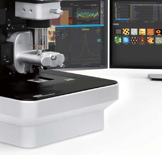

1 The most accurate and easiest to use Atomic Force Microscope

2 Park Systems Enabling Nanoscale Advances


3 The premiere choice for nanotechnology research Better data Park NX10 produces data you can trust, replicate, and publish at the highest nano resolution. It features the world s only true non-contact AFM that prolongs tip life while preserving your sample, and flexure based independent XY and Z scanner for unparalleled accuracy and resolution. Better productivity Powered by our revolutionary operating software Park SmartScan TM, Park NX10 is capable of quicker, easier setup and more optimal data collection than ever before. Park SmartScan s auto mode allows novices to quickly collect high quality nanoscale images with just three clicks of a mouse while its manual mode provides all of the functionality necessary for veterans to customize their workflow as needed. Better research With more time and better data, you can focus on doing more innovative research. And the Park NX10 s wide range of measurement modes and customizable design means it can be easily tailored to the most unique projects.


4 Innovative features for innovative work Accurate XY Scan by Crosstalk Elimination Two independent, closed-loop XY and Z flexure scanners for sample and probe tip Flat and orthogonal XY scan with low residual bow Out-of-plane motion of less than 1 nm over an entire scan range Z scanner linearity deviation of less than 0.015% over an entire scan range Accurate height measurements without any need for software processing Accurate AFM Topography with Low Noise Z Detector Sample topography measured by industry leading low noise Z detector True Sample Topography without edge overshoot or piezo creep error Accurate surface height recording, even during high-speed scanning Reduced XY scanner ringing by forward sine-scan algorithm Industry leading forward and backward scan gap of less than 0.15% Best Tip Life, Resolution and Sample Preservation by True Non-Contact Mode Industry leading Z-scanner bandwidth of more than 9 khz Fastest Z-servo speed of more than 62 mm/sec tip velocity Minimum tip wear for prolonged high-quality and high-resolution imaging Minimized sample damage or modification Immune from parameter-dependent results common in tapping imaging User Experience-Driven Software and Hardware Features Open side access for easy sample or tip exchange Easy, intuitive laser alignment with pre-aligned tip mount Easy head removal by dovetail-lock mount Direct on-axis optics for high resolution optical viewing Fast automatic tip approach to sample surface within 10 seconds Park SmartScan TM - AFM operating software versatile enough to empower both novices and power users alike toward great nanoscale research. - Auto mode: Automated image acquisition in three easy steps to determine probe setup, scan position, and scan area. - Manual mode: Opens various up scan parameters and macro/scripting support to advanced users for fine-tuned scan control. The Most Comprehensive and Extensible AFM Solution The most extensive range of SPM modes The largest number of sample measurement options The best option compatibility and upgradeability in the industry 24 bit digital electronics with three internal lock-ins, Q-control, and spring constant calibration Active temperature control of acoustic enclosure


5


6 AFM Technology Flat Orthogonal XY Scanning Without Scanner Bow Park's Crosstalk Elimination removes scanner bow, allowing flat orthogonal XY scanning regardless of scan location, scan rate, and scan size. It shows no background curvature even on flattest samples, such as an optical flat, and with various scan offsets. This provides you with a very accurate height measurement and precision nanometrology for the most challenging problems in research and engineering. Decoupled XY and Z Scanners The fundamental difference between Park and its closest competitor is in the scanner architecture. Park s unique flexure based independent XY scanner and Z scanner design allows unmatched data accuracy in nano resolution in the industry. Accurate Surface Measurement Flat sample surface as it is! Low residual bow No need for software processing (raw data) Accurate results independent of scan location nm Unprocessed raw data Less than 2 nm Industry Leading Low Noise Z Detector Our AFMs are equipped with the most effective low noise Z detectors in the field, with a noise of 0.02 nm over large bandwidth. This produces highly accurate sample topography, no edge overshoot and no need for calibration. Just one of the many ways Park NX10 saves you time and gives you better data. Z Detector (Height) Park NX Series No creep effect Accurate Sample Topography Measured by Low Noise Z Detector Uses low noise Z detector signal for topography Has low Z detector noise of 0.02 nm over large bandwidth Has no edge overshoot at the leading and trailing edges Needs calibration done only once at the factory Sample: 1.2 µm Nominal Step Height (9 µm x 1 µm, 2048 pixels x 128 lines)


7 True Non-Contact Mode True Non-Contact Mode is a scan mode unique to Park AFM systems that produces high resolution and accurate data by preventing destructive tip-sample interaction during a scan. Unlike in contact mode, where the tip touches the sample continuously during a scan, or in tapping mode, where the tip touches the sample periodically, a tip used in non-contact mode does not touch the sample. Because of this, use of non-contact mode has several key advantages. Scanning at the highest resolution throughout imaging is now possible as the tip s sharpness is maintained. Non-contact mode avoids damaging soft samples as the tip and sample surface avoid direct contact. Money is also saved as turnover on costly tips is reduced. ETD (@ 5nm) on Tip Check (nm) True Non-Contact (PPP-NCHR) Image Frame 1 st Scan 30 th Scan 70 th Scan 100 th Scan Furthermore, non-contact mode senses tip-to-sample force interactions occurring all around the tip. Forces occurring laterally to tip approach to the sample are detected. Therefore, tips used in non-contact mode can avoid crashing into tall structures that may suddenly appear on a sample surface. Contact and tapping modes only detect the force coming from below the tip and are vulnerable to such crashes. 1:1 aspect ratio Park AFM Before After taking 20 images Accurate Feedback by Faster Z-servo enables True Non-Contact AFM True Non-Contact Mode True Non-Contact Mode Less tip wear = Prolonged high-resolution scan Non-destructive tip-sample interaction = Minimized sample modification Maintains non-contact scan over a wide range of samples and conditions.


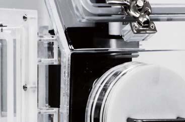
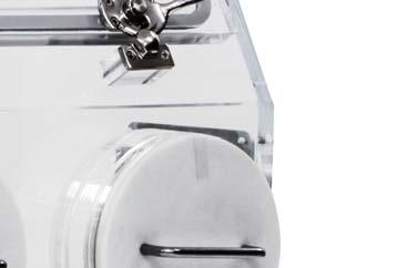
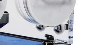
8 Equipped with the most innovative AFM technology 1 2D Flexure-Guided Scanner with 50 µm x 50 µm Scan Range The XY scanner consists of symmetrical 2-dimensional flexure and high-force piezoelectric stacks. It provides high orthogonal movement with minimal out-of-plane motion and high responsiveness that is essential for precise sample scanning in the nanometer scale. The compact and rigid structure of Park NX10 enables low noise, high-speed servo response. 2 High Speed Z Scanner with 15 µm Scan Range Driven by a high-force piezoelectric stack and guided by a flexure structure, the standard Z scanner has a high resonant frequency of more than 9 khz (typically 10.5 khz) and an ultra fast Z-servo speed of more than 48 mm/sec tip velocity. The maximum Z scan range can be extended from 15 µm to 30 µm with the optional long range Z scanner. 3 Low Noise XYZ Position Sensors The industry leading low noise Z detector replaces the applied Z voltage as the topography signal while the low noise XY closed loop scan minimizes the forward and backward scan gap to less than 0.15% of the scan range. 4 Motorized XY Sample Stage XY Sample Stage is motorized to make it easy for navigating and positioning the sample to the region of interest. This motorized stage has a resolution of 0.6um (using micro-stepping) on both axis. 5 Step-and-Scan Automation 7 9 Using the motorized sample stage, Step-and-Scan enables programmable multiple region imaging. Here s how it works: Scan an image Lift cantilever Move motorized stage to a user defined coordinate Approach Repeat scan 2 This automated feature greatly increases productivity by reducing the need for your interaction during the scan process Accessible Sample Holder The Park NX10 s unique head design handles up to 50 mm x 50 mm x 20 mm (width x length x height) sample size, and it allows easy side access to the sample and tip Expansion Slot for Advanced SPM Modes and Options Advanced SPM modes are enabled by simply plugging an option module to the expansion slot. The modular design of the NX-series AFM allows option compatibility throughout its product line.
 provides direct on-axis optical view with unprecedented clarity. This allows users to navigate the sample surface easily, and find the target area quickly.")

9 8 Direct On-Axis High Powered Optics with Integrated LED Illumination The Park NX10 s custom designed objective lens with an ultra long working distance (50 mm, WD 0.21 NA, 1.0 µm resolution) provides direct on-axis optical view with unprecedented clarity. This allows users to navigate the sample surface easily, and find the target area quickly. With the EL20x objective lens of long travel head, the enlarged sensor size of the CCD provides a resolution of 0.7 µm without losing visual quality. 9 Auto Engage by Slide-to-Connect SLD Head The AFM head is easily inserted or removed by sliding it along a dovetail rail. This automatically locks the head into its pre-aligned position and connects it to the control electronics with a positioning repeatability of a few microns. The low coherency of the Super Luminescence Diode (SLD) enables accurate imaging of highly reflective surfaces and precise measurements for pico-newton Force-distance spectroscopy. The SLD wavelength eliminates interference issues for users interested in combining the AFM with experiments in the visible spectrum. 10 Vertically Aligned Motorized Z Stage and Focus Stage The motorized Z stage and the motorized focus stage both make it possible of engaging the cantilever to the sample surface while constantly maintaining a clear vision for the user. And because the focus stage is motorized and software controlled, it has the precision necessary for transparent samples and liquid cell applications. 10 High Speed 24-bit Digital Electronics All the NX-series AFMs are controlled and processed by the same NX electronics controller. The controller is an all digital, 24-bit high speed electronics which successfully realizes the True Non-Contact mode for accuracy and speed. With its low noise design and high speed processing unit, the controller is also ideal for precise voltage and current measurement as well as nanoscale imaging. The embedded digital signal processing capability adds to the functionality and the economics of our AFM solutions for advanced researchers. 24-bit signal resolution for XY and Z detectors nm resolution in XY (50 µm XY) nm resolution in Z (15 µm Z) 3 Park NX AFM Controller Embedded digital signal processing capability 3 channels of flexible digital lock-ins Spring constant calibration (thermal method) Digital Q control included Intergrated signal access ports Dedicated and programmable signal input/output ports 7 inputs and 3 outputs Revolutionary operating software for Park AFMs combining versatility, ease-of-use, and top-flight quality performance for the best AFM experience available. Featuring an Auto mode to assist inexperienced users to quickly acquire quality nanoscale images with minimal effort, Park SmartScan also has a full Manual mode to enable AFM power users in crafting a totally customized sample scan with access to various parameters, settings, and advanced features such as macros and scripting.


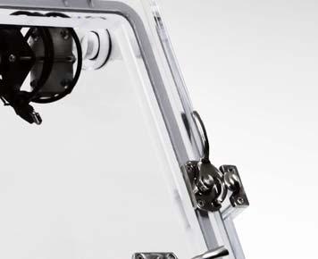
10 Why the world s most accurate small sample AFM is also the easiest to use Easy Tip and Sample Exchange The unique head design allows easy side access allowing you to easily snap new tips and samples into place by hand. The cantilever is ready for scanning without the need for any tricky laser beam alignment by using pre-aligned cantilevers mounted on to the cantilever tip holder. Easy Snap by Hand Lightning Fast Automatic Tip Approach Our automatic tip to sample approach requires no user intervention and engages in just 10 seconds after loading the cantilever. By monitoring the cantilever response to the approaching surface, Park NX10 can initiate an automatic fast tip to sample approach within 10 seconds of cantilever loading. Fast feedback by the high-speed Z scanner and low noise signal processing by the NX electronics controller enable quick engagement to the sample surface without any user intervention. It just works, minimal user involvement required. Easy, Intuitive Laser Beam Alignment With our advanced pre-aligned cantilever holder, the laser beam is focused on the cantilever upon placement. Furthermore, the natural on-axis top-down view, the only one in the industry, allows you to easily find the laser spot. Since the laser beam falls vertically on the cantilever, you can intuitively move the laser spot along the X- and Y-axis by rotating its two positioning knobs. As a result, you can easily find the laser and position it on PSPD using our beam alignment user interface. From there, all you will need is a minor adjustment to maximize the signal to start acquiring the data. The Laser beam is always focused on the cantilever upon replacement


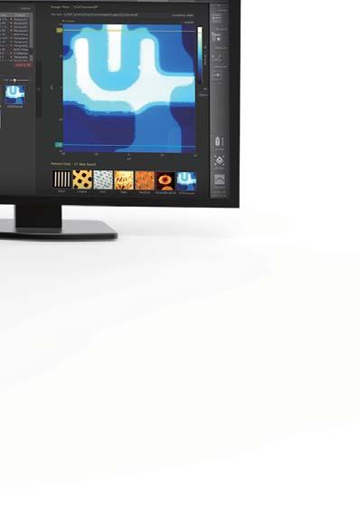
11 Quality Pixel / Scan size Speed Choose pixel density and scan size. Start with new sample A SETUP POSITION IMAGE END SETUP POSITION IMAGE END Start with new sample B Single-Click Imaging with SmartScan Auto Mode All you need to specify for AFM imaging are quality-speed preference, pixel density and scan size. Outside of those factors, you can leave all sophisticated AFM parameters up to the Auto mode of SmartScan. The system will start a measurement with optimized conditions for imaging automatically at the click of a button. An AFM OS for everyone, from amateurs to experts Whether your AFM needs are focused on academic research, industrial metrology or failure analysis, SmartScan s Auto mode offers a streamlined system to generate publishable high quality AFM data. Moreover, SmartScan promises productive sessions with an AFM even for beginners to obtain quality data as good as an expert's, in much shorter time. FastApproach Click the Position button, and the Z scanner approaches the sample automatically and at a much higher speed than the typical manual approach. Park's patented FastApproach safely takes the probe down to the sample surface at full speed without the user's intervention and engages in just 10 seconds after loading the cantilever. Easy to Find an Area of Interest After probe-to-surface engagement, the optical camera will automatically focus on the sample to find your area of interest (AOI). The UX of SmartScan easily enables intuitive navigation of the sample by controlling the motorized stages in the integrated optical window. You can move theaoi of the sample directly by clicking the desired position in the optical window. Speeds Up Imaging with AdaptiveScan Park's innovative AdaptiveScan controls the scan speed automatically based on the peaks and valleys of the sample surface. AdaptiveScan adjusts the optimum scan speed dynamically to acquire a quality image of an unknown morphology at a higher speed. This effectually shortens the imaging time while retaining top image quality comparable to that obtained by a well-trained expert manually. When moving to neighboring locations or zooming-in to a target, AdaptiveScan automatically applies a new optimal condition.
 Phase Imaging Intermittent (tapping) AFM Chemical Properties Chemical Force Microscopy with Functionalized Tip")
 Scanning Spreading-Resistance Microscopy (SSRM) Scanning Tunneling Microscopy (STM) Scanning Tunneling Spectroscopy (STS) Time-Resolved")
 Dynamic Contact EFM (DC-EFM) Piezoelectric Force Microscopy (PFM) PFM with High Voltage Mechanical Properties Force Measurement")

12 Adaptable to any project The wide range of scanning modes and modular design of the NX series allows it to be easily tailored to the needs of any scanning probe microscopy project. Standard Imaging True Non-Contact AFM Basic Contact AFM Lateral Force Microscopy (LFM) Phase Imaging Intermittent (tapping) AFM Chemical Properties Chemical Force Microscopy with Functionalized Tip Electrochemical Microscopy (EC-STM and EC-AFM) Thermal Properties Scanning Thermal Microscopy (SThM) Electrical Properties Conductive AFM I-V Spectroscopy Scanning Kelvin Probe Microscopy (SKPM/KPM) SKPM with High Voltage Scanning Capacitance Microscopy (SCM) Scanning Spreading-Resistance Microscopy (SSRM) Scanning Tunneling Microscopy (STM) Scanning Tunneling Spectroscopy (STS) Time-Resolved Photo Current Mapping (Tr-PCM) Optical Properties Tip-Enhanced Raman Spectroscopy (TERS) Time-Resolved Photo Current Mapping (Tr-PCM) Magnetic Properties Magnetic Force Microscopy (MFM) Tunable MFM Dielectric/Piezoelectric Properties Electric Force Microscopy (EFM) Dynamic Contact EFM (DC-EFM) Piezoelectric Force Microscopy (PFM) PFM with High Voltage Mechanical Properties Force Measurement Force Modulation Microscopy (FMM) Nanoindentation Nanolithography Nanolithography with High Voltage Nanomanipulation Piezoelectric Force Microscopy (PFM) Force Distance (F-D) Spectroscopy Force Volume Imaging Spring Constant Calibration by Thermal Method Tall Sample 1.5 μm step height Flat Sample Atomic steps of sapphire wafer 1 Scan Mode: Non-contact mode, Topography from Z position sensor 0.3 nm step height, Scan Mode: Non-contact mode, Topography from Z position sensor 2 Hard Sample Tungsten film Soft Sample Collagen fibril 3 Scan Mode: Non-contact mode, Topography from Z position sensor Scan Mode: Non-contact mode, Topography from Z position sensor 4

 software")


 functionality.")

 250 ºC Heating Stage 600 ºC Heating Stage Liquid Cells Universal Liquid")


13 Options Park NX10 SICM permits truly non-invasive in-liquid imaging by combining the usage of nanopipettes with a no force, non-contact technique under aqueous conditions. This approach is powered by our dedicated Approach-Retract-Scan (ARS) software that enables both steamlined scanning automation through nanoscale probe-sample distance control. Park NX10 SICM is now available for a wide range of applications ranging from cell biology, analytical chemistry, electrophysiology, and neuroscience Park NX10 SICM Module A new hardware module for the Park NX10 to enable Scanning Ion Conductance Microscopy (SICM) functionality. XY Scanners 10 µm x 10 µm XY Scanner 50 µm x 50 µm XY Scanner 100 µm x 100 µm XY Scanner Z Scanner Heads 15 µm Z Scanner Head 30 µm Z Scanner Head Wide optical access from the side Temperature Control Heating & Cooling Stage (0~180 ºC) 250 ºC Heating Stage 600 ºC Heating Stage Liquid Cells Universal Liquid Cell Electrochemistry Cell Open Liquid Cell Liquid Probehand Designed for imaging in general liquid environment Resistant to most buffer solutions including acid Contact and Non-contact AFM imaging in liquid Clip-type Chip Carrier Can be used with unmounted cantilever Tip bias function available for Conductive AFM and EFM Tip bias range: -10 V ~ 10 V Magnetic Field Generator Applies external magnetic field parallel to sample surface Tunable magnetic field Range: -300 ~ 300 gauss Composed of pure iron core & two solenoid coils Active Temperature Controlled Acoustic Enclosure Easy to use controls - Innovative control design allows Park NX10 to quickly reach temperature equilibrium Get scanning faster - Temperature stability of less than 0.05 ºC within 10 minutes of closing the Acoustic Enclosure door
14 Specification Scanner Z scanner XY scanner AFM Head Guided high-force flexure scanner Scan range: 15 µm (optional 30 µm) Resolution: nm Position detector noise: 0.03 nm (bandwidth: 1 khz) Resonant frequency: > 9 khz (typically 10.5 khz) SICM Head Flexure-guided structure driven by multiply-stacked piezoelectric stacks Z scan range: 25 µm Position detector noise: 0.03 nm (bandwidth: 1 khz) Single module flexure XY-scanner with closed-loop control Scan range: 50 µm 50 µm (optional 10 µm 10 µm or 100 µm 100 µm) Resolution: 0.05 nm Position detector noise: < 0.25 nm (bandwidth: 1 khz) Out-of-plane motion: < 2 nm (over 40 µm scan) Stage Vision Sample size: Open space up to 100 mm x 100 mm, thickness up to 20 mm Sample weight: up to 500 g XY stage travel range: 20 mm x 20 mm Z stage travel range: 25 mm Focus stage travel range: 15 mm Direct on-axis vision of sample surface and cantilever Field-of-view: 480 µm 360 µm (with 10 objective lens) CCD: 1 Mpixel (pixel resolution: 0.4 µm) 5 Mpixel (pixel resolution: 0.2 µm) Objective lens 10x (0.21NA) ultra-long working distance lens (1µm resolution) 20x (0.42 NA) high-resolution, long working distance lens (0.6 µm resolution) Electronics Signal processing Integrated functions External signal access ADC: 18 channels ADC channels (64 MSPS) 24-bit ADCs for X, Y, and Z scanner position sensor DAC: 11 channels DAC channels (64 MSPS) 20-bit DACs for X, Y, and Z scanner positioning Maximum data size: 4096 x 4096 pixels 3 channels of flexible digital lock-in amplifier Spring constant calibration (Thermal method) Digital Q control 20 embedded signal input/output ports 5 TTL outputs: EOF, EOL, EOP, Modulation, and AC bias Options/Modes Standard Imaging Chemical Properties Dielectric/Piezoelectric Properties True Non-Contact Mode Basic Contact Mode Lateral Force Microscopy (LFM) Phase Imaging Mode Tapping Mode Chemical Force Microscopy with Functionalized Tip Electrochemical Microscopy (EC-STM and EC-AFM) Electric Force Microscopy (EFM) Dynamic Contact EFM (EFM-DC) Piezoelectric Force Microscopy (PFM) PFM with High Voltage Force Measurement Force Distance (F-D) Spectroscopy Force Volume Imaging Magnetic Properties Magnetic Force Microscopy (MFM) Tunable MFM Thermal Properties Scanning Thermal Microscopy (SThM) Electrical Properties Pinpoint Conductive AFM (CP-AFM) I-V Spectroscopy Scanning Kelvin Probe Microscopy (SKPM/KPM) SKPM with High Voltage QuickStep Scanning Capacitance Microscopy (SCM) Scanning Spreading-Resistance Microscopy (SSRM) Scanning Tunneling Microscopy (STM) Scanning Tunneling Spectroscopy (STS) Photo Current Mapping (PCM) Current-Distance Spectroscopy (with SICM) Mechanical Properties Pinpoint Mode Force Modulation Microscopy (FMM) Nanoindentation Nanolithography Nanolithography with High Voltage Nanomanipulation Software Park SmartScan TM AFM system control and data acquisition software Auto mode for quick setup and easy imaging Manual mode for advanced use and finer scan control XEI AFM data analysis software Stand-alone design can install and analyze data away from AFM Capable of producing 3D renders of acquired data Accessories Electrochemistry Cell Universal Liquid Cell with Temperature Control Sample Stages with Temperature Control GloveBox Magnetic Field Generator Active Temperature Controlled Acoustic Enclosure
15 810 mm 682 mm 500 mm 625 mm Dimensions in mm GloveBox * Optional 748 mm 710 mm 245 mm 293 mm Park NX10 * Optional Acoustic Enclosure mm 630 mm 443 mm * Optional Park NX10 Full System with Acoustic Enclosure mm 700 mm 1450 mm 650 mm 650 mm 850 mm 1300 mm


16 Park Systems Dedicated to producing the most accurate and easiest to use AFMs The global headquarters is located at Korean Advanced Nanotechnology Center (KANC) in Suwon, Korea. More than a quarter century ago, the foundations for Park Systems were laid at Stanford University where Dr. Sang-il Park, the founder of Park Systems worked as an integral part of the group that first developed AFM technology. After perfecting the technology, he then went on to create the first commercial AFM and later Park Systems was born. Park Systems strives everyday to live up to the innovative spirit of its beginnings. Throughout our long history, we have honored our commitment to providing the most accurate and yet very easy to use AFMs, with revolutionary features like True Non-Contact mode, and many automated software tools. We are not simply content to rest on our past success. All of our products are designed with same care and creativity that went into our first, allowing you to focus on getting results without worrying about the integrity of your tools. HEADQUARTERS GLOBAL HEADQUARTERS: AMERICAS HEADQUARTERS: JAPAN HEADQUARTERS: SE ASIA HEADQUARTERS: OCEANIA Australia and New Zealand: ASIA China: India: Indonesia: Malaysia: Pakistan: Philippines: Saudi Arabia: Taiwan: Thailand: UAE: Vietnam: EUROPE AMERICAS France: USA: Germany: Canada: Italy: Brazil: Israel: Colombia: Switzerland: Ecuador: Romania: Chile: Russia: +7 (495) Mexico: Spain and Portugal: Turkey: UK an Ireland: +44(0) Benelux, Scandinavia, and Baltics: Note: All specifications are subject to change without notice. Please visit our website for the most up-to-date specifications.
Park NX-Hivac The world s most accurate and easy to use high vacuum AFM for failure analysis.
 Park NX-Hivac The world s most accurate and easy to use high vacuum AFM for failure analysis www.parkafm.com Park NX-Hivac High vacuum scanning for failure analysis applications 4 x 07 / Cm3 Current (µa)
Park XE7 The most affordable research grade AFM with flexible sample handling.
 Park XE7 The most affordable research grade AFM with flexible sample handling www.parkafm.com Park Systems The Most Accurate Atomic Force Microscope Park XE7 The economical choice for innovative research
The Most Accurate Atomic Force Microscope. Park NX20 The leading nano metrology tool for failure analysis and large sample research.
 The Most Accurate Atomic Force Microscope Park NX20 The leading nano metrology tool for failure analysis and large sample research www.parkafm.com Park Systems The Most Accurate Atomic Force Microscope
Park NX20 The leading nano metrology tool for failure analysis and large sample research.
 The Most Accurate Atomic Force Microscope Park NX20 The leading nano metrology tool for failure analysis and large sample research www.parkafm.com The Most Accurate Atomic Force Microscope Park NX20 The
The Most Accurate Atomic Force Microscope. Park XE15 Power and versatility, brilliantly combined.
 The Most Accurate Atomic Force Microscope Park XE15 Power and versatility, brilliantly combined. www.parkafm.com Park XE15 Increase your productivity with our powerfully versatile atomic force microscope
The World s Most Accurate AFM System. Park NX-3DM Innovation and Efficiency for 3D Metrology.
 The World s Most Accurate AFM System Park NX-3DM Innovation and Efficiency for 3D Metrology www.parkafm.com Park NX-3DM An Indispensable Tool for Wafer Fabrication A fully automated industrial AFM using
INDIAN INSTITUTE OF TECHNOLOGY BOMBAY
 IIT Bombay requests quotations for a high frequency conducting-atomic Force Microscope (c-afm) instrument to be set up as a Central Facility for a wide range of experimental requirements. The instrument
Advanced Nanoscale Metrology with AFM
 Advanced Nanoscale Metrology with AFM Sang-il Park Corp. SPM: the Key to the Nano World Initiated by the invention of STM in 1982. By G. Binnig, H. Rohrer, Ch. Gerber at IBM Zürich. Expanded by the invention
Cutting-edge Atomic Force Microscopy techniques for large and multiple samples
 Cutting-edge Atomic Force Microscopy techniques for large and multiple samples Study of up to 200 mm samples using the widest set of AFM modes Industrial standards of automation A unique combination of
SPM The Industry s Performance Leader High Resolution Closed-loop System Fast, Easy Tip & Sample Exchange Versatility and Value Powerful Research
 SPM The Industry s Performance Leader High Resolution Closed-loop System Fast, Easy Tip & Sample Exchange Versatility and Value Powerful Research Flexibility Atomic resolution STM image of highly-oriented
Nanotechnology Solutions Partner
 Nanotechnology Solutions Partner Park Systems Corp. KANC 4F, Iui-Dong 6-10, Suwon, Korea 443-270 Tel. +82-31-546-6800 Fax. +82-31-546-6805 www.parkafm.co.kr Park Systems Inc. 3040 Olcott St. Santa Clara,
Keysight Technologies 5500 AFM Controller Upgrade. Data Sheet
 Keysight Technologies 5500 AFM Controller Upgrade Data Sheet 02 Keysight 5500 AFM Controller Upgrade - Data Sheet Upgrade Overview The Keysight 5500 AFM Controller Upgrade offers a tremendously convenient
Nanosurf easyscan 2 FlexAFM
 Nanosurf easyscan 2 FlexAFM Your Versatile AFM System for Materials and Life Science www.nanosurf.com The new Nanosurf easyscan 2 FlexAFM scan head makes measurements in liquid as simple as measuring in
Keysight 9500 AFM. Data Sheet
 Keysight 9500 AFM Data Sheet System Overview The Keysight Technologies, Inc. 9500 AFM seamlessly integrates revolutionary new software, a new high-bandwidth digital controller, and a state-of-the-art mechanical
Standard Operating Procedure of Atomic Force Microscope (Anasys afm+)
") Standard Operating Procedure of Atomic Force Microscope (Anasys afm+) The Anasys Instruments afm+ system incorporates an Atomic Force Microscope which can scan the sample in the contact mode and generate
Standard Operating Procedure of Atomic Force Microscope (Anasys afm+) The Anasys Instruments afm+ system incorporates an Atomic Force Microscope which can scan the sample in the contact mode and generate
Ionscope SICM. About Ionscope. Scanning Ion Conductance Microscopy. Ionscope A brand of Openiolabs Limited
 SICM About is a brand of openiolabs Ltd, headquartered in Cambridge UK, is the world-leader in (SICM), a rapidly emerging Scanning Probe Microscopy (SPM) technique which allows nanoscale topographical
nanovea.com PROFILOMETERS 3D Non Contact Metrology
 PROFILOMETERS 3D Non Contact Metrology nanovea.com PROFILOMETER INTRO Nanovea 3D Non-Contact Profilometers are designed with leading edge optical pens using superior white light axial chromatism. Nano
Nanonics Systems are the Only SPMs that Allow for On-line Integration with Standard MicroRaman Geometries
 Nanonics Systems are the Only SPMs that Allow for On-line Integration with Standard MicroRaman Geometries 2002 Photonics Circle of Excellence Award PLC Ltd, England, a premier provider of Raman microspectral
Optical Microscope. Active anti-vibration table. Mechanical Head. Computer and Software. Acoustic/Electrical Shield Enclosure
 Optical Microscope On-axis optical view with max. X magnification Motorized zoom and focus Max Field of view: mm x mm (depends on zoom) Resolution : um Working Distance : mm Magnification : max. X Zoom
Indian Institute of Technology Bombay
 Specifications for High Resolution Scanning Probe Microscope Item Essential measuring modes with complete hardware and software. All the modes should be demonstrated during installation & training Scanners
Keysight Technologies Scanning Microwave Microscope Mode. Application Note
 Keysight Technologies Scanning Microwave Microscope Mode Application Note Introduction Measuring electromagnetic properties of materials can provide insight into applications in many areas of science and
Thermo Scientific SPECTRONIC 200 Education
 molecular spectroscopy Thermo Scientific SPECTRONIC 200 Education Part of Thermo Fisher Scientific Designed for the Teaching Laboratory Classroom Friendly Sample Compartment Whether you measure in 10 mm
Microscopic Structures
 Microscopic Structures Image Analysis Metal, 3D Image (Red-Green) The microscopic methods range from dark field / bright field microscopy through polarisation- and inverse microscopy to techniques like
Scanning Ion Conductance Microscope ICnano
 Sperm Cell Epithelial Cells I nner Ear Hair Cells I nner Ear Hair Cell Neurons E- Coli Bac teria Scanning Ion Conductance Microscope ICnano About ionscope About ionscope The ionscope scanning ion conductance
Thermo Scientific SPECTRONIC 200
 molecular spectroscopy Thermo Scientific SPECTRONIC 200 Part of Thermo Fisher Scientific The New Standard for Routine Measurements Robust, Multifunction Sample Compartment Whether you measure in 10 mm
Keysight Technologies Why Magnification is Irrelevant in Modern Scanning Electron Microscopes. Application Note
 Keysight Technologies Why Magnification is Irrelevant in Modern Scanning Electron Microscopes Application Note Introduction From its earliest inception, the Scanning Electron Microscope (SEM) has been
MEASUREMENT APPLICATION GUIDE OUTER/INNER
 MEASUREMENT APPLICATION GUIDE OUTER/INNER DIAMETER Measurement I N D E X y Selection Guide P.2 y Measurement Principle P.3 y P.4 y X and Y Axes Synchronous Outer Diameter Measurement P.5 y of a Large Diameter
Investigate in magnetic micro and nano structures by Magnetic Force Microscopy (MFM)
") Investigate in magnetic micro and nano 5.3.85- Related Topics Magnetic Forces, Magnetic Force Microscopy (MFM), phase contrast imaging, vibration amplitude, resonance shift, force Principle Caution! -
Investigate in magnetic micro and nano 5.3.85- Related Topics Magnetic Forces, Magnetic Force Microscopy (MFM), phase contrast imaging, vibration amplitude, resonance shift, force Principle Caution! -
Prepare Sample 3.1. Place Sample in Stage. Replace Probe (optional) Align Laser 3.2. Probe Approach 3.3. Optimize Feedback 3.4. Scan Sample 3.
 Align Laser 3.2. Probe Approach 3.3. Optimize Feedback 3.4. Scan Sample 3.") CHAPTER 3 Measuring AFM Images Learning to operate an AFM well enough to get an image usually takes a few hours of instruction and practice. It takes 5 to 10 minutes to measure an image if the sample is
CHAPTER 3 Measuring AFM Images Learning to operate an AFM well enough to get an image usually takes a few hours of instruction and practice. It takes 5 to 10 minutes to measure an image if the sample is
Thermo Scientific SPECTRONIC 200 Visible Spectrophotometer. The perfect tool. for routine measurements
 Thermo Scientific SPECTRONIC 200 Visible Spectrophotometer The perfect tool for routine measurements The Standard for Routine Measurements Thermo Scientific SPECTRONIC spectrophotometers have served as
Measurement of Microscopic Three-dimensional Profiles with High Accuracy and Simple Operation
 238 Hitachi Review Vol. 65 (2016), No. 7 Featured Articles Measurement of Microscopic Three-dimensional Profiles with High Accuracy and Simple Operation AFM5500M Scanning Probe Microscope Satoshi Hasumura
Atomic Force Microscopy (Bruker MultiMode Nanoscope IIIA)
") Atomic Force Microscopy (Bruker MultiMode Nanoscope IIIA) This operating procedure intends to provide guidance for general measurements with the AFM. For more advanced measurements or measurements with
Atomic Force Microscopy (Bruker MultiMode Nanoscope IIIA) This operating procedure intends to provide guidance for general measurements with the AFM. For more advanced measurements or measurements with
Lecture 20: Optical Tools for MEMS Imaging
 MECH 466 Microelectromechanical Systems University of Victoria Dept. of Mechanical Engineering Lecture 20: Optical Tools for MEMS Imaging 1 Overview Optical Microscopes Video Microscopes Scanning Electron
Thermo Scientific SPECTRONIC 200 Visible Spectrophotometer. The perfect. teaching instrument
 Thermo Scientific SPECTRONIC 200 Visible Spectrophotometer The perfect teaching instrument Designed for the Teaching Laboratory Thermo Scientific SPECTRONIC spectrophotometers have served as core analytical
Introduction of New Products
 Field Emission Electron Microscope JEM-3100F For evaluation of materials in the fields of nanoscience and nanomaterials science, TEM is required to provide resolution and analytical capabilities that can
PicoMaster 100. Unprecedented finesse in creating 3D micro structures. UV direct laser writer for maskless lithography
 UV direct laser writer for maskless lithography Unprecedented finesse in creating 3D micro structures Highest resolution in the market utilizing a 405 nm diode laser Structures as small as 300 nm 375 nm
- Near Field Scanning Optical Microscopy - Electrostatic Force Microscopy - Magnetic Force Microscopy
 - Near Field Scanning Optical Microscopy - Electrostatic Force Microscopy - Magnetic Force Microscopy Yongho Seo Near-field Photonics Group Leader Wonho Jhe Director School of Physics and Center for Near-field
Manufacturing Metrology Team
 The Team has a range of state-of-the-art equipment for the measurement of surface texture and form. We are happy to discuss potential measurement issues and collaborative research Manufacturing Metrology
NanoFocus Inc. Next Generation Scanning Probe Technology. Tel : Fax:
 NanoFocus Inc. Next Generation Scanning Probe Technology www.nanofocus.kr Tel : 82-2-864-3955 Fax: 82-2-864-3956 Albatross SPM is Multi functional research grade system Flexure scanner and closed-loop
Nanosurf Nanite. Automated AFM for Industry & Research.
 Nanosurf Nanite Automated AFM for Industry & Research www.nanosurf.com Multiple Measurements Automated Got work? Nanosurf has the solution! The Swiss-based innovator and manufacturer of the most compact
Fiber Optic Device Manufacturing
 Precision Motion Control for Fiber Optic Device Manufacturing Aerotech Overview Accuracy Error (µm) 3 2 1 0-1 -2 80-3 40 0-40 Position (mm) -80-80 80 40 0-40 Position (mm) Single-source supplier for precision
UNIVERSITY OF WATERLOO Physics 360/460 Experiment #2 ATOMIC FORCE MICROSCOPY
 UNIVERSITY OF WATERLOO Physics 360/460 Experiment #2 ATOMIC FORCE MICROSCOPY References: http://virlab.virginia.edu/vl/home.htm (University of Virginia virtual lab. Click on the AFM link) An atomic force
Basic methods in imaging of micro and nano structures with atomic force microscopy (AFM)
") Basic methods in imaging of micro and nano P2538000 AFM Theory The basic principle of AFM is very simple. The AFM detects the force interaction between a sample and a very tiny tip (
Basic methods in imaging of micro and nano P2538000 AFM Theory The basic principle of AFM is very simple. The AFM detects the force interaction between a sample and a very tiny tip (
PICO MASTER 200. UV direct laser writer for maskless lithography
 PICO MASTER 200 UV direct laser writer for maskless lithography 4PICO B.V. Jan Tinbergenstraat 4b 5491 DC Sint-Oedenrode The Netherlands Tel: +31 413 490708 WWW.4PICO.NL 1. Introduction The PicoMaster
Bruker Dimension Icon AFM Quick User s Guide
 Bruker Dimension Icon AFM Quick User s Guide August 8 2014 GLA Contacts Jingjing Jiang (jjiang2@caltech.edu 626-616-6357) Xinghao Zhou (xzzhou@caltech.edu 626-375-0855) Bruker Tech Support (AFMSupport@bruker-nano.com
Bruker Dimension Icon AFM Quick User s Guide
 Bruker Dimension Icon AFM Quick User s Guide March 3, 2015 GLA Contacts Jingjing Jiang (jjiang2@caltech.edu 626-616-6357) Xinghao Zhou (xzzhou@caltech.edu 626-375-0855) Bruker Tech Support (AFMSupport@bruker-nano.com
Bringing Answers to the Surface
 3D Bringing Answers to the Surface 1 Expanding the Boundaries of Laser Microscopy Measurements and images you can count on. Every time. LEXT OLS4100 Widely used in quality control, research, and development
Keysight Technologies Using Non-Contact AFM to Image Liquid Topographies. Application Note
 Keysight Technologies Using Non-Contact AFM to Image Liquid Topographies Application Note Introduction High resolution images of patterned liquid surfaces have been acquired without inducing either capillary
LOW TEMPERATURE STM/AFM
 * CreaTec STM of Au(111) using a CO-terminated tip, 20mV bias, 0.6nA* LOW TEMPERATURE STM/AFM High end atomic imaging, spectroscopy and manipulation Designed and manufactured in Germany by CreaTec Fischer
Scanning Microwave. Expanding Impedance Measurements to the Nanoscale: Coupling the Power of Scanning Probe Microscopy with the PNA
 Agilent Technologies Scanning Microwave Microscopy (SMM) Expanding Impedance Measurements to the Nanoscale: Coupling the Power of Scanning Probe Microscopy with the PNA Presented by: Craig Wall PhD Product
IN-SIGHT 9902L LINE SCAN VISION SYSTEM
 IN-SIGHT 9902L LINE SCAN VISION SYSTEM The In-Sight 9902L 2K line scan smart camera is a high resolution self-contained vision system ideal for detailed inspections of large, cylindrical, or continuously
contents TABLE OF The SECOM platform Applications - sections Applications - whole cells Features Integrated workflow Automated overlay
 S E C O M TABLE OF contents The SECOM platform 4 Applications - sections 5 Applications - whole cells 8 Features 9 Integrated workflow 12 Automated overlay ODEMIS - integrated software Specifications 13
Comparison of resolution specifications for micro- and nanometer measurement techniques
 P4.5 Comparison of resolution specifications for micro- and nanometer measurement techniques Weckenmann/Albert, Tan/Özgür, Shaw/Laura, Zschiegner/Nils Chair Quality Management and Manufacturing Metrology
Automated Frequency Response Measurement with AFG31000, MDO3000 and TekBench Instrument Control Software APPLICATION NOTE
 Automated Frequency Response Measurement with AFG31000, MDO3000 and TekBench Instrument Control Software Introduction For undergraduate students in colleges and universities, frequency response testing
Outline: Introduction: What is SPM, history STM AFM Image treatment Advanced SPM techniques Applications in semiconductor research and industry
 1 Outline: Introduction: What is SPM, history STM AFM Image treatment Advanced SPM techniques Applications in semiconductor research and industry 2 Back to our solutions: The main problem: How to get nm
Asylum Research. MFP-3D Infinity. Endless Applications. Unlimited Potential. Performance / Versatility / Support
 MFP-3D Infinity AFM Asylum Research Endless Applications. Unlimited Potential. Performance / Versatility / Support MFP-3D Infinity AFM Asylum Research Endless applications. Unlimited potential. The Asylum
ATOMIC FORCE MICROSCOPY
 B47 Physikalisches Praktikum für Fortgeschrittene Supervision: Prof. Dr. Sabine Maier sabine.maier@physik.uni-erlangen.de ATOMIC FORCE MICROSCOPY Version: E1.4 first edit: 15/09/2015 last edit: 05/10/2018
ABB Oy, KPM. Sakeusmittaukset paperikoneen massanvalmistuksessa
 ABB Oy, KPM Sakeusmittaukset paperikoneen massanvalmistuksessa KPM Kajaani Process Measurements Ltd. KPM was established 2001 KPM was acquired by ABB on 2011, now Worldwide Sales and Service Network Researh
Systematic Workflow via Intuitive GUI. Easy operation accomplishes your goals faster than ever.
 Systematic Workflow via Intuitive GUI Easy operation accomplishes your goals faster than ever. 16 With the LEXT OLS4100, observation or measurement begins immediately once the sample is placed on the stage.
Fastest high definition Raman imaging. Fastest Laser Raman Microscope RAMAN
 Fastest high definition Raman imaging Fastest Laser Raman Microscope RAMAN - 11 www.nanophoton.jp Observation A New Generation in Raman Observation RAMAN-11 developed by Nanophoton was newly created by
10 Things to Consider when Acquiring a Nanopositioning System
 10 Things to Consider when Acquiring a Nanopositioning System There are many factors to consider when looking for nanopositioning piezo stages. This article will help explain some items that are important
Super High Vertical Resolution Non-Contact 3D Surface Profiler BW-S500/BW-D500 Series
 Super High Vertical Resolution Non-Contact 3D Surface Profiler BW-S500/BW-D500 Series Nikon's proprietary scanning-type optical interference measurement technology achieves 1pm* height resolution. * Height
SOURCE MEASURE UNITS. Make Multiple Measurements Accurately Using a Single Instrument All While Saving Space, Time and Money
 SOURCE MEASURE UNITS Make Multiple Measurements Accurately Using a Single Instrument All While Saving Space, Time and Money Do you use a power supply or digital multimeter? How about an electronic load,
Difrotec Product & Services. Ultra high accuracy interferometry & custom optical solutions
 Difrotec Product & Services Ultra high accuracy interferometry & custom optical solutions Content 1. Overview 2. Interferometer D7 3. Benefits 4. Measurements 5. Specifications 6. Applications 7. Cases
Improving the Collection Efficiency of Raman Scattering
 PERFORMANCE Unparalleled signal-to-noise ratio with diffraction-limited spectral and imaging resolution Deep-cooled CCD with excelon sensor technology Aberration-free optical design for uniform high resolution
Options and Accessories for Asylum Research MFP-3D AFMs
 ACCESSORIES Options and Accessories for Asylum Research MFP-3D AFMs Empower your research with powerful, innovative new capabilities Go beyond topography with advanced modes and environmental control Powerful
PFM Experiments with High Voltage DC/AC Bias
 PFM Experiments with High Voltage DC/AC Bias Support Note Shijie Wu and John Alexander Agilent Technologies Introduction Piezoelectric force microscopy (PFM) has found major applications in the study of
Measuring CNT FETs and CNT SETs Using the Agilent B1500A
 Measuring CNT FETs and CNT SETs Using the Agilent B1500A Application Note B1500-1 Agilent B1500A Semiconductor Device Analyzer Introduction Exotic carbon nanotube (CNT) structures have generated a great
MEMS for RF, Micro Optics and Scanning Probe Nanotechnology Applications
 MEMS for RF, Micro Optics and Scanning Probe Nanotechnology Applications Part I: RF Applications Introductions and Motivations What are RF MEMS? Example Devices RFIC RFIC consists of Active components
Fast Laser Raman Microscope RAMAN
 Fast Laser Raman Microscope RAMAN - 11 www.nanophoton.jp Fast Raman Imaging A New Generation of Raman Microscope RAMAN-11 developed by Nanophoton was created by combining confocal laser microscope technology
Standard Operating Procedure
 Standard Operating Procedure Nanosurf Atomic Force Microscopy Operation Facility NCCRD Nanotechnology Center for Collaborative Research and Development Department of Chemistry and Engineering Physics The
Camera Overview. Digital Microscope Cameras for Material Science: Clear Images, Precise Analysis. Digital Cameras for Microscopy
 Digital Cameras for Microscopy Camera Overview For Materials Science Microscopes Digital Microscope Cameras for Material Science: Clear Images, Precise Analysis Passionate about Imaging: Olympus Digital
OPTICS IN MOTION. Introduction: Competing Technologies: 1 of 6 3/18/2012 6:27 PM.
 1 of 6 3/18/2012 6:27 PM OPTICS IN MOTION STANDARD AND CUSTOM FAST STEERING MIRRORS Home Products Contact Tutorial Navigate Our Site 1) Laser Beam Stabilization to design and build a custom 3.5 x 5 inch,
Practical work no. 3: Confocal Live Cell Microscopy
 Practical work no. 3: Confocal Live Cell Microscopy Course Instructor: Mikko Liljeström (MIU) 1 Background Confocal microscopy: The main idea behind confocality is that it suppresses the signal outside
Camera Overview. Digital Microscope Cameras for Material Science: Clear Images, Precise Analysis. Digital Cameras for Microscopy
 Digital Cameras for Microscopy Camera Overview For Materials Science Microscopes Digital Microscope Cameras for Material Science: Clear Images, Precise Analysis Passionate about Imaging: Olympus Digital
attocube systems Probe Stations for Extreme Environments CRYOGENIC PROBE STATION fundamentals principles of cryogenic probe stations
 PAGE 88 & 2008 2007 PRODUCT CATALOG CRYOGENIC PROBE STATION fundamentals...................... 90 principles of cryogenic probe stations attocps I.......................... 92 ultra stable cryogenic probe
Nikon. King s College London. Imaging Centre. N-SIM guide NIKON IMAGING KING S COLLEGE LONDON
 N-SIM guide NIKON IMAGING CENTRE @ KING S COLLEGE LONDON Starting-up / Shut-down The NSIM hardware is calibrated after system warm-up occurs. It is recommended that you turn-on the system for at least
Add CLUE to your SEM. High-efficiency CL signal-collection. Designed for your SEM and application. Maintains original SEM functionality
 Add CLUE to your SEM Designed for your SEM and application The CLUE family offers dedicated CL systems for imaging and spectroscopic analysis suitable for most SEMs. In addition, when combined with other
Synergy ESPM 3-D Environmental Scanning Probe Microscope Operation Manual
 Synergy ESPM 3-D Environmental Scanning Probe Microscope Operation Manual Manufactured in the USA Rev. 01/2005 1. Introduction What Is Atomic Force Microscopy? 3 2. Getting Started Introduction 4 What
University of MN, Minnesota Nano Center Standard Operating Procedure
 Equipment Name: Atomic Force Microscope Badger name: afm DI5000 PAN Revisionist Paul Kimani Model: Dimension 5000 Date: October 6, 2017 Location: Bay 1 PAN Revision: 1 A. Description i. Enhanced Motorized
DATAMAN 470 SERIES BARCODE READERS. Premium fixed-mount barcode readers for the most challenging applications
 DATAMAN 470 SERIES BARCODE READERS Premium fixed-mount barcode readers for the most challenging applications DATAMAN 470 SERIES BARCODE READERS Premium fixed-mount barcode readers for the most challenging
Instructions for the Experiment
 Instructions for the Experiment Excitonic States in Atomically Thin Semiconductors 1. Introduction Alongside with electrical measurements, optical measurements are an indispensable tool for the study of
Park NX-Hivac: Phase-lock Loop for Frequency Modulation Non-Contact AFM
 Park Atomic Force Microscopy Application note #21 www.parkafm.com Hosung Seo, Dan Goo and Gordon Jung, Park Systems Corporation Romain Stomp and James Wei Zurich Instruments Park NX-Hivac: Phase-lock Loop
Unit-25 Scanning Tunneling Microscope (STM)
") Unit-5 Scanning Tunneling Microscope (STM) Objective: Imaging formation of scanning tunneling microscope (STM) is due to tunneling effect of quantum physics, which is in nano scale. This experiment shows
Unit-5 Scanning Tunneling Microscope (STM) Objective: Imaging formation of scanning tunneling microscope (STM) is due to tunneling effect of quantum physics, which is in nano scale. This experiment shows
Using Optics to Optimize Your Machine Vision Application
 Expert Guide Using Optics to Optimize Your Machine Vision Application Introduction The lens is responsible for creating sufficient image quality to enable the vision system to extract the desired information
AVL X-ion. Adapts. Acquires. Inspires.
 AVL X-ion Adapts. Acquires. Inspires. THE CHALLENGE Facing ever more stringent emissions targets, the quest for an efficient and affordable powertrain leads invariably through complexity. On the one hand,
Nanoscale Material Characterization with Differential Interferometric Atomic Force Microscopy
 Nanoscale Material Characterization with Differential Interferometric Atomic Force Microscopy F. Sarioglu, M. Liu, K. Vijayraghavan, A. Gellineau, O. Solgaard E. L. Ginzton Laboratory University Tip-sample
Isolation Addresses Common Sources of Differential Measurement Error
 By Tom Neville A typical measurement system includes an oscilloscope and an oscilloscope probe that provides the connection between the device under test (DUT) and the oscilloscope. Probe selection is
M-041 M-044 Tip/Tilt Stage
 M-041 M-044 Tip/Tilt Stage Piezo Drive Option for Nanometer Precision Ordering Information Linear Actuators & Motors M-041.00 Small Tilt Stage, Manual Micrometer Drive M-041.D01 Small Tilt Stage, DC-Motor
attosnom I: Topography and Force Images NANOSCOPY APPLICATION NOTE M06 RELATED PRODUCTS G
 APPLICATION NOTE M06 attosnom I: Topography and Force Images Scanning near-field optical microscopy is the outstanding technique to simultaneously measure the topography and the optical contrast of a sample.
Process Control Calibration Made Easy with Agilent U1401A
 Process Control Calibration Made Easy with Agilent U1401A Application Note This application note explains how the Agilent U1401A with simultaneous source and measure functions eases technicians calibration
TriVista. Universal Raman Solution
 TriVista Universal Raman Solution Why choose the Princeton Instruments/Acton TriVista? Overview Raman Spectroscopy systems can be derived from several dispersive components depending on the level of performance
FemtoFAB. Femtosecond laser micromachining system. tel fax Konstitucijos ave. 23C LT Vilnius, Lithuania
 FemtoFAB Femtosecond laser micromachining system Konstitucijos ave. 23C LT-08105 Vilnius, Lithuania tel. +370 5 272 57 38 fax +370 5 272 37 04 info@wophotonics.com www.wophotonics.com INTRODUCTION FemtoFAB
Ion Beam Lithography next generation nanofabrication
 Ion Beam Lithography next generation nanofabrication EFUG Bordeaux 2011 ion beams develop Lloyd Peto IBL sales manager Copyright 2011 by Raith GmbH ionline new capabilities You can now Apply an ion beam
High-impedance Buffer Amplifier System
 High-impedance Buffer Amplifier System TCA-1MEG Data Sheet Features & Benefits Bandwidth - DC to 500 MHz Input Impedance - 1 MΩ /10pF Bandwidth Limiting - Full/100 MHz/20 MHz Input Coupling - DC/AC/GND
Ultra-Broadband Forum September 2015 Madrid, Spain
 Ultra-Broadband Forum 2015 8-9 September 2015 Madrid, Spain Ovum s Global Broadband Experience Scorecard Mark Newman, Chief Research Officer, Ovum mark.newman@ovum.com Introducing Ovum s Global Broadband
Agilent 81600B All-band Tunable Laser Source Technical Specifications December 2002
 Agilent 81600B All-band Tunable Laser Source December 2002 The 81600B, the flagship product in Agilent s market-leading portfolio of tunable laser sources, sweeps the entire S, C and L- bands with just
Agilent Technologies Scanning Probe Microscope. User s Guide. Agilent Technologies
 Agilent Technologies 5500 Scanning Probe Microscope User s Guide Agilent Technologies Notices Agilent Technologies, Inc. 2008 No part of this manual may be reproduced in any form or by any means (including
Confocal imaging on the Leica TCS SP8. 1) Turn the system on. 2) Use TCS user account. 3) Start LAS X software:
 Turn the system on. 2) Use TCS user account. 3) Start LAS X software:") Confocal imaging on the Leica TCS SP8 1) Turn the system on. 2) Use TCS user account. 3) Start LAS X software: 4) Do not touch the microscope while the software is initializing. Choose your options: Turn
Confocal imaging on the Leica TCS SP8 1) Turn the system on. 2) Use TCS user account. 3) Start LAS X software: 4) Do not touch the microscope while the software is initializing. Choose your options: Turn