How to Build an LED Projector
|
|
|
- Britton Osborne
- 5 years ago
- Views:
Transcription
1 How to Build an LED Projector


")


2 SLEDS Project Organization Overview Design/Grow SLEDS (UIowa & Teledyne) Test/Optimize discrete SLEDS devices (U Iowa) Develop CMOS Drivers & Process, Package, Test Arrays (U Delaware) Develop Thermal Models for Array (ATEC) (Nova Sensors) Test SLEDS Arrays (KHILS)


3 SLEDS System Description Part 1 Emitter Array Silicon RIIC Hybrid Array Packaged 512x512 Array 512x512, 48mm-pitch, 1-color MWIR SLEDS array Packaged in liquid nitrogen Dewar connected to CSE and tested at KHILS Semiconductor-based SLEDS are capable of higher apparent temperatures & frame rates compared to TPAs, enabling emulation of hot, highly dynamic scenes
4 Y Decoders Read In Integrated Circuit (RIIC) Overview 9 X Decoders 9 Pixel Array Pixel Array 4 Analog Inputs Pixel Array Pixel Array
5 Y Decoders Decoders Used to select the specific pixel to draw to Domino logic X Decoders Pixel Array Pixel Array 4 Pixel Array Pixel Array
6 Driver Circuits
7 Domino Logic Decoders
8 Combined Driver and Decoder Circuits


 RIIC Designed to")
 Must")
9 Emitter Array and CMOS Pixel STM Cross Sectional Image of InAs/GaSb SLEDS Superlattice UIowa MBE Lab Gen20 RIIC Single Pixel Layout SLEDS Fabricated using nanostructured InAs/GaSb superlattices, requiring precision growth by Molecular Beam Epitaxy (MBE) RIIC Designed to provide current and voltage swings required by SLEDS Close Support Electronics (CSE) Must provide 1kHz frame rate for SLEDS IRSP
10 Original Pixel Circuit X Bar Y Bar 10V X Bar Monitor Y Bar X Y
11 CMOS Pixel Advances Two color LEDs Snap Shot mode Drive strength control

12

13 Two Color CMOS Pixel

14 Two Color CMOS Pixel With Analog Memory

15 Pixel Array Zoomed Out

16 Pixel Array Even More Zoomed Out
17 Power Considerations Each pixel in a SLED array at full power dissipates 12 volts and 15 milliamps. If all pixels in a 512 by 512 array were turned on, the array would dissipate 47 kw!
18 Total Radiance (arb.units) Thermal Problems for Performance Diameter Spot KHILS Exp.Data h = 50 W/m2/K No Thermal DVI Counts
19 Current Bonded Composite Substrate (BCS) Structure 2 mil GaSb SLEDs array => 5 micron indium posts with epoxy => 10 mil silicon CMOS RIIC => 1.5 mil epoxy with dielectric spheres => 5 mil stressor => 1.5 mil epoxy with dielectric spheres => 10 mil silicon wafer => 1.5 mil epoxy with dielectric spheres => Thermal Conductivities Material Thermal Cond. [W / m*k] Silicon 130 GaSb 32 Indium 82 Molebdenum 138 Unfilled Epoxy 0.15 Filled Epoxy 1 to 1.4 Heat sink => Semiconductor Thermal Conductivities from
20 Use a High Thermal Conductivity Epoxy - BN filled epoxy can have a thermal conductivity in the 1 to 1.4 W/mK. [1] - Requires heavy loading of the epoxy with the high thermal conductivity filler. - Careful epoxy dispense needed to get a thin void-free glue line. High thermal conductivity epoxy 1-3M TC-2810 BN filled epoxy- Conductive-Epoxy-Adhesive-TC-2810?N= &&Nr=AND%28hrcy_id%3A6VHXX34PP0gs_NB1DMCTNL4_N2RL3FHWVK_GPD0K8BC31gv%29&rt=d
21 Eliminate Two of the Three Epoxy Joints 2 mil GaSb SLEDs array => 5 micron indium posts with epoxy => 10 mil silicon CMOS RIIC => High thermal conductivity epoxy => Metal heat sink => Coefficient of thermal expansion of GaSb = 7.75 e-6 O C -1 - In cooling a one cm square GaSb chip from 300K to 80K results in the chip getting 17 um smaller. Coefficient of thermal expansion of silicon= 2.6 e-6 O C -1 Coefficient of thermal expansion of molybdenum = 5 e-6 O C -1
22 Replace the Epoxy Joints with a Solder Joints - Two soldering steps are needed. - BCS joints need to be done at the wafer level, before indium bumps are fabricated. - Bottom solder joint gets made after hybridization. - Builds more stress into the structure. - Layers lock together at the solder s freezing temperature - Maintaining flatness may be a challenge Solder joints
23 Reflow Method CTE Stack Up CTE 2 mil GaSb SLEDs array => 5 micron indium posts with epoxy => 10 mil silicon CMOS RIIC => C C C -1 Solder => Thermal Block CuW => C -1


24 SLEDS Phase 2 Efforts 512x512 SLEDS Mounted In Dewar Sparse Grid Patterns Operability Map First demonstration of a hybridized 512x512 MWIR LED array Three quadrants with > 99% operability; one with > 89% operability - etching nonuniformity, which has been corrected Identified modest CSE electronics improvements to reach 100Hz Identified CSE and RIIC improvements to reach 1KHz

25 SLEDs Projector

26 SLEDS Projector Single color Original pixel circuit Notice the inability to draw light spots

27 Close Support Electronics

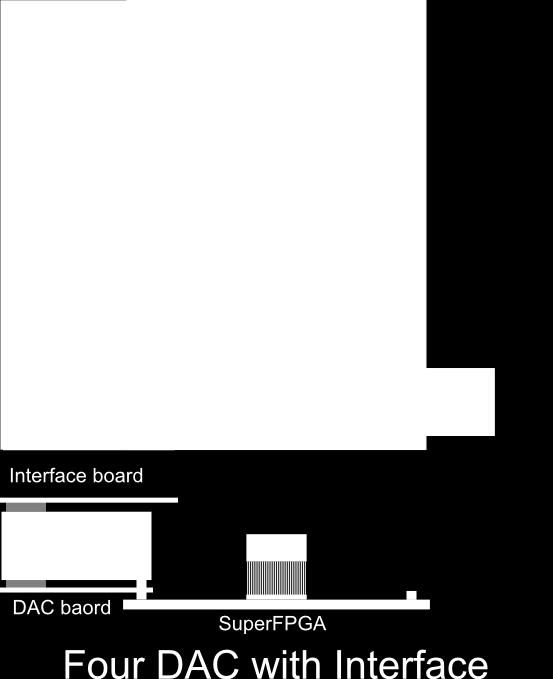
28 Interface Board Layout

29 DAC Board Layout

30 Close Support Electronics

31 Close Support Electronics
Ultra High Temperature Emitter Pixel Development for Scene Projectors
 Ultra High Temperature Emitter Pixel Development for Scene Projectors Kevin Sparkman a, Joe LaVeigne a, Steve McHugh a John Lannon b, Scott Goodwin b a Santa Barbara Infrared, Inc., 30 S. Calle Cesar Chavez,
Enhanced LWIR NUC Using an Uncooled Microbolometer Camera
 Enhanced LWIR NUC Using an Uncooled Microbolometer Camera Joe LaVeigne a, Greg Franks a, Kevin Sparkman a, Marcus Prewarski a, Brian Nehring a a Santa Barbara Infrared, Inc., 30 S. Calle Cesar Chavez,
Application Note 5026
 Surface Laminar Circuit (SLC) Ball Grid Array (BGA) Eutectic Surface Mount Assembly Application Note 5026 Introduction This document outlines the design and assembly guidelines for surface laminar circuitry
High efficient heat dissipation on printed circuit boards
 High efficient heat dissipation on printed circuit boards Figure 1: Heat flux in a PCB Markus Wille Schoeller Electronics Systems GmbH www.schoeller-electronics.com Abstract This paper describes various
Application Bulletin 240
 Application Bulletin 240 Design Consideration CUSTOM CAPABILITIES Standard PC board fabrication flexibility allows for various component orientations, mounting features, and interconnect schemes. The starting
B. Flip-Chip Technology
 B. Flip-Chip Technology B1. Level 1. Introduction to Flip-Chip techniques B1.1 Why flip-chip? In the development of packaging of electronics the aim is to lower cost, increase the packaging density, improve
LWIR NUC Using an Uncooled Microbolometer Camera
 LWIR NUC Using an Uncooled Microbolometer Camera Joe LaVeigne a, Greg Franks a, Kevin Sparkman a, Marcus Prewarski a, Brian Nehring a, Steve McHugh a a Santa Barbara Infrared, Inc., 30 S. Calle Cesar Chavez,
What the Designer needs to know
 White Paper on soldering QFN packages to electronic assemblies. Brian J. Leach VP of Sales and Marketing AccuSpec Electronics, LLC Defect free QFN Assembly What the Designer needs to know QFN Description:
64 Channel Flip-Chip Mounted Selectively Oxidized GaAs VCSEL Array
 64 Channel Flip-Chip Mounted Selectively Oxidized GaAs VCSEL Array 69 64 Channel Flip-Chip Mounted Selectively Oxidized GaAs VCSEL Array Roland Jäger and Christian Jung We have designed and fabricated
High Efficient Heat Dissipation on Printed Circuit Boards. Markus Wille, R&D Manager, Schoeller Electronics Systems GmbH
 High Efficient Heat Dissipation on Printed Circuit Boards Markus Wille, R&D Manager, Schoeller Electronics Systems GmbH m.wille@se-pcb.de Introduction 2 Heat Flux: Q x y Q z The substrate (insulation)
Micro-sensors - what happens when you make "classical" devices "small": MEMS devices and integrated bolometric IR detectors
 Micro-sensors - what happens when you make "classical" devices "small": MEMS devices and integrated bolometric IR detectors Dean P. Neikirk 1 MURI bio-ir sensors kick-off 6/16/98 Where are the targets
Thermal Management in the 3D-SiP World of the Future
 Thermal Management in the 3D-SiP World of the Future Presented by W. R. Bottoms March 181 th, 2013 Smaller, More Powerful Portable Devices Are Driving Up Power Density Power (both power delivery and power
High Precision 2.5 V IC Reference AD580*
 a FEATURES Laser Trimmed to High Accuracy: 2.500 V 0.4% 3-Terminal Device: Voltage In/Voltage Out Excellent Temperature Stability: 10 ppm/ C (AD580M, U) Excellent Long-Term Stability: 250 V (25 V/Month)
High Resolution 640 x um Pitch InSb Detector
 High Resolution 640 x 512 15um Pitch InSb Detector Chen-Sheng Huang, Bei-Rong Chang, Chien-Te Ku, Yau-Tang Gau, Ping-Kuo Weng* Materials & Electro-Optics Division National Chung Shang Institute of Science
Figure 7 Dynamic range expansion of Shack- Hartmann sensor using a spatial-light modulator
 Figure 4 Advantage of having smaller focal spot on CCD with super-fine pixels: Larger focal point compromises the sensitivity, spatial resolution, and accuracy. Figure 1 Typical microlens array for Shack-Hartmann
Based on lectures by Bernhard Brandl
 Astronomische Waarneemtechnieken (Astronomical Observing Techniques) Based on lectures by Bernhard Brandl Lecture 10: Detectors 2 1. CCD Operation 2. CCD Data Reduction 3. CMOS devices 4. IR Arrays 5.
3D integrated POL converter
 3D integrated POL converter Presented by: Arthur Ball I- 1 Motivation for this work Today s typical approach for >15A output Point of Load converters: Use PCB material for the entire circuit layout. Need
The first uncooled (no thermal) MWIR FPA monolithically integrated with a Si-CMOS ROIC: a 80x80 VPD PbSe FPA
 MWIR FPA monolithically integrated with a Si-CMOS ROIC: a 80x80 VPD PbSe FPA") DOI 10.516/irs013/i4.1 The first uncooled (no thermal) MWIR FPA monolithically integrated with a Si-CMOS ROIC: a 80x80 VPD PbSe FPA G. Vergara, R. Linares-Herrero, R. Gutiérrez-Álvarez, C. Fernández-Montojo,
DOI 10.516/irs013/i4.1 The first uncooled (no thermal) MWIR FPA monolithically integrated with a Si-CMOS ROIC: a 80x80 VPD PbSe FPA G. Vergara, R. Linares-Herrero, R. Gutiérrez-Álvarez, C. Fernández-Montojo,
MIRAGE DYNAMIC INFRARED SCENE PROJECTOR. Frequently Asked Questions
 MIRAGE DYNAMIC INFRARED SCENE PROJECTOR Frequently Asked Questions Santa Barbara Infrared, Inc. 312 N. Nopal St. Santa Barbara, CA 93103 June 28, 1999 (Note: this is a copy, and so may not be the latest
Innovations Push Package-on-Package Into New Markets. Flynn Carson. STATS ChipPAC Inc Kato Rd Fremont, CA 94538
 Innovations Push Package-on-Package Into New Markets by Flynn Carson STATS ChipPAC Inc. 47400 Kato Rd Fremont, CA 94538 Copyright 2010. Reprinted from Semiconductor International, April 2010. By choosing
Brief Introduction of Sigurd IC package Assembly
 Brief Introduction of Sigurd IC package Assembly Content Package Development Trend Product Brief Sawing type QFN Representative MEMS Product LGA Light Sensor Proximity Sensor High Yield Capability Low
Class AB stereo headphone driver
 FEATURES Wide temperature range No switch ON/OFF clicks Excellent power supply ripple rejection Low power consumption Short-circuit resistant High performance high signal-to-noise ratio high slew rate
Detectors that cover a dynamic range of more than 1 million in several dimensions
 Detectors that cover a dynamic range of more than 1 million in several dimensions Detectors for Astronomy Workshop Garching, Germany 10 October 2009 James W. Beletic Teledyne Providing the best images
IPD (Industrial & Power Discrete Group) IPC (Industrial & Power Conversion) Voltage Regulator & Vref. Quality and Reliability. Reliability Report
 IPC (Industrial & Power Conversion) Voltage Regulator & Vref. Quality and Reliability. Reliability Report") Reliability Report Qualification of a New Subcontractor for SO16 Package Package: SO16 - Amkor T.V: ULQ2003D1013TR General Information Product Line L203 Product Description Multidarlington Array P/N ULQ2003D1013TR
Reliability Report Qualification of a New Subcontractor for SO16 Package Package: SO16 - Amkor T.V: ULQ2003D1013TR General Information Product Line L203 Product Description Multidarlington Array P/N ULQ2003D1013TR
PROJECT. DOCUMENT IDENTIFICATION D2.2 - Report on low cost filter deposition process DISSEMINATION STATUS PUBLIC DUE DATE 30/09/2011 ISSUE 2 PAGES 16
 GRANT AGREEMENT NO. ACRONYM TITLE CALL FUNDING SCHEME 248898 PROJECT 2WIDE_SENSE WIDE spectral band & WIDE dynamics multifunctional imaging SENSor ENABLING SAFER CAR TRANSPORTATION FP7-ICT-2009.6.1 STREP
Etching Small Samples and the Effects of Using a Carrier Wafer STS ICP-RIE
 Etching Small Samples and the Effects of Using a Carrier Wafer STS ICP-RIE This note is a brief description of the effects of bonding pieces to a carrier wafer during the etch process on the STS ICP-RIE.
RF Hybrid Linear Amplifier Using Diamond Heat Sink
 RF Hybrid Linear Amplifier Using Diamond Heat Sink Item Type text; Proceedings Authors Karabudak, Nafiz Publisher International Foundation for Telemetering Journal International Telemetering Conference
UMS User guide for bare dies GaAs MMIC. storage, pick & place, die attach and wire bonding
 UMS User guide for bare dies GaAs MMIC storage, pick & place, die attach and wire bonding Ref. : AN00014097-07 Apr 14 1/10 Specifications subject to change without notice United Monolithic Semiconductors
PH9 Reliability. Application Note # 51 - Rev. A. MWTC MARKETING March 1997
 PH9 Reliability Application Note # 51 - Rev. A MWTC MARKETING March 1997 1.0. Introduction This application note provides a summary of reliability and environmental testing performed to date on 0.25 µm
Bumping of Silicon Wafers using Enclosed Printhead
 Bumping of Silicon Wafers using Enclosed Printhead By James H. Adriance Universal Instruments Corp. SMT Laboratory By Mark A. Whitmore DEK Screen Printers Advanced Technologies Introduction The technology
Assembly/Packagng RF-PCB. Thick Film. Thin Film. Screening/Test. Design Manual
 Thick Film Thin Film RF-PCB Assembly/Packagng Screening/Test Design Manual RHe Design Manual The following rules are effective for the draft of circuit boards and hybrid assemblies. The instructions are
LM193/LM293/LM393/LM2903 Low Power Low Offset Voltage Dual Comparators
 Low Power Low Offset Voltage Dual Comparators General Description The LM193 series consists of two independent precision voltage comparators with an offset voltage specification as low as 2.0 mv max for
Two major features of this text
 Two major features of this text Since explanatory materials are systematically made based on subject examination questions, preparation
MAPS-based ECAL Option for ILC
 MAPS-based ECAL Option for ILC, Spain Konstantin Stefanov On behalf of J. Crooks, P. Dauncey, A.-M. Magnan, Y. Mikami, R. Turchetta, M. Tyndel, G. Villani, N. Watson, J. Wilson v Introduction v ECAL with
Handling and Processing Details for Ceramic LEDs Application Note
 Handling and Processing Details for Ceramic LEDs Application Note Abstract This application note provides information about the recommended handling and processing of ceramic LEDs from OSRAM Opto Semiconductors.
IMAGE SENSOR EVOLUTION AND ENABLING 3D TECHNOLOGIES
 Fig. 5: Scanning Electron Microscopy images (TOP view, 3D view, Zoome including all metal levels of the BSI imager structure. (dashed line shows bonding IMAGE SENSOR EVOLUTION AND ENABLING 3D TECHNOLOGIES
MIRAGE read-in-integrated-circuit testing results
 header for SPIE use MIRAGE read-in-integrated-circuit testing results Theodore R. Hoelter, Blake A. Henry, John H. Graff, Naseem Y. Aziz Indigo Systems Corporation, 5385 Hollister Avenue #103, Santa Barbara,
Low Thermal Resistance Flip-Chip Bonding of 850nm 2-D VCSEL Arrays Capable of 10 Gbit/s/ch Operation
 Low Thermal Resistance Flip-Chip Bonding of 85nm -D VCSEL Arrays Capable of 1 Gbit/s/ch Operation Hendrik Roscher In 3, our well established technology of flip-chip mounted -D 85 nm backside-emitting VCSEL
High Frequency Single & Multi-chip Modules based on LCP Substrates
 High Frequency Single & Multi-chip Modules based on Substrates Overview Labtech Microwave has produced modules for MMIC s (microwave monolithic integrated circuits) based on (liquid crystal polymer) substrates
Packaging Roadmap: The impact of miniaturization. Bob Pfahl, inemi Celestica-iNEMI Technology Forum May 15, 2007
 Packaging Roadmap: The impact of miniaturization Bob Pfahl, inemi Celestica-iNEMI Technology Forum May 15, 2007 The Challenges for the Next Decade Addressing the consumer experience using the converged
SELECTOR GUIDE WIRELESS DATACOM INFRASTRUCTURE
 SELECTOR GUIDE WIRELESS DATACOM INFRASTRUCTURE ISOTROPIC ELECTRICALLY CONDUCTIVE ADHESIVES - THERMAL MANAGEMENT ADHESIVES - INSULATING ADHESIVES EMERSON & CUMING IN WIRELESS DATACOM INFRASTRUCTURE For
Tunable wideband infrared detector array for global space awareness
 Tunable wideband infrared detector array for global space awareness Jonathan R. Andrews 1, Sergio R. Restaino 1, Scott W. Teare 2, Sanjay Krishna 3, Mike Lenz 3, J.S. Brown 3, S.J. Lee 3, Christopher C.
PERSPECTIVES FOR DISRUPTIVE 200MM/8-INCH GAN POWER DEVICE AND GAN-IC TECHNOLOGY DR. DENIS MARCON SR. BUSINESS DEVELOPMENT MANAGER
 PERSPECTIVES FOR DISRUPTIVE 200MM/8-INCH GAN POWER DEVICE AND GAN-IC TECHNOLOGY DR. DENIS MARCON SR. BUSINESS DEVELOPMENT MANAGER What I will show you today 200mm/8-inch GaN-on-Si e-mode/normally-off technology
DESIGN AND DEVELOPMENT OF A 2-COLOR INFRARED EMITTER ARRAY SYSTEM. Robert Charles Rehrig. Summer 2012
 DESIGN AND DEVELOPMENT OF A 2-COLOR INFRARED EMITTER ARRAY SYSTEM by Robert Charles Rehrig A thesis submitted to the Faculty of the University of Delaware in partial fulfillment of the requirements for
Development of an Ultra-High Temperature Infrared Scene Projector at Santa Barbara Infrared Inc.
 Development of an Ultra-High Temperature Infrared Scene Projector at Santa Barbara Infrared Inc. Greg Franks a, Joe LaVeigne a, Tom Danielson a, Steve McHugh a, John Lannon b, Scott Goodwin b a Santa Barbara
Enabling concepts: Packaging Technologies
 Enabling concepts: Packaging Technologies Ana Collado / Liam Murphy ESA / TEC-EDC 01/10/2018 ESA UNCLASSIFIED - For Official Use Enabling concepts: Packaging Technologies Drivers for the future: Higher
Image Sensor Advanced Package Solution. Prepared by : JL Huang & KingPak RD division
 Image Sensor Advanced Package Solution Prepared by : JL Huang & KingPak RD division Contents CMOS image sensor marketing overview Comparison between different type of CMOS image sensor package Overview
SOLDERABLE ANISOTROPIC CONDUCTIVE ADHESIVES FOR 3D PACKAGE APPLICATIONS
 SOLDERABLE ANISOTROPIC CONDUCTIVE ADHESIVES FOR 3D PACKAGE APPLICATIONS ABSTRACT: Dr. Mary Liu and Dr. Wusheng Yin YINCAE Advanced Materials, LLC Albany, NY 3D packaging has recently become very attractive
Material Issues in Thermal Management of RF Power Electronics
 Material Issues in Thermal Management of RF Power Electronics James S. Wilson Principal Mechanical Engineer Donald C. Price Principal Fellow Raytheon Electronic Systems Dallas, Texas James Wilson 972-344-3815
TECHNO INDIA BATANAGAR (DEPARTMENT OF ELECTRONICS & COMMUNICATION ENGINEERING) QUESTION BANK- 2018
 QUESTION BANK- 2018") TECHNO INDIA BATANAGAR (DEPARTMENT OF ELECTRONICS & COMMUNICATION ENGINEERING) QUESTION BANK- 2018 Paper Setter Detail Name Designation Mobile No. E-mail ID Raina Modak Assistant Professor 6290025725 raina.modak@tib.edu.in
TECHNO INDIA BATANAGAR (DEPARTMENT OF ELECTRONICS & COMMUNICATION ENGINEERING) QUESTION BANK- 2018 Paper Setter Detail Name Designation Mobile No. E-mail ID Raina Modak Assistant Professor 6290025725 raina.modak@tib.edu.in
Solutions for High Power Applications
 C U S T O M D E S I G N E D P O W E R M O D U L E S Solutions for High Power Applications C U S T O M D E S I G N E D P O W E R M O D U L E S High Power Solutions in Custom Module Design Powerex has addressed
Low-Cost Far-Infrared FPA based on High-Volume Pressure Sensor Process
 Low-Cost Far-Infrared FPA based on High-Volume Pressure Sensor Process Michael Krueger 1, Ingo Herrmann 1 Robert Bosch GmbH - Automotive Electronics, Tuebinger Str. 13, D-776 Reutlingen, Germany, michael.krueger@de.bosch.com
Smart Vision Chip Fabricated Using Three Dimensional Integration Technology
 Smart Vision Chip Fabricated Using Three Dimensional Integration Technology H.Kurino, M.Nakagawa, K.W.Lee, T.Nakamura, Y.Yamada, K.T.Park and M.Koyanagi Dept. of Machine Intelligence and Systems Engineering,
First tests of prototype SCUBA-2 array
 First tests of prototype SCUBA-2 array Adam Woodcraft Astronomical Instrumentation Group School of Physics and Astronomy,Cardiff University http://woodcraft.lowtemp lowtemp.org/ Techniques and Instrumentation
New fabrication and packaging technologies for CMOS pixel sensors: closing gap between hybrid and monolithic
 New fabrication and packaging technologies for CMOS pixel sensors: closing gap between hybrid and monolithic Outline Short history of MAPS development at IPHC Results from TowerJazz CIS test sensor Ultra-thin
Application Note #15. High Density Pulsed Laser Diode Arrays for SSL Pumping
 Northrop Grumman Cutting Edge Optronics Application Note #15 High Density Pulsed Laser Diode Arrays for SSL Pumping Northrop Grumman Cutting Edge Optronics has developed a new laser diode array package
Resonant Tunneling Device. Kalpesh Raval
 Resonant Tunneling Device Kalpesh Raval Outline Diode basics History of Tunnel diode RTD Characteristics & Operation Tunneling Requirements Various Heterostructures Fabrication Technique Challenges Application
A 3 Mpixel ROIC with 10 m Pixel Pitch and 120 Hz Frame Rate Digital Output
 A 3 Mpixel ROIC with 10 m Pixel Pitch and 120 Hz Frame Rate Digital Output Elad Ilan, Niv Shiloah, Shimon Elkind, Roman Dobromislin, Willie Freiman, Alex Zviagintsev, Itzik Nevo, Oren Cohen, Fanny Khinich,
EMERGING SUBSTRATE TECHNOLOGIES FOR PACKAGING
 EMERGING SUBSTRATE TECHNOLOGIES FOR PACKAGING Henry H. Utsunomiya Interconnection Technologies, Inc. Suwa City, Nagano Prefecture, Japan henryutsunomiya@mac.com ABSTRACT This presentation will outline
Application Note 5351
 AMMP-6408 Thermal Application Examples Application Note 5351 Introduction The AMMP-6408 is a 1 W power amplifier operating over the 6 to 18 GHz frequency range and is housed in a 5 x 5 mm surface mount
J. Brau LCWS Bangalore March, C. Baltay, W. Emmet, H. Neal, D. Rabinowitz Yale University
 J. Brau LCWS 2006 - Bangalore March, 2006 C. Baltay, W. Emmet, H. Neal, D. Rabinowitz Yale University Jim Brau, O. Igonkina, N. Sinev, D. Strom University of Oregon J. Brau LCWS 2006 March, 2006 1 ILC
UV RADIATION Avoid exposure to the beam Wear protective eyewear COPYRIGHT 2015 LED ENGIN. ALL RIGHTS RESERVED. LZ4-04UV00 (1.
 365nm UV LED Gen 2 Emitter LZ4-04UV00 Key Features High flux density 365nm surface mount ceramic package UV LED with integrated flat glass lens 2.2 mm x 2.2 mm Light Emitting Surface (LES) in a 7.0 mm
Tape Automated Bonding
 Tape Automated Bonding Introduction TAB evolved from the minimod project begun at General Electric in 1965, and the term Tape Automated Bonding was coined by Gerard Dehaine of Honeywell Bull in 1971. The
3D ICs: Recent Advances in the Industry
 3D ICs: Recent Advances in the Industry Suresh Ramalingam Senior Director, Advanced Packaging Outline 3D IC Background 3D IC Technology Development Summary Acknowledgements Stacked Silicon Interconnect
Chapter 2. Literature Review
 Chapter 2 Literature Review 2.1 Development of Electronic Packaging Electronic Packaging is to assemble an integrated circuit device with specific function and to connect with other electronic devices.
Module No. # 07 Lecture No. # 35 Vapour phase soldering BGA soldering and De-soldering Repair SMT failures
 An Introduction to Electronics Systems Packaging Prof. G. V. Mahesh Department of Electronic Systems Engineering Indian Institute of Science, Bangalore Module No. # 07 Lecture No. # 35 Vapour phase soldering
POSSUM TM Die Design as a Low Cost 3D Packaging Alternative
 POSSUM TM Die Design as a Low Cost 3D Packaging Alternative The trend toward 3D system integration in a small form factor has accelerated even more with the introduction of smartphones and tablets. Integration
Large Format Resistive Array (LFRA) InfraRed Scene Projector (IRSP) Performance & Production Status
 InfraRed Scene Projector (IRSP) Performance & Production Status") Large Format Resistive Array (LFRA) InfraRed Scene Projector (IRSP) Performance & Production Status Jim Oleson a, Jay James a, Joe LaVeigne a, Kevin Sparkman a, Greg Matis a, Steve McHugh a, John Lannon
Large Format Resistive Array (LFRA) InfraRed Scene Projector (IRSP) Performance & Production Status Jim Oleson a, Jay James a, Joe LaVeigne a, Kevin Sparkman a, Greg Matis a, Steve McHugh a, John Lannon
Microbolometers for Infrared Imaging and the 2012 Student Infrared Imaging Competition
 Microbolometers for Infrared Imaging and the 2012 Student Infrared Imaging Competition George D Skidmore, PhD Principal Scientist DRS Technologies RSTA Group Competition Flyer 2 Passive Night Vision Technologies
1 FUNDAMENTAL CONCEPTS What is Noise Coupling 1
 Contents 1 FUNDAMENTAL CONCEPTS 1 1.1 What is Noise Coupling 1 1.2 Resistance 3 1.2.1 Resistivity and Resistance 3 1.2.2 Wire Resistance 4 1.2.3 Sheet Resistance 5 1.2.4 Skin Effect 6 1.2.5 Resistance
Silicon Interposers enable high performance capacitors
 Interposers between ICs and package substrates that contain thin film capacitors have been used previously in order to improve circuit performance. However, with the interconnect inductance due to wire
Signal Integrity Design of TSV-Based 3D IC
 Signal Integrity Design of TSV-Based 3D IC October 24, 21 Joungho Kim at KAIST joungho@ee.kaist.ac.kr http://tera.kaist.ac.kr 1 Contents 1) Driving Forces of TSV based 3D IC 2) Signal Integrity Issues
An Introduction to Electronics Systems Packaging. Prof. G. V. Mahesh. Department of Electronic Systems Engineering
 An Introduction to Electronics Systems Packaging Prof. G. V. Mahesh Department of Electronic Systems Engineering India Institute of Science, Bangalore Module No. # 02 Lecture No. # 08 Wafer Packaging Packaging
 http://clicdp.cern.ch Hybrid Pixel Detectors with Active-Edge Sensors for the CLIC Vertex Detector Simon Spannagel on behalf of the CLICdp Collaboration Experimental Conditions at CLIC CLIC beam structure
5G Systems and Packaging Opportunities
 5G Systems and Packaging Opportunities Rick Sturdivant, Ph.D. Founder and Chief Technology Officer MPT, Inc. (www.mptcorp.com), ricksturdivant@gmail.com Abstract 5G systems are being developed to meet
(12) Patent Application Publication (10) Pub. No.: US 2003/ A1
 Patent Application Publication (10) Pub. No.: US 2003/ A1") US 20030091084A1 (19) United States (12) Patent Application Publication (10) Pub. No.: US 2003/0091084A1 Sun et al. (43) Pub. Date: May 15, 2003 (54) INTEGRATION OF VCSEL ARRAY AND Publication Classification
US 20030091084A1 (19) United States (12) Patent Application Publication (10) Pub. No.: US 2003/0091084A1 Sun et al. (43) Pub. Date: May 15, 2003 (54) INTEGRATION OF VCSEL ARRAY AND Publication Classification
Fitting Optical Interconnects to an Electrical World- Packaging and Reliability Issues of Arrayed Optoelectronic Modules Keith Goossen, University of
 Fitting Optical Interconnects to an Electrical World- Packaging and Reliability Issues of Arrayed Optoelectronic Modules Keith Goossen, University of Delaware 1 OUTLINE 1. Technology a. Physical rack limitations
BGA/CSP Re-balling Bob Doetzer Circuit Technology Inc.
 BGA/CSP Re-balling Bob Doetzer Circuit Technology Inc. www.circuittechnology.com The trend in the electronics interconnect industry towards Area Array Packages type packages (BGA s, CSP s, CGA s etc.)
Hermetic Packaging Solutions using Borosilicate Glass Thin Films. Lithoglas Hermetic Packaging Solutions using Borosilicate Glass Thin Films
 Hermetic Packaging Solutions using Borosilicate Glass Thin Films 1 Company Profile Company founded in 2006 ISO 9001:2008 qualified since 2011 Headquarters and Production in Dresden, Germany Production
Practical Applications of Laser Technology for Semiconductor Electronics
 Practical Applications of Laser Technology for Semiconductor Electronics MOPA Single Pass Nanosecond Laser Applications for Semiconductor / Solar / MEMS & General Manufacturing Mark Brodsky US Application
Chapter 7 Introduction to 3D Integration Technology using TSV
 Chapter 7 Introduction to 3D Integration Technology using TSV Jin-Fu Li Department of Electrical Engineering National Central University Jungli, Taiwan Outline Why 3D Integration An Exemplary TSV Process
SWTW 2000, June Assessing Pad Damage and Bond Integrity for Fine Pitch Probing
 SWTW 2000, June 11-14 Assessing Pad Damage and Bond Integrity for Fine Pitch Probing Dean Gahagan, Pyramid Probe Division, Cascade Microtech & Lee Levine, Kulicke & Soffa Industries Challenges of die shrinks
QRTECH AB, Mejerigatan 1, Gothenburg, Sweden
 Materials Science Forum Online: 213-1-25 ISSN: 1662-9752, Vols. 74-742, pp 97-973 doi:1.428/www.scientific.net/msf.74-742.97 213 Trans Tech Publications, Switzerland 1 V, 3.3 m SiC bipolar junction transistor
First Results of 0.15μm CMOS SOI Pixel Detector
 First Results of 0.15μm CMOS SOI Pixel Detector International Symposium on Detector Development SLAC, CA, April 5, 2006 KEK Detector Technology Project : [SOIPIX Group] Yasuo Arai (KEK) Y. Arai Y. Ikegami
Micron MT9T Megapixel, ¼ Optical Format, 1.75 µm Pixel Size System-on-Chip (SOC) CMOS Image Sensor
 CMOS Image Sensor") Micron MT9T111 3.1 Megapixel, ¼ Optical Format, 1.75 µm Pixel Size System-on-Chip (SOC) CMOS Image Sensor Imager Process Review with Optional TEM Analysis of SRAM For comments, questions, or more information
Micron MT9T111 3.1 Megapixel, ¼ Optical Format, 1.75 µm Pixel Size System-on-Chip (SOC) CMOS Image Sensor Imager Process Review with Optional TEM Analysis of SRAM For comments, questions, or more information
Electronics Materials-Stress caused by thermal mismatch
 Electronics Materials-Stress caused by thermal mismatch The point was well made in the early 1970s by David Boswell that surface mount assemblies have many issues in common with civil engineering. For
INTRODUCTION. Material Characterization
 Invited Paper Fabrication and performance of InAs/GaSb-based superlattice LWIR detectors Sevag Terterian, Brett Nosho, Hasan Sharifi, Pamela Patterson, and Rajesh Rajavel HRL Laboratories, LLC, 3011 Malibu
23. Packaging of Electronic Equipments (2)
") 23. Packaging of Electronic Equipments (2) 23.1 Packaging and Interconnection Techniques Introduction Electronic packaging, which for many years was only an afterthought in the design and manufacture of
23. Packaging of Electronic Equipments (2) 23.1 Packaging and Interconnection Techniques Introduction Electronic packaging, which for many years was only an afterthought in the design and manufacture of
Development of Pixel Detectors for the Inner Tracker Upgrade of the ATLAS Experiment
 Development of Pixel Detectors for the Inner Tracker Upgrade of the ATLAS Experiment Natascha Savić L. Bergbreiter, J. Breuer, A. Macchiolo, R. Nisius, S. Terzo IMPRS, Munich # 29.5.215 Franz Dinkelacker
Processes for Flexible Electronic Systems
 Processes for Flexible Electronic Systems Michael Feil Fraunhofer Institut feil@izm-m.fraunhofer.de Outline Introduction Single sheet versus reel-to-reel (R2R) Substrate materials R2R printing processes
Plan Optik AG. Plan Optik AG PRODUCT CATALOGUE
 Plan Optik AG Plan Optik AG PRODUCT CATALOGUE 2 In order to service the high demand of wafers more quickly, Plan Optik provides off the shelf products in sizes from 2 up to 300mm diameter. Therefore Plan
Transistor was first invented by William.B.Shockley, Walter Brattain and John Bardeen of Bell Labratories. In 1961, first IC was introduced.
 Unit 1 Basic MOS Technology Transistor was first invented by William.B.Shockley, Walter Brattain and John Bardeen of Bell Labratories. In 1961, first IC was introduced. Levels of Integration:- i) SSI:-
CMOL: Hybrid of CMOS with Overlaid Nanogrid and Nanodevice Structure. John Zacharkow
 CMOL: Hybrid of CMOS with Overlaid Nanogrid and Nanodevice Structure John Zacharkow Overview Introduction Background CMOS Review CMOL Breakdown Benefits/Shortcoming Looking into the Future Introduction
Electronic materials and components-semiconductor packages
 Electronic materials and components-semiconductor packages Semiconductor back-end processes We will learn much more about semiconductor back end processes in subsequent modules, but you need to understand
Overcoming the Challenges of HDI Design
 ALTIUMLIVE 2018: Overcoming the Challenges of HDI Design Susy Webb Design Science Sr PCB Designer San Diego Oct, 2018 1 Challenges HDI Challenges Building the uvia structures The cost of HDI (types) boards
Enabling Materials for Wafer Level Packaging, MEMS & Sensor Assembly
 Enabling Materials for Wafer Level Packaging, MEMS & Sensor Assembly 28 th Chemnitzer Seminar June 12 th, 2018 by Ruud de Wit Henkel Electronic Materials Content Henkel Electronic Materials Introduction
MIRAGE: System Overview and Status
 MIRAGE: System Overview and Status Jim Oleson, Kevin Sparkman, Alan, Irwin, Lane Rubin, and Steve McHugh Santa Barbara Infrared, Inc. 312 N. Nopal Street, Santa Barbara, CA 93103 Anthony Gallagher, William
Solder Jet Technology Update
 Solder Jet Technology Update Solder Jet Technology Update David B. Wallace and Donald J. Hayes MicroFab Technologies, Inc. 1104 Summit Ave., Suite 110 Plano, Texas 75074 Phone: 972-578-8076 Fax: 972-423-2438
Printed and Hybrid Integration
 Printed and Hybrid Integration Neil Chilton PhD Technical Director, Printed Electronics Limited, UK Neil.Chilton@PrintedElectronics.com Printed Electronics Limited (PEL) General Overview PEL was founded
Strip Detectors. Principal: Silicon strip detector. Ingrid--MariaGregor,SemiconductorsasParticleDetectors. metallization (Al) p +--strips
 p +--strips") Strip Detectors First detector devices using the lithographic capabilities of microelectronics First Silicon detectors -- > strip detectors Can be found in all high energy physics experiments of the last
Strip Detectors First detector devices using the lithographic capabilities of microelectronics First Silicon detectors -- > strip detectors Can be found in all high energy physics experiments of the last