Innovative technology cluster Zelenograd. Director of Technology Development Vladimir Leontiev
|
|
|
- Arnold Williams
- 6 years ago
- Views:
Transcription
1 Innovative technology cluster Zelenograd Director of Technology Development Vladimir Leontiev
 Zelenograd background: Total")

 Sheremetyevo")
2 Location of Zelenograd Cluster «Technounity» Innovative technology cluster Zelenograd (Moscow, Zelenograd) Zelenograd background: Total area 3720 hectares, population , industrial personnel % of the population has higher education, more than graduates annually MOSCOW Pyatnickoe highway Octyabrskaya Railway Leningradskoe highway New Leningradskoe highway (under construction) Sheremetyevo Airport


3 Strong starting position of the cluster: High-tech ecosystem in Zelenograd >130 - Cluster members Historical role of the Russian Silicon Valley more than 50 years of specialization in the production of microelectronics and equipment Largest and most modern production of microchips in Russia: #1 on market of microchips, RFID, modules for space equipment Infrastructure Business Incubator STSB SEZ Fabless MCST, Milandr, Navis, NPK TC, KM211, SovtestMicro Cluster MIET The profile university CCU Precision assembly Business Science Foundry Mikron, Angstrem R&D IPPM RAS, NIIMV, VOIR 3
 IT-systems, wireless and telecommunication equipment (Angstrem Telecom, Elins) Biomedicine, medical equipment (Altonika, Bioss,")

4 «Technounity» companies competence Nano - and micro- Electronics (Mikron, Milandr, Agstrem, Elvees, ZNTC) Hardware and Equipment (Esto, NT MDT, Sovtest Micro) IT-systems, wireless and telecommunication equipment (Angstrem Telecom, Elins) Biomedicine, medical equipment (Altonika, Bioss, IUSS) R&D Design Hardware IT Systems Information Security Biotechnology and Pharmaceuticals Materials Industrial gas Sensors Telecommunication equipment Photomasks Microelectronic devices Epitaxy Equipment IT- systems, electronics, control systems, automation Medical equipment and systems


5 Our results for The number of participants are 122 companies. Formed Association of Electronic Engineering; Approved funding from the federal budget in the amount of 194 million rubles for the infrastructure project "Center for expanded access to technologies of 3D-integration for micro- and nanoelectronic products"; Initiated 11 innovative and infrastructure projects by participating organizations of the cluster; Founded Pre-incubator for 20 working places; In 2013 main cluster members has developed products for 12 bln. rubles.; Main members of Cluster had exported products for 771 million rubles in 2013.


6 Cluster companies main competence Nano - and microelectronics Apparatus and equipment Design R&D Photomasks Industrial gas Materials IS MEMS Smart cards RFID Sensors Equipment Technology Vacuum Laser processing Energy system Nondestructive testing Epitaxy Microelectronic devices Microassembly Solar cells Apparatus Control and measuring Testing Energy HCS Industrial gas Radiation control


")
7 Cluster specialization New materials & Epitaxy АIIВVI semiconductors Garnet semiconductors Quartz plate for photomasks Silicon wafers Silicon Epitaxy Silicon on Sapphire (SOS) Epitaxy


8 Cluster specialization EKB & microelectronics System specification Model develop Spec. definition RTL Develop Simulation Synthesis Gate level APR Verification DRC, ERC, LVS Mask Fabrication Wafer probing Package Final testing Microchips Complete system description Netlist Logs, checklists Final product, fabrication reports RTL code, testbench, IP-blocks GDSII format data Aero-space chips Structures on silicon wafers Memory chips, microcontrollers and processors Sensors


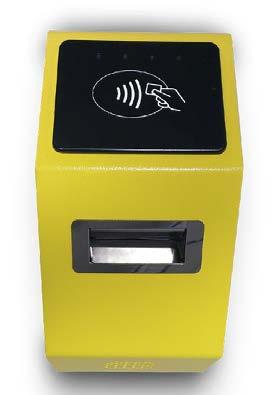
9 Cluster specialization Devices & apparatus Solar modules Electric energy meter Medical equipment Telecom apparatus Energy-efficient appliances Radiation control Security systems POS terminals Transport Validator

10 Cluster specialization Equipment Microelectronics control Microscopes (ATM) Nanotube production Thermal processing Epitaxial equipment Laser equipment for microand nano-processing


11 Projects cluster development Examples of projects The creation of a centre for advanced access to the latest core technologies for 3D integration of products of micro - and nanoelectronics and electronic devices based on them The creation of a specialized diagnostic-metrological centre shared services research, diagnosis, measurement and testing parts warehouse, including in the nanometer range Design Center of modern microelectronic components in remote access to centralized computing resources 11
12 Thank you for attention See you in Zelenograd
Innovative cluster Zelenograd
 Innovative cluster Zelenograd Location Innovative technology cluster Zelenograd (Moscow, Zelenograd) Zelenograd background: Total area 3720 hectares Population 229 600 Industrial personnel 23 000 60% of
The role of the technology platform «Medicine of the Future» in biomedical innovations development. Kurzina Irina 21 May 2014, Moscow
 The role of the technology platform «Medicine of the Future» in biomedical innovations development Kurzina Irina 21 May 2014, Moscow Organizational Structure The strategic target of the Technology platform
Technology transfer and business development for innovation projects. From local market to global industry.
 Technology transfer and business development for innovation projects. From local market to global industry. www.zntc.ru Well positioned for innovative business development Fab и Lab R&D Multifunctional
Course Outcome of M.Tech (VLSI Design)
") Course Outcome of M.Tech (VLSI Design) PVL108: Device Physics and Technology The students are able to: 1. Understand the basic physics of semiconductor devices and the basics theory of PN junction. 2.
Course Outcome of M.Tech (VLSI Design) PVL108: Device Physics and Technology The students are able to: 1. Understand the basic physics of semiconductor devices and the basics theory of PN junction. 2.
DSP Valley Designing Smart Products
 DSP Valley Designing Smart Products Engineering Mobility Days Coimbra 21-5-2014 Slide 1 Outline 1. DSP Valley? 2. Jobopportunities within the network General information Jobs and company profiles 3. Application
JSC Progress MRI. ACTIVITY AREAS, EXPERIENCE and SUGGESTIONS
 JSC Progress MRI ACTIVITY AREAS, EXPERIENCE and SUGGESTIONS JSC Progress Microelectronic Research Institute is - Leading design centre of the Russian Federation on the development of specialized microelectronic
Model of Open Innovation IMEC IIAP: a View from Russia
 "Again I say to you, that if two of you agree on Earth about anything that they may ask, it shall be done for them by My Father who is in Heaven. Holy Bible, Matthew 18:19 It seems like for the time being
Kaben Wireless Silicon and Triad Semiconductor Partnership. Wireless & RF ASICs for Everyone!
 Kaben Wireless Silicon and Triad Semiconductor Partnership Wireless & RF ASICs for Everyone! Kaben Wireless Silicon & Triad Semiconductor Pursue a Comprehensive Partnership Triad Semiconductor Via Configurable
Georgia Electronic Commerce Association. Dr. G. Wayne Clough, President Georgia Institute of Technology April 30, 2003
 Georgia Electronic Commerce Association Dr. G. Wayne Clough, President Georgia Institute of Technology April 30, 2003 Georgia Tech: Driving high-end economic development Oak Ridge National Laboratory National
CMOS VLSI IC Design. A decent understanding of all tasks required to design and fabricate a chip takes years of experience
 CMOS VLSI IC Design A decent understanding of all tasks required to design and fabricate a chip takes years of experience 1 Commonly used keywords INTEGRATED CIRCUIT (IC) many transistors on one chip VERY
Specialization in Microelectronics. Wang Qijie Nanyang Assistant Professor in EEE March 8, 2013
 Specialization in Microelectronics Wang Qijie Nanyang Assistant Professor in EEE qjwang@ntu.edu.sg March 8, 2013 Electronic Engineering Option Microelectronics What is it about? Study of semiconductor
Core Business: Semiconductor-related Inspection Equipment
 Core Business: Semiconductor-related Inspection Equipment Lasertec manufactures unique inspection and measurement systems that incorporate the cutting-edge technologies of applied optics and offers them
A European Perspective for Electronic Industry in Latin America
 A European Perspective for Electronic Industry in Latin America François Guibert Corporate Vice President, Emerging Markets Region General Manager Electronic, a Global World Security Networking Consumer
End-of-line Standard Substrates For the Characterization of organic
 FRAUNHOFER INSTITUTe FoR Photonic Microsystems IPMS End-of-line Standard Substrates For the Characterization of organic semiconductor Materials Over the last few years, organic electronics have become
Recent Developments in Multifunctional Integration. Stephan Guttowski, Head of Technology Park»Heterointegration«, Fraunhofer FMD
 Recent Developments in Multifunctional Integration Stephan Guttowski, Head of Technology Park»Heterointegration«, Fraunhofer FMD Founding Participants 2 One-Stop-Shop for developments from wafer technologies
Compound Semiconductor Center
 Compound Semiconductor Center Compound Semiconductor Centre Building a Technology Cluster in South Wales Dr Wyn Meredith Status October 2015 Formal JV: 50:50 Cardiff University: IQE Academia Public Sector
Stakeholder engagement
 Stakeholder engagement Dr Malcolm Parry OBE, Managing Director and CEO The Surrey Research Park, University of Surrey Stakeholders objectives - host University / other hosts Some independent income Raise
Index. Cambridge University Press Silicon Photonics Design Lukas Chrostowski and Michael Hochberg. Index.
 absorption, 69 active tuning, 234 alignment, 394 396 apodization, 164 applications, 7 automated optical probe station, 389 397 avalanche detector, 268 back reflection, 164 band structures, 30 bandwidth
During the blur of activity of the coming months, we look forward to meeting and collaborating with many of you.
 Newsletter N 3, September 2011. Giles BRANDON Alexander KOROTKOV Johann Hauer (Intelligentsia Consultants Ltd) (St Petersburg State Polytechnical University) (Fraunhofer IIS) Project coordinator Russian
FRAUNHOFER INSTITUTE FOR PHOTONIC MICROSYSTEMS IPMS. Application Area. Quality of Life
 FRAUNHOFER INSTITUTE FOR PHOTONIC MICROSYSTEMS IPMS Application Area Quality of Life Overlay image of visible spectral range (VIS) and thermal infrared range (LWIR). Quality of Life With extensive experience
EE 434 Lecture 2. Basic Concepts
 EE 434 Lecture 2 Basic Concepts Review from Last Time Semiconductor Industry is One of the Largest Sectors in the World Economy and Growing All Initiatives Driven by Economic Opportunities and Limitations
BIOMEDICAL ELECTRONICS. Date & Day II - SEMESTER ADVANCED MEDICAL IMAGING DIAGNOSTIC AND THERAPEUTIC EQUIPMENT MEDICAL PRODUCT DESIGN
 OSMANIA UNIVERSITY, HYDERABAD - 7 M. E. (BME) (Main) Examination, September 2013 EXAMINATION TIME TABLE Time : 2.00 PM to 5.00 PM Department of BME Date & Day BIOMEDICAL ELECTRONICS II - SEMESTER ADVANCED
2010 IRI Annual Meeting R&D in Transition
 2010 IRI Annual Meeting R&D in Transition U.S. Semiconductor R&D in Transition Dr. Peter J. Zdebel Senior VP and CTO ON Semiconductor May 4, 2010 Some Semiconductor Industry Facts Founded in the U.S. approximately
Energy & Space. International Presentations
 Energy & Space International Presentations 2012-2013 Advanced Electronics 3D Printed Circuit Boards 3D Printed Circuit Boards for Solder-Free Printable Electronics 4x4 Vehicles Arduino WiFi Android Controllers
Visvesvaraya Technological University, Belagavi
 Time Table for M.TECH. Examinations, June / July 2017 M. TECH. 2010 Scheme 2011 Scheme 2012 Scheme 2014 Scheme 2016 Scheme [CBCS] Semester I II III I II III I II III I II IV I II Time Date, Day 14/06/2017,
Internet of Things. (Ref: Slideshare)
") Internet of Things (Ref: Slideshare) Contents Introduction/Overview The Internet of Things Applications of IoT Challenges and Barriers in IoT Future of IoT Internet Revolution Impact of the Internet Education
Internet of Things (Ref: Slideshare) Contents Introduction/Overview The Internet of Things Applications of IoT Challenges and Barriers in IoT Future of IoT Internet Revolution Impact of the Internet Education
EPD ENGINEERING PRODUCT DEVELOPMENT
 EPD PRODUCT DEVELOPMENT PILLAR OVERVIEW The following chart illustrates the EPD curriculum structure. It depicts the typical sequence of subjects. Each major row indicates a calendar year with columns
The SEMATECH Model: Potential Applications to PV
 Continually cited as the model for a successful industry/government consortium Accelerating the next technology revolution The SEMATECH Model: Potential Applications to PV Dr. Michael R. Polcari President
DTMOS IV Efficiency Advantages of Superjunction Transistors. By Michael Piela, Toshiba Electronics Europe
 DTMOS IV Efficiency Advantages of Superjunction Transistors By Michael Piela, Toshiba Electronics Europe Summary Superjunction MOSFETs are able to deliver a combination of high conduction and switching
BS in. Electrical Engineering
 BS in Electrical Engineering Program Objectives Habib University s Electrical Engineering program is designed to impart rigorous technical knowledge, combined with hands-on experiential learning and a
Development of infrastructure for 3D TSV packaging technology at the facilities of Zelenograd Nanotechnology Center
 Development of infrastructure for 3D TSV packaging technology at the facilities of Zelenograd Nanotechnology Center SEMICON Russia, June 6, 2013 Session II: 3D Packaging and TSV Project in Russia: Overview
One-Stop-Shop for. Research Fab Microelectronics Germany
 Fraunhofer Group for Microelectronics One-Stop-Shop for Technologies and Systems Research Fab Microelectronics Germany The entire added-value chain for microelectronics and nanoelectronics from a single
Des MEMS aux NEMS : évolution des technologies et des concepts aux travers des développements menés au LETI
 Des MEMS aux NEMS : évolution des technologies et des concepts aux travers des développements menés au LETI Ph. Robert 1 Content LETI at a glance From MEMS to NEMS: 30 years of technological evolution
Carinthia continues to expand Villach as a microelectronics research cluster
 Pressemitteilung CTR Carinthian Tech Research AG Mag Birgit Rader-Brunner 01.02.2017 http://idw-online.de/de/news667249 Forschungs- / Wissenstransfer, Wissenschaftspolitik Chemie, Elektrotechnik, Physik
Canada s National Design Network. Community Research Innovation Opportunity
 Canada s National Design Network Community Research Innovation Opportunity Over the past five years, more than 7000 researchers in the National Design Network have benefited from industrial tools, technologies,
The role of university science parks in business-university research collaboration
 The role of university science parks in business-university research collaboration The Dowling Review: enhancing business-university research collaboration Dr Malcolm Parry OBE, Director and CEO The Surrey
MEDIA RELEASE FOR IMMEDIATE RELEASE 26 JULY 2016
 MEDIA RELEASE FOR IMMEDIATE RELEASE 26 JULY 2016 A*STAR S IME KICKS OFF CONSORTIA TO DEVELOP ADVANCED PACKAGING SOLUTIONS FOR NEXT-GENERATION INTERNET OF THINGS APPLICATIONS AND HIGH-PERFORMANCE WIRELESS
Triple i - The key to your success
 Triple i - The key to your success The needs and challenges of today s world are becoming ever more demanding. Standards are constantly rising. Creativity, reliability and high performance are basic prerequisites
Formal Hardware Verification: Theory Meets Practice
 Formal Hardware Verification: Theory Meets Practice Dr. Carl Seger Senior Principal Engineer Tools, Flows and Method Group Server Division Intel Corp. June 24, 2015 1 Quiz 1 Small Numbers Order the following
DARPA TRUST in IC s Effort. Dr. Dean Collins Deputy Director, MTO 7 March 2007
 DARPA TRUST in IC s Effort Dr. Dean Collins Deputy Director, MTO 7 March 27 Report Documentation Page Form Approved OMB No. 74-88 Public reporting burden for the collection of information is estimated
IBM Research - Zurich Research Laboratory
 October 28, 2010 IBM Research - Zurich Research Laboratory Walter Riess Science & Technology Department IBM Research - Zurich wri@zurich.ibm.com Outline IBM Research IBM Research Zurich Science & Technology
Ankit A. Shukla Practise Director, Technical Insights
 Russian Microelectronics Market: Current State and Development Opportunities November 1, 2013 Ankit A. Shukla Practise Director, Technical Insights Global Microelectronics Market Total market size USD
EE 434 ASIC and Digital Systems. Prof. Dae Hyun Kim School of Electrical Engineering and Computer Science Washington State University.
 EE 434 ASIC and Digital Systems Prof. Dae Hyun Kim School of Electrical Engineering and Computer Science Washington State University Preliminaries VLSI Design System Specification Functional Design RTL
300mm BEOL manufacturing capabili=es in Russia. November 2017 CNE PROPRIETARY
 300mm BEOL manufacturing capabili=es in Russia November 2017 About CNE CNE is a pure-play 300mm BEOL Foundry with state of the art equipment, advanced process technologies and capabiliees Crocus Nano Electronics
Moving from Nano-Ideas to Nanomanufacturing. Alan Rae February 2008
 Moving from Nano-Ideas to Nanomanufacturing Alan Rae February 2008 Topics What s different in nanomanufacturing? Technology development and acquisition Commercialization issues Some examples of products
INTERNATIONAL ELECTRONIC CONFERENCE ON SENSORS AND APPLICATIONS
 INTERNATIONAL ELECTRONIC CONFERENCE ON SENSORS AND APPLICATIONS 01 16 JUNE 2014 AUTHORS / RESEARCHERS A.F.M. Anuar, Y. Wahab, H. Fazmir, M. Najmi, S. Johari, M. Mazalan, N.I.M. Nor, M.K. Md Arshad Advanced
Innovative Technology for Innovative Science Hands-on in a Nanoscience Classroom
 Innovative Technology for Innovative Science Hands-on in a Nanoscience Classroom Presented by Jennifer F. Wall, Ph.D. Imaging Possibilities Optical 2 mm Electron 500 microns Atomic Force 10 microns Scanning
Are innovative sensor concepts included in the funding programmes of the EU and Germany? Dr. Bernhard Ruf, VDI/VDE-IT
 Are innovative sensor concepts included in the funding programmes of the EU and Germany? Dr. Bernhard Ruf, VDI/VDE-IT VDI/VDE IT: Who we are? Company Employees: ca. 270 Turnover (2012): 24,8 Mio. Share
SEMICONDUCTOR INDUSTRY ASSOCIATION FACTBOOK
 Factbook 2014 SEMICONDUCTOR INDUSTRY ASSOCIATION FACTBOOK INTRODUCTION The data included in the 2014 SIA Factbook helps demonstrate the strength and promise of the U.S. semiconductor industry and why it
POSSUM TM Die Design as a Low Cost 3D Packaging Alternative
 POSSUM TM Die Design as a Low Cost 3D Packaging Alternative The trend toward 3D system integration in a small form factor has accelerated even more with the introduction of smartphones and tablets. Integration
STM RH-ASIC capability
 STM RH-ASIC capability JAXA 24 th MicroElectronic Workshop 13 th 14 th October 2011 Prepared by STM Crolles and AeroSpace Unit Deep Sub Micron (DSM) is strategic for Europe Strategic importance of European
Consortium Capabilities
 Consortium Capabilities The driver in advanced materials development is to create products with competitive advantages. Products must continuously become faster, lighter and cheaper and must provide additional
2020 at the Horizon. Upcoming calls in Electronics. "Competitive Electronics Industry" "Digital Industry" "CONNECT"
 2020 at the Horizon Upcoming calls in Electronics Andreas Lymberis-Henri Rajbenbach Unit A3: Directorate: Directorate General: "Competitive Electronics Industry" "Digital Industry" "CONNECT" Electronic
nanovea.com PROFILOMETERS 3D Non Contact Metrology
 PROFILOMETERS 3D Non Contact Metrology nanovea.com PROFILOMETER INTRO Nanovea 3D Non-Contact Profilometers are designed with leading edge optical pens using superior white light axial chromatism. Nano
1 Introduction 1.1 HISTORICAL DEVELOPMENT OF MICROELECTRONICS
 1 Introduction 1.1 HISTORICAL DEVELOPMENT OF MICROELECTRONICS The field of microelectronics began in 1948 when the first transistor was invented. This first transistor was a point-contact transistor, which
Design of MEMS Piezoelectric Vibrational Energy Harvesters for Industrial and Commercial Applications
 Design of MEMS Piezoelectric Vibrational Energy Harvesters for Industrial and Commercial Applications Consumer Applications Civil Infrastructure Kathleen M. Vaeth, Vice President of Engineering microgen
PERSPECTIVES FOR DISRUPTIVE 200MM/8-INCH GAN POWER DEVICE AND GAN-IC TECHNOLOGY DR. DENIS MARCON SR. BUSINESS DEVELOPMENT MANAGER
 PERSPECTIVES FOR DISRUPTIVE 200MM/8-INCH GAN POWER DEVICE AND GAN-IC TECHNOLOGY DR. DENIS MARCON SR. BUSINESS DEVELOPMENT MANAGER What I will show you today 200mm/8-inch GaN-on-Si e-mode/normally-off technology
EPD ENGINEERING PRODUCT DEVELOPMENT
 EPD PRODUCT DEVELOPMENT PILLAR OVERVIEW The following chart illustrates the EPD curriculum structure. It depicts the typical sequence of subjects. Each major row indicates a calendar year with columns
Digital innovation competences = apprx. 1/3 of income TRL 1-8 specific focus TRL 4+
 (since 1949) The largest Slovenian scientific research institute in this part of Europe 1000 employes, 420 ongoing international projects Slovenia on EU KET and DIH map Key Enabling Technologies Technology
Selected Topics in Nanoelectronics. Danny Porath 2002
 Selected Topics in Nanoelectronics Danny Porath 2002 Links to NST http://www.foresight.org/ http://itri.loyola.edu/nanobase/ http://www.zyvex.com/nano/ http://www.nano.gov/ http://www.aeiveos.com/nanotech/
Studying at preparing courses Studying at PC (Russian language 10 months) Study at PC (Russian language, entrance after 1-st of
 Study at PC (Russian language, entrance after 1-st of") Cost for foreign students at the Faculty of International Education NTU "KhPI" in 2016/2017 academic year to students enrolled on an individual contract Type of study Cost per 1 year, in $ Studying at
Cost for foreign students at the Faculty of International Education NTU "KhPI" in 2016/2017 academic year to students enrolled on an individual contract Type of study Cost per 1 year, in $ Studying at
DTU DANCHIP an open access micro/nanofabrication facility bridging academic research and small scale production
 DTU DANCHIP an open access micro/nanofabrication facility bridging academic research and small scale production DTU Danchip National Center for Micro- and Nanofabrication DTU Danchip DTU Danchip is Denmark
IHP Innovations for High Performance Microelectronics
 IHP Innovations for High Performance Microelectronics IHP - Innovations for High Performance Microelectronics in Frankfurt (Oder) is known for internationally acknowledged research at the highest level.
Innovative antimicrobial additive for building finishing materials
 Technology Offer Innovative antimicrobial additive for building finishing materials Summary A university spin-off from Latvia has developed an innovative, environmentally friendly type of antimicrobial
RESPONSIBILITY OF THE SEMICONDUCTOR DESIGN INFRASTRUCTURE
 RESPONSIBILITY OF THE SEMICONDUCTOR DESIGN INFRASTRUCTURE C O N S U L T I N G I N E L E C T R O N I C D E S I G N Lucio Lanza gave a keynote at IC CAD 2010 that caught a lot of people s attention. In that
Business Opportunity. The wave is coming. The Opportunity. Time Synchronization as a first-order concept You take care of it, or you will pay for it!
 Business Opportunity. The wave is coming. The Opportunity Time Synchronization as a first-order concept You take care of it, or you will pay for it! www.sevensols.com Seven Solutions - When every nanosecond
National Projects on Semiconductor in NEDO
 National Projects on Semiconductor in NEDO June 17, 2011 Toru Nakayama New Energy and Industrial Technology Development Organization (NEDO), Japan Contents About NEDO NEDO s projects for semiconductor
Stream Profiles Career Opportunities
 Stream Profiles Career Opportunities As a Industrial & Control Engineer, You can be Control engineer, Modeling engineer, Development engineer, Test and validation engineer, Robotics Engineer R&D Electrical
My USM. Mustafa G. Guvench. Professor, Electrical Engineering
 My Projects @ USM Mustafa G. Guvench Professor, Electrical Engineering My Interests & Expertise CMOS Analog I.C. Design Silicon I.C. Processing Micro Machining and MEMS Optoelectronics (Photosensors( Photosensors)
Computer Aided Design of Electronics
 Computer Aided Design of Electronics [Datorstödd Elektronikkonstruktion] Zebo Peng, Petru Eles, and Nima Aghaee Embedded Systems Laboratory IDA, Linköping University www.ida.liu.se/~tdts01 Electronic Systems
Nanotechnology, the infrastructure, and IBM s research projects
 Nanotechnology, the infrastructure, and IBM s research projects Dr. Paul Seidler Coordinator Nanotechnology Center, IBM Research - Zurich Nanotechnology is the understanding and control of matter at dimensions
KEY ENABLING TECHNOLOGIES
 KEY ENABLING TECHNOLOGIES AND SMART SPECIALISATION FOR A COMPETITIVE ITALY PROF. GABRIEL M CREAN VICE-PRESIDENT FOR TECHNOLOGY, CEA, FRANCE, HIGH LEVEL GROUP ON KEY ENABLING TECHNOLOGIES Bari, 23th of
research in the fields of nanoelectronics
 FRAUNHOFEr center Nanoelectronic Technologies research in the fields of nanoelectronics 1 contents Fraunhofer CNT in Profile 3 Competence Areas Analytics 4 Functional Electronic Materials 5 Device & Integration
EU-Russia Meeting on R&D Collaboration Moscow, 25 September 2007
 EU-Russia Meeting on R&D Collaboration Moscow, 25 September 2007 The FP7 ICT Theme Components & Systems Dr Erastos Filos European Commission Information Society and Media Directorate-General EF_Comp+Syst_FP7ICT_25Sep07-1
Developing Smart Miniaturized Solutions for Industry
 Developing Smart Miniaturized Solutions for Industry Micro nanotechnologies & Embedded Software Competitive Cluster - Grenoble / France www.minalogic.com Born in Grenoble 1 st french scanner (1972) Airbag
4+0_100A3_170g.job Sig:1-A Composite
 4+0_100A3_170g.job Sig:1-A Composite Introduction We would like to welcome you to the SEMIDEC Promotion Guide of Russian Semiconductor Design. Russia has a proud heritage in semiconductor components dating
Putting PICs in Products A Practical Guideline. Katarzyna Ławniczuk
 Putting PICs in Products A Practical Guideline Katarzyna Ławniczuk k.lawniczuk@brightphotonics.eu Outline Product development considerations Selecting PIC technology Design flow and design tooling considerations
Semiconductor Process Diagnosis and Prognosis for DSfM
 Semiconductor Process Diagnosis and Prognosis for DSfM Department of Electronic Engineering Prof. Sang Jeen Hong Nov. 19, 2014 1/2 Agenda 1. Semiconductor Manufacturing Industry 2. Roles of Semiconductor
Rick Clemmer Media briefing in China. Rick Clemmer, President & CEO NXP Semiconductors March 19, 2012 Shanghai
 Rick Clemmer Media briefing in China Rick Clemmer, President & CEO NXP Semiconductors March 19, 2012 Shanghai Today s agenda NXP update Share our vision Zoom in China 2 NXP Semiconductors NXP Semiconductors
Highly Sensitive Filter-Less Fluorescence Detection Method Using an Avalanche Photodiode
 Journal of Energy and Power Engineering 10 (2016) 268-273 doi: 10.17265/1934-8975/2016.04.008 D DAVID PUBLISHING Highly Sensitive Filter-Less Fluorescence Detection Method Using an Avalanche Photodiode
EU's contribution to research and innovation in Electronics
 EU's contribution to research and innovation in Electronics Henri.RAJBENBACH@ec.europa.eu Nikolaos.KYRLOGLOU@ec.europa.eu European Commission DG CONNECT (not legally binding presentation) SEMICON Europa-Flex
Photolithography I ( Part 1 )
") 1 Photolithography I ( Part 1 ) Chapter 13 : Semiconductor Manufacturing Technology by M. Quirk & J. Serda Bjørn-Ove Fimland, Department of Electronics and Telecommunication, Norwegian University of Science
1 Photolithography I ( Part 1 ) Chapter 13 : Semiconductor Manufacturing Technology by M. Quirk & J. Serda Bjørn-Ove Fimland, Department of Electronics and Telecommunication, Norwegian University of Science
BRIEF OVERVIEW OF THE CERTI SYSTEM
 BRIEF OVERVIEW OF THE CERTI SYSTEM 1 Profile and Aim Nature: Private, non-profit, RD&I institution. Size: ~ 350 employees Mission: To provide strategic and innovative solutions to our customers, based
FRAUNHOFER GROUP FOR MICROELECTRONICS ONE-STOP-SHOP FOR TECHNOLOGIES AND SYSTEMS
 FRAUNHOFER GROUP FOR MICROELECTRONICS ONE-STOP-SHOP FOR TECHNOLOGIES AND SYSTEMS The entire added-value chain for microelectronics and nanoelectronics from a single provider The Research Fab Microelectronics
Dassault Systèmes in High-Tech
 Dassault Systèmes in High-Tech London September 3 rd, 2014 Olivier RIBET Vice-President, High Tech Industry 1 High-Tech: Driver of Innovation across Industries Connect Product, Nature & Life is the challenge
Cutting-edge Atomic Force Microscopy techniques for large and multiple samples
 Cutting-edge Atomic Force Microscopy techniques for large and multiple samples Study of up to 200 mm samples using the widest set of AFM modes Industrial standards of automation A unique combination of
Competitive cluster Micro-Nano Technologies and Embedded Software Grenoble - Isère / France
 Competitive cluster Micro-Nano Technologies and Embedded Software Grenoble - Isère / France What is a Competitive Cluster? Within a well defined geographical area, a cluster gathers - industries, - research
RealNano & ACINTECH Projektbeispiele für Nanotechnologie in der Mikroelektronik
 RealNano & ACINTECH Projektbeispiele für Nanotechnologie in der Mikroelektronik Reinhold Ebner, Anton Köck, Stefan Defregger Materials Center Leoben Forschung GmbH Roseggerstrasse 12 A-8700 Leoben www.mcl.at
Promotion guide of Russian Semiconductor Design Organisations
 Promotion guide of Russian Semiconductor Design Organisations INTRODUCTION This is a promotion guide of Russian R&D organisations and companies eager to develop international cooperation in semiconductor
Quantum Design Japan. Introducing Advanced Technology to Japan
 Introducing Advanced Technology to Japan Profile Incorp. date: July 1, 1997 Ownership: Business: Offices: Employees: Revenue: < $25M Address: Subsidiary of Quantum Design www.qdusa.com Sales and service
In 1984, a cell phone in the U.S. cost $3,995 and
 In 1984, a cell phone in the U.S. cost $3,995 and weighed 2 pounds. Today s 8GB smartphones cost $199 and weigh as little as 4.6 oz. Technology Commercialization Applied Materials is one of the most important
MAPPER: High throughput Maskless Lithography
 MAPPER: High throughput Maskless Lithography Marco Wieland CEA- Leti Alterative Lithography workshop 1 Today s agenda Introduction Applications Qualification of on-tool metrology by in-resist metrology
Laboratorio de Innovación en MEMS (LI-MEMS) Ceremonia de Inauguración Tonantzintla, Pue., de abril de 2010 Auditorio del Centro de Información
 Ceremonia de Inauguración Tonantzintla, Pue., de abril de 2010 Auditorio del Centro de Información") Instituto Nacional de Astrofísica, Óptica y Electrónica Laboratorio de Innovación en MEMS (LI-MEMS) Ceremonia de Inauguración Tonantzintla, Pue., 19-20 de abril de 2010 Auditorio del Centro de Información
Instituto Nacional de Astrofísica, Óptica y Electrónica Laboratorio de Innovación en MEMS (LI-MEMS) Ceremonia de Inauguración Tonantzintla, Pue., 19-20 de abril de 2010 Auditorio del Centro de Información
Noel Technologies. Provider of Advanced Lithography and Semiconductor Thin Film Services
 Noel Technologies Provider of Advanced Lithography and Semiconductor Thin Film Services Noel Technologies Keith Best Biography Over the last 27 years, Keith Best has held a variety of semiconductor processing
PLAN OF SECOND DEGREE POSTGRADUATE STUDY
 Zał. nr 1 do uchwały nr 44/2015 Rady Wydziału Elektrycznego PB z dnia 20.05.2015 r. BIALYSTOK UNIVERSITY OF TECHNOLOGY FACULTY OF ELECTRICAL ENGINEERING PLAN OF SECOND DEGREE POSTGRADUATE STUDY course
Beyond Moore the challenge for Europe
 Beyond Moore the challenge for Europe Dr. Alfred J. van Roosmalen Vice-President Business Development, NXP Semiconductors Company member of MEDEA+/CATRENE/AENEAS/Point-One FIT-IT 08 Spring Research Wien,
RUSNANO 10A Prospekt 60-letiya Oktyabrya, Moscow, , Russia P: F: E:
 RUSNANO 10A Prospekt 60-letiya Oktyabrya, Moscow, 117036, Russia P: +7 495 988 5388 F: +7 495 988 5399 E: info@rusnano.com www.rusnano.com FOSTERING A NEW INDUSTRY ELECTRONICS HEALTH METALLURGY & INSTRUMENT
AN INVISIBLE TRACKNIG SYSTEM DURING NATURAL CALAMITIES
 AN INVISIBLE TRACKNIG SYSTEM DURING NATURAL CALAMITIES L. RAMU NAIK 1, MR.ASHOK 2 1 L. Ramu Naik, M.Tech Student, Aryabhata Institute Of Technology & Science, Maheshwaram X Roads, On Srisailam Highway,
EMERGING INKJET PRINTING TECHNOLOGIES, APPLICATIONS AND GLOBAL MARKETS
 EMERGING INKJET PRINTING TECHNOLOGIES, APPLICATIONS AND GLOBAL MARKETS AVM091B November 2014 Andrew McWilliams Project Analyst ISBN: 1-56965-999-0 BCC Research 49 Walnut Park, Building 2 Wellesley, MA
THIS IS INNOVATION Compound Semiconductors
 THIS IS INNOVATION Compound Semiconductors E N A B L I N G This is a quiet industrial revolution, nudging forward the capabilities of the electronics which hide inside nearly every modern day device and