Parallel Alignment of Nanowires for Fast Fabrication of Nanowire Based Gas Sensors
|
|
|
- Melinda Quinn
- 5 years ago
- Views:
Transcription

1 Parallel Alignment of Nanowires for Fast Fabrication of Nanowire Based Gas Sensors R. Jiménez-Díaz 1, J.D. Prades 1 F. Hernández-Ramírez, J. Santander 3 C. Calaza 3, L. Fonseca 3, C. Cané 3 A. Romano-Rodriguez 1 1 MIND-IN UB, Dept. Electrònica, Universitat de Barcelona, Spain IREC, Barcelona, Spain 3 Instituto de Microelectrónica de Barcelona, IMB-CNM-CSIC, Bellaterra, Spain Previous work Nanowires offer attractive features to improve many of the issues in solid state gas sensors
 Previous work Stability Nanotechnol. 18, 49551 (7) Sens.")
2 Previous work Sensitivity Adv. Funct. Mater. 18, 99 (8) Previous work Stability Nanotechnol. 18, (7) Sens.Actuatators B 144, 1 (1)
 1 1 [NO ] (ppm).1 1 1.1 15 3 45 6 75 9 15 1 135 time (minutes) Sens. Actuators B 14, 337 (9) PCCP, in press (1)")
3 Previous work Response time PCCP 11, 715 (9) Previous work Working temperature response S(%) UV - OFF (T=5ºC) UV - ON (T=5ºC) 1 1 [NO ] (ppm) time (minutes) Sens. Actuators B 14, 337 (9) PCCP, in press (1)


4 Previous work Power consumption very low power consumption: less than μw (measurement AND HEATING included!!!) APL 93, 1311 (8) APL 95, 5311 (9) Previous work Nanowires offer attractive features to improve many of the issues in solid state gas sensors Sensitivity radius response Stability pristine surface fully reversible response Response time indiv. nanowire no gas diffusion Working temperature UV light room temperature operation Power consumption indiv. nanowire self-heating effect ultra-low power consumption fully autonomous gas sensors faster devices Challenge: dealing with nanofabrication issues


5 Contacting & Measuring One Single Nanowire Dual-beam Focused-Ion Beam Ion-assisted deposited platinum stripe among 4 gold microelectrodes Deposit Pt-containing material (from PtC 9 H 16 ) Auger Electron Spectr.: C (67%) + Pt (7%) With ions or with electrons ρ ions = 1 ρ Pt-metal ρ electrons = 1 5 ρ Pt-metal 1 1 A/m Thermally stable up to 65 K Contacting & Measuring One Single Nanowire Nanowires are dispersed over a substrate with pre-patterned patterned μelectrodes SnO Nanowires Nanotechnology 17, (6)

 - Platinum contacts - Reproducible")
 Metal oxide NW Mostly")
 6 3-3 Self-heating at")
 Physical Review B 76, 8549 (7)")
6 Contacting & Measuring One Single Nanowire Nanolithography Process - Sequential e-beam e & i-beam i depositions L = 11 μm r 5 nm Nanotechnology 17, (6) - Platinum contacts - Reproducible process - Can be used on demand Contacting & Measuring One Single Nanowire Electrical Characterization (- & 4-probes) Metal oxide NW Mostly non-ohmic responses High contact resistances Study of the NW requires 4p Current (na) Self-heating at contacts Voltage (V) Nanotechnology 17, (6) Physical Review B 76, 8549 (7)


 + ( σ σ σ ) m p m ε m ω + σ m p m")
 4x1 5 3x1 5 x1 5 1x1 5 Re{K} Experimental")
 Design of electrodes Based")

7 Dielectrophoretic alignment of NWs Self-assembly technique When a polarizable NW is subject to a non-uniform electric field a dipole moment is induced that tends to align the nanowire in the direction of the electric field Proof of concept experiments Dielectrophoretical force when applying an electrical field in a dielectric medium: 1 FDEP = π r l ε m Re{ K} E RMS 6x1 5 ω Re{ K} = ( ε ε ε ) + ( σ σ σ ) m p m ε m ω + σ m p m m 5x1 5 4 Re{K} (a.u.) 4x1 5 3x1 5 x1 5 1x1 5 Re{K} Experimental results Alignment Yield (a.u.) Frequency (Hz) Dielectrophoretic alignment of NWs Design of electrodes Based on big electrodes with sharp tips opposed. Gaps of different lengths Au SiO Au Au SiO SiO Au Au SiO SiO

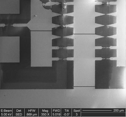


8 Dielectrophoretic alignment of NWs Results on alignment of nanowires: Dielectrophoretic alignment of NWs Big difference! BEFORE NOW!
. Phys.Rev.")
 -1 ρ DEP =.38 ±.")

9 Dielectrophoretic alignment of NWs -probes configuration rectifying behavior Schottky diodes (NW // Pt FIB). Phys.Rev.B 76, 8549 (7) 4-probes configuration SnO -NW ρ EIB =.4 ±. (Ωcm) -1 ρ DEP =.38 ±. (Ωcm) -1 Gas Sensor Measurements Carbon monoxide Aligned SnO -NW Diameter: 9nm R CO /R SA 1,,8,6,4, R CO /R SA at T = 375 K R CO /R SA at T = 45 K CO concentration, time (hours) [CO] (ppm)
10 Gas Sensor Measurements Comparison with non-dep experiments: Adv. Funct. Mater. 18, 99 (8) Conclusions Individual NWs can be electrically contacted with the help of FIB lithography techniques Gas nanosensors can be fabricated using these techniques, responding to different gases (SA, N, CO, H O) Alignment of nanowires by dielectrophoretic feasible techniques is Gas nanosensors with equivalent properties as non-dep aligned NWs can be fabricated This allows the increase of the throughput in gas sensor fabrication based on individual NWs
11 Acknowledgments This work was partially supported by: European Union through projects NANOS4 and ARI (Access to Research Infrastructures) Spanish Ministry of Science and Technology, through the projects MAGASENS, CROMINA and NAWACS (NanoSciERA programme) and FPU grants. This work has been developed partially using the capacities of ICTS Clean room of micro & nano fabrication of IMB-CNM (CSIC). Thank you all for your attention!
Low-Power Heating for Conductometric Gas Nano Sensors: Self-Heating Effects and Others
 TITLE Low-Power Heating for Conductometric Gas Nano Sensors: Self-Heating Effects and Others SPEAKER O. Monereo, N. Markiewicz, J. Samà, O. Casals, C. Fàbrega, F. Hernandez-Ramírez, A. Cirera, A. Romano-Rodríguez,
Available online at ScienceDirect. Procedia Engineering 168 (2016 ) th Eurosensors Conference, EUROSENSORS 2016
 th Eurosensors Conference, EUROSENSORS 2016") Available online at www.sciencedirect.com ScienceDirect Procedia Engineering 168 (2016 ) 1056 1060 30th Eurosensors Conference, EUROSENSORS 2016 Site-selectively grown p-type Ge NWs as a gas sensor J.
Available online at www.sciencedirect.com ScienceDirect Procedia Engineering 168 (2016 ) 1056 1060 30th Eurosensors Conference, EUROSENSORS 2016 Site-selectively grown p-type Ge NWs as a gas sensor J.
Recent Technological Developments on LGAD and ilgad Detectors for Tracking and Timing Applications
 Recent Technological Developments on LGAD and ilgad Detectors for Tracking and Timing Applications G. Pellegrini 1, M. Baselga 1, M. Carulla 1, V. Fadeyev 2, P. Fernández-Martínez 1, M. Fernández García
Nanostencil Lithography and Nanoelectronic Applications
 Microsystems Laboratory Nanostencil Lithography and Nanoelectronic Applications Oscar Vazquez, Marc van den Boogaart, Dr. Lianne Doeswijk, Prof. Juergen Brugger, LMIS1 Dr. Chan Woo Park, Visiting Professor
Bottom-up Nanostructures just a research hype?
 Fakultät Maschinenwesen, Institut für Werkstoffwissenschaft, Professur Materialwissenschaft u. Nanotechnik Bottom-up Nanostructures just a research hype? Dr.-Ing. Alexander Nerowski Dresden, 22.09.2017
The HGTD: A SOI Power Diode for Timing Detection Applications
 The HGTD: A SOI Power Diode for Timing Detection Applications Work done in the framework of RD50 Collaboration (CERN) M. Carulla, D. Flores, S. Hidalgo, D. Quirion, G. Pellegrini IMB-CNM (CSIC), Spain
Electrical transport properties in self-assembled erbium. disilicide nanowires
 Solid State Phenomena Online: 2007-03-15 ISSN: 1662-9779, Vols. 121-123, pp 413-416 doi:10.4028/www.scientific.net/ssp.121-123.413 2007 Trans Tech Publications, Switzerland Electrical transport properties
A 30 GHz PLANAR ARRAY ANTENNA USING DIPOLE- COUPLED-LENS. Campus UAB, Bellaterra 08193, Barcelona, Spain
 Progress In Electromagnetics Research Letters, Vol. 25, 31 36, 2011 A 30 GHz PLANAR ARRAY ANTENNA USING DIPOLE- COUPLED-LENS A. Colin 1, *, D. Ortiz 2, E. Villa 3, E. Artal 3, and E. Martínez- González
D. Impedance probe fabrication and characterization
 D. Impedance probe fabrication and characterization This section summarizes the fabrication process of the MicroCard bioimpedance probes. The characterization process is also described and the main electrical
Synthesis of Silicon. applications. Nanowires Team. Régis Rogel (Ass.Pr), Anne-Claire Salaün (Ass. Pr)
, Anne-Claire Salaün (Ass. Pr)") Synthesis of Silicon nanowires for sensor applications Anne-Claire Salaün Nanowires Team Laurent Pichon (Pr), Régis Rogel (Ass.Pr), Anne-Claire Salaün (Ass. Pr) Ph-D positions: Fouad Demami, Liang Ni,
Synthesis of Silicon nanowires for sensor applications Anne-Claire Salaün Nanowires Team Laurent Pichon (Pr), Régis Rogel (Ass.Pr), Anne-Claire Salaün (Ass. Pr) Ph-D positions: Fouad Demami, Liang Ni,
Microfiber- Nanowire Hybrid Structure for Energy Scavenging
 Supplementary materials Microfiber- Nanowire Hybrid Structure for Energy Scavenging Yong Qin#, Xudong Wang# and Zhong Lin Wang* School of Materials Science and Engineering, Georgia Institute of Technology,
Supporting Information
 Supporting Information Resistive Switching Memory Effects of NiO Nanowire/Metal Junctions Keisuke Oka 1, Takeshi Yanagida 1,2 *, Kazuki Nagashima 1, Tomoji Kawai 1,3 *, Jin-Soo Kim 3 and Bae Ho Park 3
Body-Biased Complementary Logic Implemented Using AlN Piezoelectric MEMS Switches
 University of Pennsylvania From the SelectedWorks of Nipun Sinha 29 Body-Biased Complementary Logic Implemented Using AlN Piezoelectric MEMS Switches Nipun Sinha, University of Pennsylvania Timothy S.
Ion Beam Lithography next generation nanofabrication
 Ion Beam Lithography next generation nanofabrication EFUG Bordeaux 2011 ion beams develop Lloyd Peto IBL sales manager Copyright 2011 by Raith GmbH ionline new capabilities You can now Apply an ion beam
Zinc Oxide Nanowires Impregnated with Platinum and Gold Nanoparticle for Ethanol Sensor
 CMU. J.Nat.Sci. Special Issue on Nanotechnology (2008) Vol. 7(1) 185 Zinc Oxide Nanowires Impregnated with Platinum and Gold Nanoparticle for Ethanol Sensor Weerayut Wongka, Sasitorn Yata, Atcharawan Gardchareon,
SUPPLEMENTARY INFORMATION
 Enhanced Thermoelectric Performance of Rough Silicon Nanowires Allon I. Hochbaum 1 *, Renkun Chen 2 *, Raul Diaz Delgado 1, Wenjie Liang 1, Erik C. Garnett 1, Mark Najarian 3, Arun Majumdar 2,3,4, Peidong
End-of-line Standard Substrates For the Characterization of organic
 FRAUNHOFER INSTITUTe FoR Photonic Microsystems IPMS End-of-line Standard Substrates For the Characterization of organic semiconductor Materials Over the last few years, organic electronics have become
Direct Observation of Current-Induced Motion of a. 3D Vortex Domain Wall in Cylindrical Nanowires
 Supporting Information Direct Observation of Current-Induced Motion of a 3D Vortex Domain Wall in Cylindrical Nanowires Yurii P. Ivanov,,, *, Andrey Chuvilin ǁ,, Sergey Lopatin, Hanan Mohammed, Jurgen
Power generation with laterally-packaged piezoelectric fine wires
 Supplementary materials Power generation with laterally-packaged piezoelectric fine wires Rusen Yang 1, Yong Qin 1, Liming Dai 2 and Zhong Lin Wang 1, * 1 School of Materials Science and Engineering, Georgia
DTU DANCHIP an open access micro/nanofabrication facility bridging academic research and small scale production
 DTU DANCHIP an open access micro/nanofabrication facility bridging academic research and small scale production DTU Danchip National Center for Micro- and Nanofabrication DTU Danchip DTU Danchip is Denmark
Ultra High Thermal Conductivity Nanowire Filled Polymer Composites And Interfaces
 Ultra High Thermal Conductivity Nanowire Filled Polymer Composites And Interfaces Indira Seshadri Graduate Research Assistant Department of Materials Science and Engineering Rensselaer Polytechnic Institute,
Fabrication of a submicron patterned using an electrospun single fiber as mask. Author(s)Ishii, Yuya; Sakai, Heisuke; Murata,
Ishii, Yuya; Sakai, Heisuke; Murata,") JAIST Reposi https://dspace.j Title Fabrication of a submicron patterned using an electrospun single fiber as mask Author(s)Ishii, Yuya; Sakai, Heisuke; Murata, Citation Thin Solid Films, 518(2): 647-650
JAIST Reposi https://dspace.j Title Fabrication of a submicron patterned using an electrospun single fiber as mask Author(s)Ishii, Yuya; Sakai, Heisuke; Murata, Citation Thin Solid Films, 518(2): 647-650
4.1.2 InAs nanowire circuits fabricated by field-assisted selfassembly on a host substrate
 22 Annual Report 2010 - Solid-State Electronics Department 4.1.2 InAs nanowire circuits fabricated by field-assisted selfassembly on a host substrate Student Scientist in collaboration with R. Richter
Conductance switching in Ag 2 S devices fabricated by sulphurization
 3 Conductance switching in Ag S devices fabricated by sulphurization The electrical characterization and switching properties of the α-ag S thin films fabricated by sulfurization are presented in this
Readout electronics for LGAD sensors
 Readout electronics for LGAD sensors O. Alonso, N. Franch, J. Canals, F. Palacio, M. López, A. Vilà and A. Diéguez SIC, Departament d Enginyeries: Electrònica, Universitat de Barcelona, Spain M. Carulla,
Supporting Information. Air-stable surface charge transfer doping of MoS 2 by benzyl viologen
 Supporting Information Air-stable surface charge transfer doping of MoS 2 by benzyl viologen Daisuke Kiriya,,ǁ, Mahmut Tosun,,ǁ, Peida Zhao,,ǁ, Jeong Seuk Kang, and Ali Javey,,ǁ,* Electrical Engineering
Supplementary Figures
 Supplementary Figures Vertical SiO x edge Supplementary Figure S1 Schematic of the fabrication process of G/SiO x /ITO devices. S1 Supplementary Figure S2 Electroforming process in a G/SiO x /ITO device.
Architecture for Electrochemical Sensors
 1/19 J. Pallarès 1, S. Sutula 1, J. Gonzalo-Ruiz 2, F. X. Muñoz-Pascual 2, L. Terés 1,3 and F. Serra-Graells 1,3 paco.serra@imb-cnm.csic.es 1 Institut de Microelectrònica de Barcelona, IMB-CNM(CSIC) 2
write-nanocircuits Direct-write Jaebum Joo and Joseph M. Jacobson Molecular Machines, Media Lab Massachusetts Institute of Technology, Cambridge, MA
 Fab-in in-a-box: Direct-write write-nanocircuits Jaebum Joo and Joseph M. Jacobson Massachusetts Institute of Technology, Cambridge, MA April 17, 2008 Avogadro Scale Computing / 1 Avogadro number s? Intel
Nanoscale Lithography. NA & Immersion. Trends in λ, NA, k 1. Pushing The Limits of Photolithography Introduction to Nanotechnology
 15-398 Introduction to Nanotechnology Nanoscale Lithography Seth Copen Goldstein Seth@cs.cmu.Edu CMU Pushing The Limits of Photolithography Reduce wavelength (λ) Use Reducing Lens Increase Numerical Aperture
Fabrication of Probes for High Resolution Optical Microscopy
 Fabrication of Probes for High Resolution Optical Microscopy Physics 564 Applied Optics Professor Andrès La Rosa David Logan May 27, 2010 Abstract Near Field Scanning Optical Microscopy (NSOM) is a technique
Selective improvement of NO 2 gas sensing behavior in. SnO 2 nanowires by ion-beam irradiation. Supporting Information.
 Supporting Information Selective improvement of NO 2 gas sensing behavior in SnO 2 nanowires by ion-beam irradiation Yong Jung Kwon 1, Sung Yong Kang 1, Ping Wu 2, *, Yuan Peng 2, Sang Sub Kim 3, *, Hyoun
Reconfigurable Si-Nanowire Devices
 Reconfigurable Si-Nanowire Devices André Heinzig, Walter M. Weber, Dominik Martin, Jens Trommer, Markus König and Thomas Mikolajick andre.heinzig@namlab.com log I d Present CMOS technology ~ 88 % of IC
SUPPLEMENTARY INFORMATION
 SUPPLEMENTARY INFORMATION Dopant profiling and surface analysis of silicon nanowires using capacitance-voltage measurements Erik C. Garnett 1, Yu-Chih Tseng 4, Devesh Khanal 2,3, Junqiao Wu 2,3, Jeffrey
Design, Fabrication and Characterization of Very Small Aperture Lasers
 372 Progress In Electromagnetics Research Symposium 2005, Hangzhou, China, August 22-26 Design, Fabrication and Characterization of Very Small Aperture Lasers Jiying Xu, Jia Wang, and Qian Tian Tsinghua
Semiconductor Materials for Power Electronics (SEMPEL) GaN power electronics materials
 GaN power electronics materials") Semiconductor Materials for Power Electronics (SEMPEL) GaN power electronics materials Kjeld Pedersen Department of Physics and Nanotechnology, AAU SEMPEL Semiconductor Materials for Power Electronics
Semiconductor Materials for Power Electronics (SEMPEL) GaN power electronics materials Kjeld Pedersen Department of Physics and Nanotechnology, AAU SEMPEL Semiconductor Materials for Power Electronics
Dual Vivaldi UWB nanoantenna for optical applications
 Dual Vivaldi UWB nanoantenna for optical applications Zeev Iluz, Yuval Yifat, Doron Bar-Lev, Michal Eitan, Yoni Kantarovsky, Yuav Blue, Yael Hanein, Koby Scheuer, and Amir Boag School of Electrical Engineering
Supplementary Information. Highly conductive and flexible color filter electrode using multilayer film
 Supplementary Information Highly conductive and flexible color filter electrode using multilayer film structure Jun Hee Han 1, Dong-Young Kim 1, Dohong Kim 1, and Kyung Cheol Choi 1,* 1 School of Electrical
SUPPLEMENTARY INFORMATION Polarization response of nanowires à la carte
 * Correspondence to anna.fontcuberta-morral@epfl.ch SUPPLEMENTARY INFORMATION Polarization response of nanowires à la carte Alberto Casadei, Esther Alarcon Llado, Francesca Amaduzzi, Eleonora Russo-Averchi,
Supplementary Materials for
 advances.sciencemag.org/cgi/content/full/2/6/e1501326/dc1 Supplementary Materials for Organic core-sheath nanowire artificial synapses with femtojoule energy consumption Wentao Xu, Sung-Yong Min, Hyunsang
3D SOI elements for System-on-Chip applications
 Advanced Materials Research Online: 2011-07-04 ISSN: 1662-8985, Vol. 276, pp 137-144 doi:10.4028/www.scientific.net/amr.276.137 2011 Trans Tech Publications, Switzerland 3D SOI elements for System-on-Chip
MEMS for RF, Micro Optics and Scanning Probe Nanotechnology Applications
 MEMS for RF, Micro Optics and Scanning Probe Nanotechnology Applications Part I: RF Applications Introductions and Motivations What are RF MEMS? Example Devices RFIC RFIC consists of Active components
Vertical Surround-Gate Field-Effect Transistor
 Chapter 6 Vertical Surround-Gate Field-Effect Transistor The first step towards a technical realization of a nanowire logic element is the design and manufacturing of a nanowire transistor. In this respect,
XYZ Stage. Surface Profile Image. Generator. Servo System. Driving Signal. Scanning Data. Contact Signal. Probe. Workpiece.
 Jpn. J. Appl. Phys. Vol. 40 (2001) pp. 3646 3651 Part 1, No. 5B, May 2001 c 2001 The Japan Society of Applied Physics Estimation of Resolution and Contact Force of a Longitudinally Vibrating Touch Probe
2012 JINST 7 C Development of a novel 2D position-sensitive semiconductor detector concept
 PUBLISHED BY IOP PUBLISHING FOR SISSA MEDIALAB RECEIVED: November 8, 2011 ACCEPTED: March 12, 2012 PUBLISHED: April 13, 2012 THE 9 th INTERNATIONAL CONFERENCE ON POSITION SENSITIVE DETECTORS, 12 16 SEPTEMBER
Supporting Information. Single-Nanowire Electrochemical Probe Detection for Internally Optimized Mechanism of
 Supporting Information Single-Nanowire Electrochemical Probe Detection for Internally Optimized Mechanism of Porous Graphene in Electrochemical Devices Ping Hu, Mengyu Yan, Xuanpeng Wang, Chunhua Han,*
Simulation and test of 3D silicon radiation detectors
 Simulation and test of 3D silicon radiation detectors C.Fleta 1, D. Pennicard 1, R. Bates 1, C. Parkes 1, G. Pellegrini 2, M. Lozano 2, V. Wright 3, M. Boscardin 4, G.-F. Dalla Betta 4, C. Piemonte 4,
Gallium nitride (GaN)
") 80 Technology focus: GaN power electronics Vertical, CMOS and dual-gate approaches to gallium nitride power electronics US research company HRL Laboratories has published a number of papers concerning
80 Technology focus: GaN power electronics Vertical, CMOS and dual-gate approaches to gallium nitride power electronics US research company HRL Laboratories has published a number of papers concerning
Simulation of new P-type strip detectors with trench to enhance the charge multiplication effect in the n- type electrodes
 Simulation of new P-Type strip detectors RESMDD 10, Florence 12-15.October.2010 1/15 Simulation of new P-type strip detectors with trench to enhance the charge multiplication effect in the n- type electrodes
REPORT DOCUMENTATION PAGE
 REPORT DOCUMENTATION PAGE Form Approved OMB No. 0704-0188 Public reporting burden for this collection of information is estimated to average 1 hour per response, including the time for reviewing instructions,
Micro- & Nano-technologies pour applications hyperfréquence à Thales Research &Technology Afshin Ziaei, Sébastien Demoustier, Eric Minoux
 Micro- & Nano-technologies pour applications hyperfréquence à Thales Research &Technology Afshin Ziaei, Sébastien Demoustier, Eric Minoux Outline Application hyperfréquence à THALES: Antenne à réseau réflecteur
SUPPLEMENTARY INFORMATION
 SUPPLEMENTARY INFORMATION doi:10.1038/nature11293 1. Formation of (111)B polar surface on Si(111) for selective-area growth of InGaAs nanowires on Si. Conventional III-V nanowires (NWs) tend to grow in
Microfabricated Interdigitated Microelectrodes-Based Electrical/Electrochemical Impedance for Biological Detection
 Microfabricated Interdigitated Microelectrodes-Based Electrical/Electrochemical Impedance for Biological Detection Liju Yang Biomanufacturing Research Institute & Technology Enterprise (BRITE), Department
Deliverable D5.2 DEMO chip processing option 3
 Deliverable D5.2 DEMO chip processing option 3 Deliverable D5.2 DEMO chip processing Option 3 Date: 22-03-2017 PiezoMAT 2017-03-22_Delivrable_D5.2 Author(s): E.Saoutieff; M.Allain (CEA) Participant(s):
Nanoscale Systems for Opto-Electronics
 Nanoscale Systems for Opto-Electronics 675 PL intensity [arb. units] 700 Wavelength [nm] 650 625 600 5µm 1.80 1.85 1.90 1.95 Energy [ev] 2.00 2.05 1 Nanoscale Systems for Opto-Electronics Lecture 5 Interaction
CSCI 2570 Introduction to Nanocomputing
 CSCI 2570 Introduction to Nanocomputing Introduction to NW Decoders John E Savage Lecture Outline Growing nanowires (NWs) Crossbar-based computing Types of NW decoders Resistive model of decoders Addressing
Transparent p-type SnO Nanowires with Unprecedented Hole Mobility among Oxide Semiconductors
 Supplementary Information Transparent p-type SnO Nanowires with Unprecedented Hole Mobility among Oxide Semiconductors J. A. Caraveo-Frescas and H. N. Alshareef* Materials Science and Engineering, King
Ion Beam Lithography: faster writing strategies for features between 150nm and 1um
 Ion Beam Lithography: faster writing strategies for features between 150nm and 1um Brent P. Gila, Andes Trucco, David Hays Located in sunny Gainesville, FL (100 miles north of Disney World) https://nrf.aux.eng.ufl.edu/
The Department of Advanced Materials Engineering. Materials and Processes in Polymeric Microelectronics
 The Department of Advanced Materials Engineering Materials and Processes in Polymeric Microelectronics 1 Outline Materials and Processes in Polymeric Microelectronics Polymeric Microelectronics Process
Integrated diodes. The forward voltage drop only slightly depends on the forward current. ELEKTRONIKOS ĮTAISAI
 1 Integrated diodes pn junctions of transistor structures can be used as integrated diodes. The choice of the junction is limited by the considerations of switching speed and breakdown voltage. The forward
Chalcogenide Memory, Logic and Processing Devices. Prof C David Wright Department of Engineering University of Exeter
 Chalcogenide Memory, Logic and Processing Devices Prof C David Wright Department of Engineering University of Exeter (david.wright@exeter.ac.uk) Acknowledgements University of Exeter Yat-Yin Au, Jorge
High Frequency Voltage Stress. Presented by: Flore Chiang Date: March 30, 2012
 High Frequency Voltage Stress Presented by: Flore Chiang Date: March 30, 2012 Now the additional data is available! ground rules: 1. intro to PD. 2. experimental results. 3. comparison with current practice.
Major Fabrication Steps in MOS Process Flow
 Major Fabrication Steps in MOS Process Flow UV light Mask oxygen Silicon dioxide photoresist exposed photoresist oxide Silicon substrate Oxidation (Field oxide) Photoresist Coating Mask-Wafer Alignment
Advanced ACTPol Multichroic Horn-Coupled Polarimeter Array Fabrication on 150 mm Wafers
 Advanced ACTPol Multichroic Horn-Coupled Polarimeter Array Fabrication on 150 mm Wafers Shannon M. Duff NIST for the Advanced ACTPol Collaboration LTD16 22 July 2015 Grenoble, France Why Long-λ Detectors
Nanowire Growth for Sensor Arrays
 To appear in Nanofabrication Technologies, Ed. E. A. Dobisz, SPIE Proceedings 5220, pp. xxx (2003, in press) Nanowire Growth for Sensor Arrays Minhee Yun a*, Nosang V. Myung a, Richard P. Vasquez a, Jianjun
SUPPLEMENTARY INFORMATION
 SUPPLEMENTARY INFORMATION 1. Head-to-side welding mode In addition to aforementioned head-to-head and side-to-side joining geometries, cold-welding can also be realized in other geometries depending on
High-Speed Scalable Silicon-MoS 2 P-N Heterojunction Photodetectors
 High-Speed Scalable Silicon-MoS 2 P-N Heterojunction Photodetectors Veerendra Dhyani 1, and Samaresh Das 1* 1 Centre for Applied Research in Electronics, Indian Institute of Technology Delhi, New Delhi-110016,
Nanotechnology, the infrastructure, and IBM s research projects
 Nanotechnology, the infrastructure, and IBM s research projects Dr. Paul Seidler Coordinator Nanotechnology Center, IBM Research - Zurich Nanotechnology is the understanding and control of matter at dimensions
Electro-optic Electric Field Sensor Utilizing Ti:LiNbO 3 Symmetric Mach-Zehnder Interferometers
 Journal of the Optical Society of Korea Vol. 16, No. 1, March 2012, pp. 47-52 DOI: http://dx.doi.org/10.3807/josk.2012.16.1.047 Electro-optic Electric Field Sensor Utilizing Ti:LiNbO 3 Symmetric Mach-Zehnder
Power MOSFET Zheng Yang (ERF 3017,
 ECE442 Power Semiconductor Devices and Integrated Circuits Power MOSFET Zheng Yang (ERF 3017, email: yangzhen@uic.edu) Evolution of low-voltage (
Schottky Diode RF-Detector and Focused Ion Beam Post-Processing MURI Annual Review
 Schottky Diode RF-Detector and Focused Ion Beam Post-Processing MURI Annual Review Woochul Jeon, Todd Firestone, John Rodgers & John Melngailis University of Maryland. (consultations with Jake Baker Boise
Capacitive sensors capancdt
 Capacitive sensors capancdt Measuring principle capacitive sensors - Principle of ideal plate capacitor - Two plate electrodes are represented by sensor and measurement object - Measurement on insulators
RealNano & ACINTECH Projektbeispiele für Nanotechnologie in der Mikroelektronik
 RealNano & ACINTECH Projektbeispiele für Nanotechnologie in der Mikroelektronik Reinhold Ebner, Anton Köck, Stefan Defregger Materials Center Leoben Forschung GmbH Roseggerstrasse 12 A-8700 Leoben www.mcl.at
Innovative Technologies for RF & Power Applications
 Innovative Technologies for RF & Power Applications > Munich > Nov 14, 2017 1 Key Technologies Key Technologies Veeco Market Focus Advanced Packaging, MEMS & RF Lighting, Display & Power Electronics Lithography
Corporate Introduction of CRESTEC CORPORATION Expert in E-Beam Nanofabrication
 Corporate Introduction of CRESTEC CORPORATION Expert in E-Beam Nanofabrication David López-Romero Moraleda. Technical Support Manager, Crestec Corporation Spain Branch. Financiación-Internacionalización-Cooperación.
MoS 2 nanosheet phototransistors with thicknessmodulated
 Supporting Information MoS 2 nanosheet phototransistors with thicknessmodulated optical energy gap Hee Sung Lee, Sung-Wook Min, Youn-Gyung Chang, Park Min Kyu, Taewook Nam, # Hyungjun Kim, # Jae Hoon Kim,
GaN Electrochemical Probes and MEMS on Silicon. Ulrich Heinle, Peter Benkart, Ingo Daumiller, Mike Kunze, Ertugrul Sönmez
 GaN Electrochemical Probes and MEMS on Silicon Ulrich Heinle, Peter Benkart, Ingo Daumiller, Mike Kunze, Ertugrul Sönmez Outline Introduction Electrochemical sensors GaN-on-Silicon MEMS High temperature
A 10-bit Linearity Current-Controlled Ring Oscillator with Rolling Regulation for Smart Sensing
 1/19 A 10-bit Linearity Current-Controlled Ring Oscillator with Rolling Regulation for Smart Sensing M.Dei 1, J.Sacristán 1, E.Marigó 2, M.Soundara 2,L.Terés 1,3 and F.Serra-Graells 1,3 paco.serra@imb-cnm.csic.es
Semiconductor nanowires (NWs) synthesized by the
 synthesized by the") Direct Growth of Nanowire Logic Gates and Photovoltaic Devices Dong Rip Kim, Chi Hwan Lee, and Xiaolin Zheng* Department of Mechanical Engineering, Stanford University, California 94305 pubs.acs.org/nanolett
Direct Growth of Nanowire Logic Gates and Photovoltaic Devices Dong Rip Kim, Chi Hwan Lee, and Xiaolin Zheng* Department of Mechanical Engineering, Stanford University, California 94305 pubs.acs.org/nanolett
irst: process development, characterization and first irradiation studies
 3D D detectors at ITC-irst irst: process development, characterization and first irradiation studies S. Ronchin a, M. Boscardin a, L. Bosisio b, V. Cindro c, G.-F. Dalla Betta d, C. Piemonte a, A. Pozza
Supplementary Materials for
 www.sciencemag.org/cgi/content/full/science.1234855/dc1 Supplementary Materials for Taxel-Addressable Matrix of Vertical-Nanowire Piezotronic Transistors for Active/Adaptive Tactile Imaging Wenzhuo Wu,
SUPPLEMENTARY INFORMATION
 A transparent bending-insensitive pressure sensor Sungwon Lee 1,2, Amir Reuveny 1,2, Jonathan Reeder 1#, Sunghoon Lee 1,2, Hanbit Jin 1,2, Qihan Liu 5, Tomoyuki Yokota 1,2, Tsuyoshi Sekitani 1,2,3, Takashi
MATERIALS CENTER LEOBEN FORSCHUNG GMBH. Microelectronics CERTIFIED S O EXPERTISE & RELIABILITY
 MATERIALS CENTER LEOBEN FORSCHUNG GMBH We Innovate Materials Microelectronics EXPERTISE & RELIABILITY I ISO 9001 CERTIFIED S O 0 9 1 0 MATERIALS CENTER LEOBEN MICROELECTRONICS Microelectronics We Innovate
Vertically Aligned BaTiO 3 Nanowire Arrays for Energy Harvesting
 Electronic Supplementary Material (ESI) for Electronic Supplementary Information (ESI) Vertically Aligned BaTiO 3 Nanowire Arrays for Energy Harvesting Aneesh Koka, a Zhi Zhou b and Henry A. Sodano* a,b
Novel piezoresistive e-nose sensor array cell
 4M2007 Conference on Multi-Material Micro Manufacture 3-5 October 2007 Borovets Bulgaria Novel piezoresistive e-nose sensor array cell V.Stavrov a, P.Vitanov b, E.Tomerov a, E.Goranova b, G.Stavreva a
HfO 2 Based Resistive Switching Non-Volatile Memory (RRAM) and Its Potential for Embedded Applications
 and Its Potential for Embedded Applications") 2012 International Conference on Solid-State and Integrated Circuit (ICSIC 2012) IPCSIT vol. 32 (2012) (2012) IACSIT Press, Singapore HfO 2 Based Resistive Switching Non-Volatile Memory (RRAM) and Its
2012 International Conference on Solid-State and Integrated Circuit (ICSIC 2012) IPCSIT vol. 32 (2012) (2012) IACSIT Press, Singapore HfO 2 Based Resistive Switching Non-Volatile Memory (RRAM) and Its
p-n Junction Diodes Fabricated Using Poly (3-hexylthiophene-2,5-dyil) Thin Films And Nanofibers
 Thin Films And Nanofibers") Proceedings of the National Conference On Undergraduate Research (NCUR) 2017 University of Memphis, TN Memphis, Tennessee April 6 8, 2017 p-n Junction Diodes Fabricated Using Poly (3-hexylthiophene-2,5-dyil)
Proceedings of the National Conference On Undergraduate Research (NCUR) 2017 University of Memphis, TN Memphis, Tennessee April 6 8, 2017 p-n Junction Diodes Fabricated Using Poly (3-hexylthiophene-2,5-dyil)
A new Vertical JFET Technology for Harsh Radiation Applications
 A New Vertical JFET Technology for Harsh Radiation Applications ISPS 2016 1 A new Vertical JFET Technology for Harsh Radiation Applications A Rad-Hard switch for the ATLAS Inner Tracker P. Fernández-Martínez,
Life under low Reynolds numbers How do microorganisms swim?
 Manipulation of Nanoentities in Suspension C. L. Chien Johns Hopkins University Outline Introduction Low Reynolds number regime AC electric field and DEP force Manipulation, Patterning, and Rotation of
Towards a fully integrated optical gyroscope using whispering gallery modes resonators
 Towards a fully integrated optical gyroscope using whispering gallery modes resonators T. Amrane 1, J.-B. Jager 2, T. Jager 1, V. Calvo 2, J.-M. Leger 1 1 CEA, LETI, Grenoble, France. 2 CEA, INAC-SP2M
Design and Simulation of Compact, High Capacitance Ratio RF MEMS Switches using High-K Dielectric Material
 Advance in Electronic and Electric Engineering. ISSN 2231-1297, Volume 3, Number 5 (2013), pp. 579-584 Research India Publications http://www.ripublication.com/aeee.htm Design and Simulation of Compact,
ELECTRICAL CHARACTERIZATION OF ATMOSPHERIC PRESSURE DIELECTRIC BARRIER DISCHARGE IN AIR
 ELECTRICAL CHARACTERIZATION OF ATMOSPHERIC PRESSURE DIELECTRIC BARRIER DISCHARGE IN AIR P. Shrestha 1*, D P. Subedi, U.M Joshi 1 Central Department of Physics, Tribhuvan University, Kirtipur, Nepal Department
Supporting Online Material for
 www.sciencemag.org/cgi/content/full/31/5771/4/dc1 Supporting Online Material for Piezoelectric Nanogenerators Based on Zinc Oxide Nanowire Arras Zhong in Wang* and Jinhui Song *To whom correspondence should
Long-distance propagation of short-wavelength spin waves. Liu et al.
 Long-distance propagation of short-wavelength spin waves Liu et al. Supplementary Note 1. Characterization of the YIG thin film Supplementary fig. 1 shows the characterization of the 20-nm-thick YIG film
Supplementary Figure 1 Schematic illustration of fabrication procedure of MoS2/h- BN/graphene heterostructures. a, c d Supplementary Figure 2
 Supplementary Figure 1 Schematic illustration of fabrication procedure of MoS 2 /hon a 300- BN/graphene heterostructures. a, CVD-grown b, Graphene was patterned into graphene strips by oxygen monolayer
Energy beam processing and the drive for ultra precision manufacturing
 Energy beam processing and the drive for ultra precision manufacturing An Exploration of Future Manufacturing Technologies in Response to the Increasing Demands and Complexity of Next Generation Smart
S1. Current-induced switching in the magnetic tunnel junction.
 S1. Current-induced switching in the magnetic tunnel junction. Current-induced switching was observed at room temperature at various external fields. The sample is prepared on the same chip as that used
Supplementary Figure S1. Characterization using X-ray diffraction (XRD). (a) Starting titanium (Ti) foil used for the synthesis (JCPDS No ).
. (a) Starting titanium (Ti) foil used for the synthesis (JCPDS No ).") Supplementary Figure S1. Characterization using X-ray diffraction (XRD). (a) Starting titanium (Ti) foil used for the synthesis (JCPDS No. 65-3362). (b) Oxidized Rutile titanium dioxide (TiO 2 ) obtained
Supplementary Figure S1. Characterization using X-ray diffraction (XRD). (a) Starting titanium (Ti) foil used for the synthesis (JCPDS No. 65-3362). (b) Oxidized Rutile titanium dioxide (TiO 2 ) obtained
Quantum Condensed Matter Physics Lecture 16
 Quantum Condensed Matter Physics Lecture 16 David Ritchie QCMP Lent/Easter 2018 http://www.sp.phy.cam.ac.uk/drp2/home 16.1 Quantum Condensed Matter Physics 1. Classical and Semi-classical models for electrons
High-overtone Bulk Acoustic Resonator (HBAR) as passive sensor: towards microwave wireless interrogation
 as passive sensor: towards microwave wireless interrogation") Nov. 21 2012 ewise () as () as J.-M Friedt 1, N. Chrétien 1, T. Baron 2, É. Lebrasseur2, G. Martin 2, S. Ballandras 1,2 1 SENSeOR, Besançon, France 2 FEMTO-ST Time & Frequency, Besançon, France Emails:
Nov. 21 2012 ewise () as () as J.-M Friedt 1, N. Chrétien 1, T. Baron 2, É. Lebrasseur2, G. Martin 2, S. Ballandras 1,2 1 SENSeOR, Besançon, France 2 FEMTO-ST Time & Frequency, Besançon, France Emails: