Nanotechnology 101. John Marsh SUNYIT
|
|
|
- Branden Short
- 5 years ago
- Views:
Transcription
1 Nanotechnology 101 John Marsh SUNYIT
2 Overview Introduc>on to nanotechnology (what miracle?) Thinking small Nature s nano Microelectronics, computers, and communica>ons Cleanrooms and the nano toolbox MEMs Fullerenes Everyday and medical applica>ons of nanotech 2


3 Recommended reading: a general nontechnical audience No Small MaQer Frankel and Whitesides ISBN:


4 Recommended reading: scien>fic and technical but not at the level of an engineering or science textbook Introduc>on to Nanoscience and Nanotechnology Chris Binns ISBN:
5 5

6 6

7 7

8 8

9 9
10 10

11 11
12 12 How Big is a Nanometer?

13 13

14 14 1 mm

15 mm = 500 um

16 16 Human hair 100 mm

17 17 75 mm pixel size in the iphone 4

18 18 Pollen spores typical 10 mm

19 19 Bacteria typically 1 um - MRSA
20 20

21 21 AIDS virus typical size 100 nm

22 22 Atomic dimensions typically 1 nm
23 23 Nano Par>cles in our Environment

24 24

25 25

26 26

27 27
28 28
29 29 Microelectronics, computers, and communica>ons


30 30


31 31

32 32

33 33

34 34

35 35

36 36

37 37

38 38


39 39
40 Moore s Law Transistor Count 40 Year
41 Feature Size [nm] Semiconductor Chip Feature Size Year

42 42

43 43

44 44


45 45


46 46

47 47

48 48
49 49

50 50

51 51

52 52

53 53
54 54 Cleanrooms and the Nano Toolbox

55 55

56 56


57 57


58 Ebeam lithography (EBL) PECVD deposi>on 58 SpuQerer Focused Ion Beam (FIB ) ion milling

59 59


60 60

61 61

62 62

63 63

64 64
65 65

66 66
")
67 67 Si(111)

68 68 Si(111) 7x7 reconstruc>on
")
69 69 GaAs (110)

70 70 Fe atoms on Cu(111)
")
71 71 PT(100)


72 72 Organic molecules on Cu(110) self- organize

73 73
74 74 AFM E. Coli 1x2 um

75 75 AFM, MFM hard disk surface


76 76 Eigler and Schweizer 1990
77 Micro Electro Mechanical Systems (MEMS) 77

78 78

79 79

80 80

81 81

82 82


83 83

84 84
85 85 Fullerenes


86 86 Buckeyball 60 carbon atoms, about 1 nm in diameter


87 87

88 88
89 89
90 90 Everyday and Medical Applica>ons


91 91
92 92

93 93

94 94
95 95 Medical Applica>ons


96 96

97 97

98 98

99 99
100 100 The Future

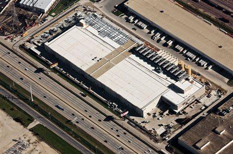
101 101

102 102
103 Thank You! Ques>ons? Picture slideshow available at (along with photo credits) 103
104 104
105 Photo credits Slide 6 hqp:// Slide 7 hqp:// 7 Slide 8 hqp:// 8 Slide 9 hqp:// by- Natural/viruses.html 9 Slide 10 hqp:// 10 Slide 11 hqp:// 11 Slide 12 12
106 Photo credits Slide 13 hqp:// 13 Slide 14 1 mm hqp:// 14 Slide mm = 500 um hqp://zphotoblog.com/maths- close- up- of- the- pencil/ 15 Slide 16 Human hair 100 um hqp:// 16 Slide um pixel size in the iphone 4 as small as the eye can see hqp://blog.demandware.com/blog/?tag=forrester 17
107 Photo credits Slide 18 Pollen spores typical 10 um hqp:// 18 Slide 19 Bacteria typically 1 um in size SEM image of Methicillin- Resistant Staphylococcus aureus (MRSA) Kills about 100,000 people in USA each year hqp:// Slide 20 hqp:// 20 Slide 21 AIDS virus typical size 100 nm hqp://001yourtransla>onservice.com/computer- >ps/protec>ng- your- computer.htm 21 Slide 22 Atomic dimensions typically 1 nm hqp://flack13.blogspot.com/2008_06_01_archive.html22 Slide 23 Nano Par>cles in our Environment23 Slide 24 hqp://rst.gsfc.nasa.gov/sect16/sect16_1.html 24
108 Photo credits Slide 25 hqp://livinggreenadvice.com/blog/environment/what s- in- that- spray- can- you re- holding/ 25 Slide 26 Each breath: millions of nanopar>cles, typical size 10 nm hqp:// content/uploads/2010/03/mexico- city- air- britain1.jpg 26 Slide 27 hqp://volcano- pictures.info/glossary/pyroclas>c_flow.html 27 Slide 28 hqp://candlefind.com/candle- reviews/julia- wooten/emily- s- candles- bath.html 28 Slide Slide 30 hqp:// 30 Slide 31 hqp:// 31 Slide 32 hqp:// 32
109 Photo credits Slide 33 hqp:// 33 Slide 34 hqp:// 34 Slide 35 hqp:// 35 Slide 36 hqp:// 36 Slide 37 hqp:// 37 Slide 38 hqp://crazy- frankenstein.com/the- chip- that- is- changing- our- lives.html38 Slide and P2 hqp://hlhsos.com/ hqp://
110 Photo credits Slide Slide 41 JM - Excel41 Slide 42 hqp:// 42 Slide 43 hqp:// 43 Slide 44 hqp://memory- card- recovery.org/tag/flash- data- recovery 44 Slide 45 Slide 46 Slide 47 hqp:// 47 Slide 48 hqps://infosecurity.us/?p=
111 Photo credits Slide 49 Microsos data center hqp://blogs.technet.com/b/msdatacenters/archive/2009/06/29/microsos- brings- two- more- mega- data- centers- online- in- july.aspx 49 Slide 50 Google data center hqp://sciencelife.uchospitals.edu/wp- content/uploads/googe- datacenter- 300x225.jpg 50 Slide 51 hqp:// 51 Slide 52 Cisco CRS- 3: 322 Tbps router, e hqp:// crs- 3- can- deliver- every- movie- ever- made- in- 4- minutes/52 Slide 53 hqp://blogs.cornell.edu/newmedia10blb45/ 53 Slide Slide 55 hqp:// 55 Slide 56 hqp://en.wikipedia.org/wiki/file:evg- 620_%26_MA- 150_steppers_at_LAAS_(FDLS_2007)_0438.jpg 56 Slide 57 SEM: hqp://en.wikipedia.org/wiki/file:ernst_ruska_electron_microscope_- _Deutsches_Museum_- _Munich- edit.jpg SEM: hqp://
112 Photo credits Slide 49 Microsos data center hqp://blogs.technet.com/b/msdatacenters/archive/2009/06/29/microsos- brings- two- more- mega- data- centers- online- in- july.aspx 49 Slide 50 Google data center hqp://sciencelife.uchospitals.edu/wp- content/uploads/googe- datacenter- 300x225.jpg 50 Slide 51 hqp:// 51 Slide 52 Cisco CRS- 3: 322 Tbps router, e hqp:// crs- 3- can- deliver- every- movie- ever- made- in- 4- minutes/52 Slide 53 hqp://blogs.cornell.edu/newmedia10blb45/ 53 Slide Slide 55 hqp:// 55 Slide 56 hqp://en.wikipedia.org/wiki/file:evg- 620_%26_MA- 150_steppers_at_LAAS_(FDLS_2007)_0438.jpg 56 Slide 57 SEM: hqp://en.wikipedia.org/wiki/file:ernst_ruska_electron_microscope_- _Deutsches_Museum_- _Munich- edit.jpg SEM: hqp://
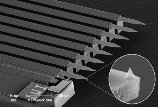
113 Photo credits Slide 58 Ebeam lithography (EBL), PECVD, spuqerer, focused ion beam (FIB) (hqp:// ebeam.html) EBL highest resolu>on (20 n) but slow PECVD great control over morphology (hqp:// SpuQerer (hqp:// FIB beam of metal atoms, used to mill surfaces (ion milling) (hqp:// Slide 59 SEM: hqp://science.howstuffworks.com/scanning- electron- microscope.htm/printable59 Slide 60 Human blood (hqp://en.wikipedia.org/wiki/file:sem_blood_cells.jpg) ant s head (hqp:// Slide 61 Surface of a computer chip (hqp://users.elis.ugent.be/~aldevos/projects/computer.html)61 Slide 62 scanning tunneling microscope [STM], which was invented in 1981 by Gerd Binnig and Heinrich Rohrer, both employed by I.B.M. Research in Zurich. Binnig and Rohrer won the 1986 Nobel Prize in physics for their inven>on (hqp://mcff.mtu.edu/ acmal/images/veecodim3000afm.jpg)62 Slide 63 AFM (hqp:// Slide 64 AFM >p photo Frankel (hqp://pubs.acs.org/cen/books/88/8807books.html)64 Slide 65 AFM >ps (hqp://
114 Photo credits Slide 66 AFM opera>on (hqp://www3.physik.uni- greifswald.de/method/afm/eafm.htm)66 Slide 67 Si(111) 7x7 problem solved by STM (hqp:// index.html~omicron)67 Slide 68 Famous use of STM to resolve Si(111) 7x7 reconstruc>on problem (hqp:// rom/highly_resolved_stm/index.html~omicron)68 Slide 69 Constant current STM image of a GaAs (110) surface highly doped with Zn acceptors at T = 4.7 K. (hqp:// Slide 70 quantum corrals made of Fe atoms on Cu(111) surface Shapes inside due to electrons in Cu surface bouncing in paqern hqp:// sciences.com/fr/news/t/physique- 1/d/ibm- poursuit- sa- conquete- du- nanomonde_14714/ 70 Slide 71 PT(100) surface and reconstruc>on hqp:// 71
115 Photo credits Slide 72 Interplay between imaging and simula>ons! Low- coverage EDOT molecules on Cu(110) self- organize into stacks hqp:// 72 Slide 73 Sos maqer AFM lipid bilayer hqp:// 73 Slide 74 AFM e- coli 1x2 um hqp:// 74 Slide 75 AFM, Magne>c Force Microscopy (MFM) hard disk surface hqp:// 75 Slide 76 Eigler and Schweizer 1990 hqp:// 76
116 Photo credits Slide Slide 78 MEMS hqp:// 78 Slide 79 MEMS hqp:// 79 Slide 80 MEMS (hqp:// Drexler) 80 Slide 81 MEMS hqp:// 81 Slide 82 hqp://en.wikipedia.org/wiki/mems 82 Slide 83 Texas Instruments Digital Light Processor (DLP) chip hqp:// kiel.de/matwis/amat/semitech_en/kap_7/backbone/r7_1_1.html 83
117 Photo credits Slide 84 Opera>on of DLP projector hqp:// 84 Slide Slide 86 Buckeyball 60 carbon atoms, about 1 nm in diameter nanohub.org Lots of other carbon allotropes hqp://
118 Photo credits Slide 87 Nanotubes are very strong hqp://en.wikipedia.org/wiki/carbon_nanotube87 Slide 88 Pillared graphene consists of CNTs and graphene sheets combined to form a 3D network nanostructure hqp://spie.org/x33929.xml?ar>cleid=x Slide 89 Lots of carbon nanostructures are contained in soot hqp://candlefind.com/candle- reviews/julia- wooten/emily- s- candles- bath.html 89 Slide Slide 91 Langmuir- BlodgeQ film hqp://en.wikipedia.org/wiki/langmuir%e2%80%93blodgeq_film Pulling an LB film from a trough hqp://en.wikipedia.org/wiki/langmuir- BlodgeQ_trough
119 Photo credits Slide 92 WeQability provides a way to directly visualize the effects of a molecularly thin layers of molecules on a surface Fully we{ng, par>ally we{ng (hydrophilic), par>al we{ng (hydrophobic), non- we{ng92 Slide 93 Popular as ScotchGaurd stain- resistant fabric coa>ngs (essen>ally a molecular layer of teflon) hqp:// 93 Slide 94 Aquapel or RainEx also give a non- we{ng layer for beqer vision in the rain _ This is some of my background! hqp:// 94 Slide Slide 96 The possibili>es are amazing hqp:// hpp.com/eng/service/pressarchive.php?pm=ct_pm hqp:// 96
120 Photo credits Slide 97 Stem cell research for cancer treatments 97 Slide 98 Advanced imaging hqp://repairstemcell.wordpress.com/2009/02/23/ 98 Slide 99 An>- bacterial coa>ngs on consumer products silver atoms hqp://gizmodo.com/192732/elecom- m+abur- series- usb- mouse- an>bacterial- coa>ng- but- dont- kid- yourself 99 Slide Slide 101 Lots of science fic>on out there! hqp://escuadrondelaverdad.wordpress.com/category/salud/page/2/ 101 Slide 102 More science fic>on? hqp://io9.com/ /where- are- my- medical- nanobots
Nanotechnology, the infrastructure, and IBM s research projects
 Nanotechnology, the infrastructure, and IBM s research projects Dr. Paul Seidler Coordinator Nanotechnology Center, IBM Research - Zurich Nanotechnology is the understanding and control of matter at dimensions
Lecture 20: Optical Tools for MEMS Imaging
 MECH 466 Microelectromechanical Systems University of Victoria Dept. of Mechanical Engineering Lecture 20: Optical Tools for MEMS Imaging 1 Overview Optical Microscopes Video Microscopes Scanning Electron
PH880 Topics in Physics
 PH880 Topics in Physics Modern Optical Imaging (Fall 2010) Overview of week 12 Monday: FRET Wednesday: NSOM Förster resonance energy transfer (FRET) Fluorescence emission i FRET Donor Acceptor wikipedia
Innovative Technology for Innovative Science Hands-on in a Nanoscience Classroom
 Innovative Technology for Innovative Science Hands-on in a Nanoscience Classroom Presented by Jennifer F. Wall, Ph.D. Imaging Possibilities Optical 2 mm Electron 500 microns Atomic Force 10 microns Scanning
write-nanocircuits Direct-write Jaebum Joo and Joseph M. Jacobson Molecular Machines, Media Lab Massachusetts Institute of Technology, Cambridge, MA
 Fab-in in-a-box: Direct-write write-nanocircuits Jaebum Joo and Joseph M. Jacobson Massachusetts Institute of Technology, Cambridge, MA April 17, 2008 Avogadro Scale Computing / 1 Avogadro number s? Intel
Advanced Nanoscale Metrology with AFM
 Advanced Nanoscale Metrology with AFM Sang-il Park Corp. SPM: the Key to the Nano World Initiated by the invention of STM in 1982. By G. Binnig, H. Rohrer, Ch. Gerber at IBM Zürich. Expanded by the invention
Introduction of New Products
 Field Emission Electron Microscope JEM-3100F For evaluation of materials in the fields of nanoscience and nanomaterials science, TEM is required to provide resolution and analytical capabilities that can
Microscopy Techniques that make it easy to see things this small.
 Microscopy Techniques that make it easy to see things this small. What is a Microscope? An instrument for viewing objects that are too small to be seen easily by the naked eye. Dutch spectacle-makers Hans
IBM Research - Zurich Research Laboratory
 October 28, 2010 IBM Research - Zurich Research Laboratory Walter Riess Science & Technology Department IBM Research - Zurich wri@zurich.ibm.com Outline IBM Research IBM Research Zurich Science & Technology
Scale. A Microscope s job in life. The Light Microscope. The Compound Microscope 9/24/12. Compound Microscope Anatomy
 The Study of Microbial Structure: Microscopy and Specimen Preparation Scale A Microscope s job in life 1.Magnify 2. Resolve ability to separate or distinguish between two points 3. Contrast How much or
UNIT 12 : NANO TECHNOLOGY
 UNIT 12 : NANO TECHNOLOGY What is nanotechnology? How was nanotechnology developed? What are the benefits of this kind of technology? Why is it important in our everyday lives? Can you name a product using
Chapter 3. Observing Microorganisms Through a Microscope
 Chapter 3 Observing Microorganisms Through a Microscope Microbial Size Macroscopic organisms can be measured in the range from meters (m) to centimeters (cm) Microscopic organisms fall into the range
The Department of Advanced Materials Engineering. Materials and Processes in Polymeric Microelectronics
 The Department of Advanced Materials Engineering Materials and Processes in Polymeric Microelectronics 1 Outline Materials and Processes in Polymeric Microelectronics Polymeric Microelectronics Process
Micro- and Nano- Fabrication and Replication Techniques
 Micro- and Nano- Fabrication and Replication Techniques Why do we have to write thing small and replicate fast? Plenty of Room at the Bottom Richard P. Feynman, December 1959 How do we write it? We have
Observing Microorganisms through a Microscope LIGHT MICROSCOPY: This type of microscope uses visible light to observe specimens. Compound Light Micros
 PHARMACEUTICAL MICROBIOLOGY JIGAR SHAH INSTITUTE OF PHARMACY NIRMA UNIVERSITY Observing Microorganisms through a Microscope LIGHT MICROSCOPY: This type of microscope uses visible light to observe specimens.
Investigating the Electronic Behavior of Nano-materials From Charge Transport Properties to System Response
 Investigating the Electronic Behavior of Nano-materials From Charge Transport Properties to System Response Amit Verma Assistant Professor Department of Electrical Engineering & Computer Science Texas
CMOL: Hybrid of CMOS with Overlaid Nanogrid and Nanodevice Structure. John Zacharkow
 CMOL: Hybrid of CMOS with Overlaid Nanogrid and Nanodevice Structure John Zacharkow Overview Introduction Background CMOS Review CMOL Breakdown Benefits/Shortcoming Looking into the Future Introduction
DTU DANCHIP an open access micro/nanofabrication facility bridging academic research and small scale production
 DTU DANCHIP an open access micro/nanofabrication facility bridging academic research and small scale production DTU Danchip National Center for Micro- and Nanofabrication DTU Danchip DTU Danchip is Denmark
INTRO TO NANOTECHNOLOGY AND BIOSENSORS 5E Inquiry Lesson Plans - Grades 7-12 Lesson Plan #2: Intro to Nanotechnology & its current uses!
 INTRO TO NANOTECHNOLOGY AND BIOSENSORS 5E Inquiry Lesson Plans - Grades 7-12 Lesson Plan #2: Intro to Nanotechnology & its current uses! ENGAGE: Get out a meter stick. Have students volunteer all the prefixes
A Brief Introduction to Single Electron Transistors. December 18, 2011
 A Brief Introduction to Single Electron Transistors Diogo AGUIAM OBRECZÁN Vince December 18, 2011 1 Abstract Transistor integration has come a long way since Moore s Law was first mentioned and current
Selected Topics in Nanoelectronics. Danny Porath 2002
 Selected Topics in Nanoelectronics Danny Porath 2002 Links to NST http://www.foresight.org/ http://itri.loyola.edu/nanobase/ http://www.zyvex.com/nano/ http://www.nano.gov/ http://www.aeiveos.com/nanotech/
Welcome to. A facility within the Nanometer Structure Consortium (nmc) at Lund University. nanolab. lund
 at Lund University. nanolab. lund") lund nanolab Welcome to A facility within the Nanometer Structure Consortium (nmc) at Lund University »It s a dream come true. This is the lab I always dreamt of. I didn t know it would ever exist.«ivan
lund nanolab Welcome to A facility within the Nanometer Structure Consortium (nmc) at Lund University »It s a dream come true. This is the lab I always dreamt of. I didn t know it would ever exist.«ivan
Microscopy. ( greek mikros = small; skopein = to observe)
") Microscopy ( greek mikros = small; skopein = to observe) Zacharias Jansen put several lenses in a tube (first compound microscope) and the object near the end of tube appeared to be greatly enlarged, much
Microscopy ( greek mikros = small; skopein = to observe) Zacharias Jansen put several lenses in a tube (first compound microscope) and the object near the end of tube appeared to be greatly enlarged, much
CHAPTER 6 CARBON NANOTUBE AND ITS RF APPLICATION
 CHAPTER 6 CARBON NANOTUBE AND ITS RF APPLICATION 6.1 Introduction In this chapter we have made a theoretical study about carbon nanotubes electrical properties and their utility in antenna applications.
ASCENT Overview. European Nanoelectronics Infrastructure Access. MOS-AK Workshop, Infineon, Munich, 13 th March 2018.
 ASCENT Overview MOS-AK Workshop, Infineon, Munich, 13 th March 2018 European Nanoelectronics Infrastructure Access Paul Roseingrave The Challenge Cost/performance returns by scaling are diminishing Cost
Unit-25 Scanning Tunneling Microscope (STM)
") Unit-5 Scanning Tunneling Microscope (STM) Objective: Imaging formation of scanning tunneling microscope (STM) is due to tunneling effect of quantum physics, which is in nano scale. This experiment shows
Unit-5 Scanning Tunneling Microscope (STM) Objective: Imaging formation of scanning tunneling microscope (STM) is due to tunneling effect of quantum physics, which is in nano scale. This experiment shows
Opportunities and Challenges for Nanoelectronic Devices and Processes
 The Sixth U.S.-Korea Forum on Nanotechnology, April 28-29, 2009, Las Vegas, NV Opportunities and Challenges for Nanoelectronic Devices and Processes Yoshio Nishi Professor, Electrical Engineering, Material
Virtual Scanning Tunneling Microscope Offered as a Free-Download
 Mark Hagmann*, Greg Spencer, and Jeremy Wiedemeier NewPath Research L.L.C., 2880 S. Main St., Ste. 214, Salt Lake City, UT 84115 *newpathresearch@gmail.com Abstract: The scanning tunneling microscope is
The Future of Technology
 Technology And Society Committee November 11, 2008 Slides: http://www.slideshare.net/lablogga/slideshows Melanie Swan Research Associate MS Futures Group Palo Alto, CA 415-505-4426 m@melanieswan.com http://www.melanieswan.com
New Process Technologies Will silicon CMOS carry us to the end of the Roadmap?
 HPEC Workshop 2006 New Process Technologies Will silicon CMOS carry us to the end of the Roadmap? Craig L. Keast, Chenson Chen, Mike Fritze, Jakub Kedzierski, Dave Shaver HPEC 2006-1 Outline A brief history
Introduction to Electron Microscopy
 Introduction to Electron Microscopy Prof. David Muller, dm24@cornell.edu Rm 274 Clark Hall, 255-4065 Ernst Ruska and Max Knoll built the first electron microscope in 1931 (Nobel Prize to Ruska in 1986)
Chapter 2 The Study of Microbial Structure: Microscopy and Specimen Preparation
 Chapter 2 The Study of Microbial Structure: Microscopy and Specimen Preparation 1 Lenses and the Bending of Light light is refracted (bent) when passing from one medium to another refractive index a measure
A Project Report Submitted to the Faculty of the Graduate School of the University of Minnesota By
 Observation and Manipulation of Gold Clusters with Scanning Tunneling Microscopy A Project Report Submitted to the Faculty of the Graduate School of the University of Minnesota By Dogukan Deniz In Partial
GLOBAL MARKETS, TECHNOLOGIES AND MATERIALS FOR THIN AND ULTRATHIN FILMS
 GLOBAL MARKETS, TECHNOLOGIES AND MATERIALS FOR THIN AND ULTRATHIN FILMS SMC057C August Margareth Gagliardi Project Analyst ISBN: 1-62296-338-5 BCC Research 49 Walnut Park, Building 2 Wellesley, MA 02481
IBM Research Zurich. A Strategy of Open Innovation. Dr. Jana Koehler, Manager Business Integration Technologies. IBM Research Zurich
 IBM Research Zurich A Strategy of Open Innovation Dr., Manager Business Integration Technologies IBM A Century of Information Technology Founded in 1911 Among the leaders in the IT industry in every decade
All-Glass Gray Scale PhotoMasks Enable New Technologies. Che-Kuang (Chuck) Wu Canyon Materials, Inc.
 Wu Canyon Materials, Inc.") All-Glass Gray Scale PhotoMasks Enable New Technologies Che-Kuang (Chuck) Wu Canyon Materials, Inc. 1 Overview All-Glass Gray Scale Photomask technologies include: HEBS-glasses and LDW-glasses HEBS-glass
All-Glass Gray Scale PhotoMasks Enable New Technologies Che-Kuang (Chuck) Wu Canyon Materials, Inc. 1 Overview All-Glass Gray Scale Photomask technologies include: HEBS-glasses and LDW-glasses HEBS-glass
Optical Microscope. Active anti-vibration table. Mechanical Head. Computer and Software. Acoustic/Electrical Shield Enclosure
 Optical Microscope On-axis optical view with max. X magnification Motorized zoom and focus Max Field of view: mm x mm (depends on zoom) Resolution : um Working Distance : mm Magnification : max. X Zoom
Metrology and Nanotechnology in Interrelation with Intellectual Property Rights
 Metrology and Nanotechnology in Interrelation with Intellectual Property Rights L. Kräuter, M.N. Durakbasa, P.H Osanna Department for Interchangeable Manufacturing and Industrial Metrology Vienna University
CHAPTER 1 INTRODUCTION. the sectors of industrial and customer products [5]. The first ever concept of nanotechnology
![CHAPTER 1 INTRODUCTION. the sectors of industrial and customer products [5]. The first ever concept of nanotechnology](/thumbs/86/94425600.jpg "CHAPTER 1 INTRODUCTION. the sectors of industrial and customer products [5]. The first ever concept of nanotechnology") CHAPTER 1 INTRODUCTION 1.1 General Introduction: Nanotechnology is defined as the application of nanoscience in technological devices/processes/products. It is fast promising technology capable of impacting
CHAPTER 1 INTRODUCTION 1.1 General Introduction: Nanotechnology is defined as the application of nanoscience in technological devices/processes/products. It is fast promising technology capable of impacting
MICROSCOPES. Magnification: Resolution: Field of View: Describes the visual picture seen when looking through the eyepiece of the microscope
 Microscopes MICROSCOPES Magnification: Resolution: Field of View: Describes the visual picture seen when looking through the eyepiece of the microscope 7X 45X 112.5X 225X 1 st crude microscope made by
NANOELECTRONIC TECHNOLOGY: CHALLENGES IN THE 21st CENTURY
 NANOELECTRONIC TECHNOLOGY: CHALLENGES IN THE 21st CENTURY S. M. SZE National Chiao Tung University Hsinchu, Taiwan And Stanford University Stanford, California ELECTRONIC AND SEMICONDUCTOR INDUSTRIES
Microbiology: Observing Bacteria Laboratory -1. Name Date
 Microbiology: Observing Bacteria Laboratory -1 Name Date Prelab: Part 1 Introduction to the microscope- please read through this handout and label the picture on the next page before starting the lab Care
Introduction to Materials Engineering: Materials Driving the Electronics Revolution Robert Hull, MSE
 Introduction to Materials Engineering: Materials Driving the Electronics Revolution Robert Hull, MSE Outline Microelectronics Miniaturization Historical Development: Electronics before Semiconductors The
Low-energy Electron Diffractive Imaging for Three dimensional Light-element Materials
 Low-energy Electron Diffractive Imaging for Three dimensional Light-element Materials Hitachi Review Vol. 61 (2012), No. 6 269 Osamu Kamimura, Ph. D. Takashi Dobashi OVERVIEW: Hitachi has been developing
MICROSCOPE TERMS 7X 45X 112.5X 225X
 Microscopes MICROSCOPE TERMS Magnification- how much larger the image is Resolution- how clear the image is Field of View: Describes the visual picture seen when looking through the eyepiece of the microscope
International Center on Design for Nanotechnology Workshop August, 2006 Hangzhou, Zhejiang, P. R. China
 Challenges and opportunities for Designs in Nanotechnologies International Center on Design for Nanotechnology Workshop August, 2006 Hangzhou, Zhejiang, P. R. China Sankar Basu Program Director Computing
Enabling Breakthroughs In Technology
 Enabling Breakthroughs In Technology Mike Mayberry Director of Components Research VP, Technology and Manufacturing Group Intel Corporation June 2011 Defined To be defined Enabling a Steady Technology
IH2655 Design and Characterisation of Nano- and Microdevices. Lecture 1 Introduction and technology roadmap
 IH2655 Design and Characterisation of Nano- and Microdevices Lecture 1 Introduction and technology roadmap IH2655 Design and Characterisation of Nano- and Microdevices Introduction to IH2655 Brief historic
Low Voltage Electron Microscope
 LVEM5 Low Voltage Electron Microscope Nanoscale from your benchtop LVEM5 Delong America DELONG INSTRUMENTS COMPACT BUT POWERFUL The LVEM5 is designed to excel across a broad range of applications in material
NanoFabrication Kingston. Seminar and Webinar January 31, 2017 Rob Knobel Associate Professor, Dept. of Physics Queen s University
 NanoFabrication Kingston Seminar and Webinar January 31, 2017 Rob Knobel Associate Professor, Dept. of Physics Queen s University What is NFK? It s a place, an team of experts and a service. The goal of
Ex 1: Introduction to the microscope
 Ex 1: Introduction to the microscope So what exactly is a microorganism? Microorganisms = any living thing that is too small to be seen with the unaided eye fungus protist bacteria virus Parasitic worm
LAB UNIT 1: Introduction Scanning Force Microscopy
 LAB UNIT 1: Introduction Specific Assignment: Setup of scanning force microscopy experiment and first contact measurements Objective Outcome Synopsis The student will become familiar with contact mode
Introduction to Microdevices and Microsystems
 PHYS 534 (Fall 2008) Module on Microsystems & Microfabrication Lecture 1 Introduction to Microdevices and Microsystems Srikar Vengallatore, McGill University 1 Introduction to Microsystems Outline of Lecture
MEMS for RF, Micro Optics and Scanning Probe Nanotechnology Applications
 MEMS for RF, Micro Optics and Scanning Probe Nanotechnology Applications Part I: RF Applications Introductions and Motivations What are RF MEMS? Example Devices RFIC RFIC consists of Active components
Class Website: p b2008.htm
 EEE598 Molecular Electronics Some Information about the Course Instructor: Dr. Nongjian Tao (njtao@asu.edu) Where: ECA 219 When: TTH 12:00 1:15 pm Office Hours: TTH 1:30-2:30 p.m. or by appointment. Office
NNIN Nanotechnology Education
 NNIN Nanotechnology Education Student Worksheet Learning Set on Size, Scale, Function, and Measurement Systems Name: Date: Does Size Matter? Individual View Imagine that scientists have the ability to
Observing Microorganisms through a Microscope
 2016/2/19 PowerPoint Lecture Presentations prepared by Bradley W. Christian, McLennan Community College CHAPTER 3 Observing Microorganisms through a Microscope 1 Figure 3.2 Microscopes and Magnification.
LOW LEAKAGE CNTFET FULL ADDERS
 LOW LEAKAGE CNTFET FULL ADDERS Rajendra Prasad Somineni srprasad447@gmail.com Y Padma Sai S Naga Leela Abstract As the technology scales down to 32nm or below, the leakage power starts dominating the total
Fabrication of Probes for High Resolution Optical Microscopy
 Fabrication of Probes for High Resolution Optical Microscopy Physics 564 Applied Optics Professor Andrès La Rosa David Logan May 27, 2010 Abstract Near Field Scanning Optical Microscopy (NSOM) is a technique
Nanovie. Scanning Tunnelling Microscope
 Nanovie Scanning Tunnelling Microscope Nanovie STM Always at Hand Nanovie STM Lepto for Research Nanovie STM Educa for Education Nanovie Auto Tip Maker Nanovie STM Lepto Portable 3D nanoscale microscope
Low Voltage Electron Microscope. Nanoscale from your benchtop LVEM5. Delong America
 LVEM5 Low Voltage Electron Microscope Nanoscale from your benchtop LVEM5 Delong America DELONG INSTRUMENTS COMPACT BUT POWERFUL The LVEM5 is designed to excel across a broad range of applications in material
Laser patterning and projection lithography
 Introduction to Nanofabrication Techniques: Laser patterning and projection lithography Benjamin Johnston Macquarie University David O Connor Bandwidth Foundry - USYD The OptoFab node of ANFF Broad ranging
Introduction to Optoelectronic Devices
 Introduction to Optoelectronic Devices Dr. Jing Bai Assistant Professor Department of Electrical and Computer Engineering University of Minnesota Duluth October 30th, 2012 1 Outline What is the optoelectronics?
January, 2004 Jeju Island. Acknowledgements OTFL
 High-Speed Fabrication of Nanostructures using Atomic Force Microscope Lithography Haiwon Lee Department of Chemistry US-Korea NanoForum 02/17, 2005 January, 2004 Jeju Island Acknowledgements Contents
SEMINAR ON PERSPECTIVES OF NANOTECHNOLOGY FOR RF AND TERAHERTZ ELECTRONICS. February 1, 2013
 SEMINAR ON PERSPECTIVES OF NANOTECHNOLOGY FOR RF AND TERAHERTZ ELECTRONICS February 1, 2013 GuideMr.Harikrishnan A.IAsst ProfessorANJUSEMINAR MICHAEL ONPERSPECTIVES (NSAJEEC013) OF NANOTECHNOLOGY FOR February
Burton's Microbiology for the Health Sciences
 Burton's Microbiology for the Health Sciences Chapter 2. Viewing the Microbial World Chapter 2 Outline Introduction Using the metric system to express the sizes of microbes Microscopes Simple microscopes
The microscope is useful in making observations and collecting data in scientific experiments. Microscopy involves three basic concepts:
 AP BIOLOGY Chapter 6 NAME DATE Block MICROSCOPE LAB PART I: COMPOUND MICROSCOPE OBJECTIVES: After completing this exercise you should be able to: Demonstrate proper care and use of a compound microscope.
Ion Beam Lithography: faster writing strategies for features between 150nm and 1um
 Ion Beam Lithography: faster writing strategies for features between 150nm and 1um Brent P. Gila, Andes Trucco, David Hays Located in sunny Gainesville, FL (100 miles north of Disney World) https://nrf.aux.eng.ufl.edu/
AST 443 / PHY 517. Photon Detectors
 AST 443 / PHY 517 Photon Detectors Photons Light is electro- magne>c radia>on Crossed electric and magne>c vectors Self- propaga>ng Travels at speed of light c c=2.99792 x 10 8 m/s (vacuum) λν = c n=c/v
Smaller than the eye can see: How your computer is made June 19, 2006
 Smaller than the eye can see: How your computer is made June 19, 2006 Agenda for today: 1) Getting to know each other/taking pictures (Mark) 2) Overview of the next three weeks (Mark) 3) Keeping a laboratory
Energy beam processing and the drive for ultra precision manufacturing
 Energy beam processing and the drive for ultra precision manufacturing An Exploration of Future Manufacturing Technologies in Response to the Increasing Demands and Complexity of Next Generation Smart
Scanning Tunneling Microscopy
 Scanning Tunneling Microscopy The wavelike properties of electrons allows them to tunnel beyond the regions of a solid into a region of space forbidden for them to exist in. In this region they can be
Microscope Notes. units of life.
 Microscope Notes Microscope an instrument that produces an enlarged image of an object. Biologists use microscopes to study cells, cell parts, and organisms that are too small to be seen with the naked
Status and Challenges for Probe Nanopatterning. Urs Duerig, IBM Research - Zurich
 Status and Challenges for Probe Nanopatterning Urs Duerig, IBM Research - Zurich Mask-less Lithography Electron beam lithography de-facto industry standard Probe lithography mainly a research tool Courtesy
C h e m i st r y C o n n e ct s to Te chn olo gy
 Real Science-4-Kids C h e m i st r y C o n n e ct s to Te chn olo gy Workbook Level I A Rebecca W. Keller, Ph.D. Cover design: David Keller Opening page: David Keller Illustrations: Janet Moneymaker, Rebecca
THE FEYNMAN ANNIVERSARY SYMPOSIUM
 THE FEYNMAN ANNIVERSARY SYMPOSIUM 12 & 13 February 2010 at the University of South Carolina. sponsored by the South Carolina Honors College (Dr. Davis Baird, Dean) and the USC NanoCenter (Dr. Tom Vogt,
POLYMER MICROSTRUCTURE WITH TILTED MICROPILLAR ARRAY AND METHOD OF FABRICATING THE SAME
 POLYMER MICROSTRUCTURE WITH TILTED MICROPILLAR ARRAY AND METHOD OF FABRICATING THE SAME Field of the Invention The present invention relates to a polymer microstructure. In particular, the present invention
- Near Field Scanning Optical Microscopy - Electrostatic Force Microscopy - Magnetic Force Microscopy
 - Near Field Scanning Optical Microscopy - Electrostatic Force Microscopy - Magnetic Force Microscopy Yongho Seo Near-field Photonics Group Leader Wonho Jhe Director School of Physics and Center for Near-field
Education and Outreach: Nanotechnology Activity Guides
 Education and Outreach: Nanotechnology Activity Guides Rocks and Nanobots: A Societal Interaction Impact Lab Audience: Middle school class to graduate student class Time Needed: Activity 1 10-15 minutes
Electron
 Electron 1897: Sir Joseph John Thomson (1856-1940) discovered corpuscles small particles with a charge-to-mass ratio over 1000 times greater than that of protons. Plum pudding model : electrons in a sea
Triple i - The key to your success
 Triple i - The key to your success The needs and challenges of today s world are becoming ever more demanding. Standards are constantly rising. Creativity, reliability and high performance are basic prerequisites
Nanosurf easyscan 2 Your Modular Scanning Probe Microscopy System
 Nanosurf Your Modular Scanning Probe Microscopy System www.nanosurf.com Perfect Modularity Nanosurf s easyscan series has gained worldwide popularity through its affordability, portability, and ease of
Introduction to Electronic Devices
 (Course Number 300331) Fall 2006 Instructor: Dr. Dietmar Knipp Assistant Professor of Electrical Engineering Information: http://www.faculty.iubremen.de/dknipp/ Source: Apple Ref.: Apple Ref.: IBM Critical
Scanning Tunneling Microscopy
 EMSE-515 02 Scanning Tunneling Microscopy EMSE-515 F. Ernst 1 Scanning Tunneling Microscope: Working Principle 2 Scanning Tunneling Microscope: Construction Principle 1 sample 2 sample holder 3 clamps
Norsam Technologies, Inc. Ultra-High Density Analog and Digital Data Storage
 Norsam Technologies, Inc. Ultra-High Density Analog and Digital Data Storage Digital and Analog Technology HD-ROM Charged particle technology HD-Rosetta Norsam HD-Rosetta Technology A complete solution
Georgia Tech IEN EBL Facility NNIN Highlights 2014 External User Projects
 Georgia Tech IEN EBL Facility NNIN Highlights 2014 External User Projects Silicon based Photonic Crystal Devices Silicon based photonic crystal devices are ultra-small photonic devices that can confine
Nanostencil Lithography and Nanoelectronic Applications
 Microsystems Laboratory Nanostencil Lithography and Nanoelectronic Applications Oscar Vazquez, Marc van den Boogaart, Dr. Lianne Doeswijk, Prof. Juergen Brugger, LMIS1 Dr. Chan Woo Park, Visiting Professor
High Resolution Imaging of Nanoscale Structures by Scanning Probe Microscopy Techniques
 High Resolution Imaging of Nanoscale Structures by Scanning Probe Microscopy Techniques Prof. Marco Farina, Senior Member IEEE Dipartimento di Ingegneria dell Informazione Università Politecnica delle
School Field Trip Framework
 School Field Trip Framework Organization: Sciencenter Contact person: Kevin Dilley Contact information: kdilley@sciencenter.org General Description Audience: School group of students ages 8 to 11 year
Plasmonic Metamaterials and Optical Holography ( 全息术 )
") Plasmonic Metamaterials and Optical Holography ( 全息术 ) Guixin Li ( 李贵新 ) Department of Physics, Faculty of Science Hong Kong Baptist University 28 th April 2015 Light-Matter Interactions Target Advanced
Plasmonic Metamaterials and Optical Holography ( 全息术 ) Guixin Li ( 李贵新 ) Department of Physics, Faculty of Science Hong Kong Baptist University 28 th April 2015 Light-Matter Interactions Target Advanced
INDUSTRIAL TECHNOLOGIES FOR SCHOOLS
 INDUSTRIAL TECHNOLOGIES FOR SCHOOLS (LMS) Director: Prof. George Chryssolouris Dept. of Mechanical Engineering & Aeronautics University of Patras, Greece INDUSTRIAL TECHNOLOGIES FOR SCHOOLS: BACKGROUND
Advances in Materials Science and Engineering
 Review Article Advances in Materials Science and Engineering Optimized Ordered Nanoprinting Using Focused Ion Beam Lama Mahmoud Department of Mechanical and Materials Science and Engineering, Khalifa University,
Triple Beam FIB-SEM-Ar(Xe) Combined System NX2000
 Combined System NX2000") SCIENTIFIC INSTRUMENT NEWS 2017 Vol. 8 M A R C H Technical magazine of Electron Microscope and Analytical Instruments. Technical Explanation Triple Beam FIB-SEM-Ar(Xe) Combined System NX2000 Masahiro Kiyohara
SCIENTIFIC INSTRUMENT NEWS 2017 Vol. 8 M A R C H Technical magazine of Electron Microscope and Analytical Instruments. Technical Explanation Triple Beam FIB-SEM-Ar(Xe) Combined System NX2000 Masahiro Kiyohara
EE105 Fall 2015 Microelectronic Devices and Circuits. Invention of Transistors
 EE105 Fall 2015 Microelectronic Devices and Circuits Prof. Ming C. Wu wu@eecs.berkeley.edu 511 Sutardja Dai Hall (SDH) 1-1 Invention of Transistors - 1947 Bardeen, Shockley, and Brattain at Bell Labs Invented
microelectronics services high-tech requires high-precision microelectronics services
 ELECTRICAL & ELECTRONICS microelectronics services high-tech requires high-precision microelectronics services WORLDWIDE Analysis, TESTING & CERTIFICATION LOCALLY AVAILABLE worldwide Electrical and electronic
Author(s) Issue Date Text Version author. DOI / /18/9/095501
 Issue Date Text Version author. DOI / /18/9/095501") Title Author(s) Citation Refinement of Conditions of Point-Contact Current Imaging Atomic Force Microscopy for Molecular-Scale Conduction Measurements Yajima, Takashi; Tanaka, Hirofumi; Matsumoto, Takuya;
Title Author(s) Citation Refinement of Conditions of Point-Contact Current Imaging Atomic Force Microscopy for Molecular-Scale Conduction Measurements Yajima, Takashi; Tanaka, Hirofumi; Matsumoto, Takuya;
Collaboration: The Semiconductor Industry s Path to Survival and Growth
 Collaboration: The Semiconductor Industry s Path to Survival and Growth Dr. Michael R. Polcari President and CEO SEMATECH 15 March 2005 3/17/2005 J:\ADMCTR\OCE\M_Polcari\ITPC 10-04 1 Outline Environment
Monitoring of Galvanic Replacement Reaction. between Silver Nanowires and HAuCl 4 by In-Situ. Transmission X-Ray Microscopy
 Supporting Information Monitoring of Galvanic Replacement Reaction between Silver Nanowires and HAuCl 4 by In-Situ Transmission X-Ray Microscopy Yugang Sun *, and Yuxin Wang Center for Nanoscale Materials
FRAUNHOFER INSTITUTE FOR PHOTONIC MICROSYSTEMS IPMS. Application Area. Quality of Life
 FRAUNHOFER INSTITUTE FOR PHOTONIC MICROSYSTEMS IPMS Application Area Quality of Life Overlay image of visible spectral range (VIS) and thermal infrared range (LWIR). Quality of Life With extensive experience
Zinc Oxide Nanowires Impregnated with Platinum and Gold Nanoparticle for Ethanol Sensor
 CMU. J.Nat.Sci. Special Issue on Nanotechnology (2008) Vol. 7(1) 185 Zinc Oxide Nanowires Impregnated with Platinum and Gold Nanoparticle for Ethanol Sensor Weerayut Wongka, Sasitorn Yata, Atcharawan Gardchareon,