Innovative Technology for Innovative Science Hands-on in a Nanoscience Classroom
|
|
|
- Arline Howard
- 6 years ago
- Views:
Transcription
1 Innovative Technology for Innovative Science Hands-on in a Nanoscience Classroom Presented by Jennifer F. Wall, Ph.D.


2 Imaging Possibilities Optical 2 mm Electron 500 microns Atomic Force 10 microns Scanning Tunneling 5 nm Innovative Technology for Innovative Science 2
3 Hands-on in a Nanoscience Classroom Why Importance of micro and nanotechnologies Hands-on learning How: Complementary tools plus tips from the trade Scanning Electron Microscope (SEM) Atomic Force Microscope (AFM) Scanning Tunneling Microscope (STM) Optical Profiler Where: Nanoscience Classroom Scanning Probe Microscopy Innovative Technology for Innovative Science 3


4 Shrinking scales Why Nanotechnology Molecular and atomic properties Interfaces Micro and nanomanipulation Fundamental principles Product development Innovative Technology for Innovative Science 4


5 Why: Benefits of Hands-on Experiences Give students competitive edge Develop skills: Operation of scientific equipment Critical thinking Laboratory skills Data analysis Problem solving Self-direction Team work Peer learning Apply and retain knowledge Innovative Technology for Innovative Science 5


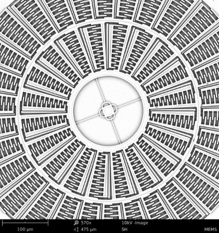
6 How: Classroom Necessities Ease of use Robust Accessible Versatile Affordable Rookie training SEM image of MEMS AFM image of Bluray disk Zeta image of fruit fly head Innovative Technology for Innovative Science 6


7 Why is Scanning Electron Microscopy Important? Advanced Engineering Semiconductors Microelectronics and MEMS Aerospace Solar Filtration Ultrasonic Biometrics Fuel Cells and Battery Green Technology Academic and Government Research Chemistry, physics, material sciences, engineering, biology universal! Life Sciences and Medical Pharmacology Medical devices and implants Bioengineering Cellular and molecular organisms Food sciences Innovative Technology for Innovative Science 7


8 Teaching with an SEM Then Size restrictions Logistics and infrastructure Dedicated personnel Student observation only Time limitations TJHS looking at nerve bundles Now Small footprint Infrastructure not needed Short learning cycle Students can operate No user maintenance Innovative Technology for Innovative Science 8
9 Video Importance of Materials Science and why every school needs a Phenom Full interview with Prof. Sir Colin Humphreys is at Innovative Technology for Innovative Science 9


10 How: Lab Modules for SEM Forensics lab Salt analysis and introduction to close-packing in solids Seed germination analysis Teaching art with the Phenom Crystal growth study Pollen lab to identify allergens Photosynthesis Teaching units with the SEM Simplified manual Simplified sample preparation guide Thanks to D. Moore, Chemeketa College, Univ. of AR, Oregon Museum of Science and Industry Innovative Technology for Innovative Science 10


11 How: SEM in the Lab Biology Biotechnology Biological films on fabric Immunology Forensics Hair, fibers, EDS Materials Science Polymers, ceramics, textiles, Environmental Science Micro-fossils, filtration particles, sand, volcanic ash CSI-style summer program Students prepare and image flagellates, diatoms, cells, and tissue Innovative Technology for Innovative Science 11


12 Why is Scanning Probe Microscopy Important? Surface Manipulation Moving atoms, molecules Lithography Life Science and Medical Targeted drug delivery DNA Cell biology Self-assembled structures Advanced Engineering Semiconductor Microelectronics Thin films Electro-optics Aerospace Ceramics Storage media Polymers Innovative Technology for Innovative Science 12


13 Teaching with an AFM Robust Portable Pre-aligned laser Students can operate No user maintenance Materials Engineering at Bronx CC Innovative Technology for Innovative Science 13


14 How: AFM Sample Kit Chip structure in Silicon CD stamper Gold colloids Nanotubes Glass beads Staphylococus Aureus Microstructure PS/PMMA film Skin cross-section Aluminum foil Innovative Technology for Innovative Science 14


15 Thanks to Prof. Jim Brenner How: AFM in the Lab at FIT Nanotechnology I Laboratory Laboratory Activities with AFM/STM Magnetic ferrofluids CdS and Au nanoparticles CNTs, porous C, nanowires Materials Characterization Laboratory SEM/EDS Mastery Skills TEM Mastery Skills STM Mastery Skills AFM Mastery Skills AFM tracks structural changes of ammonium hydrogen phosphate Innovative Technology for Innovative Science 15

16 How: AFM at Carnegie Mellon PA Governor s School for Sciences program Rigorous selection process High school junior program Use AFM to image live yeast cells Cell structure Effects oxidants and antioxidants Innovative Technology for Innovative Science 16


17 Teaching with an STM Robust Portable Students can operate No user maintenance PChem lab at TX A&M Innovative Technology for Innovative Science 17


18 Why Did the Electron Cross the Road?... How: STM in the Lab HOPG Gold SAM Porphyrins CNT Lab module for SAM courtesy of Dr. C. Sykes at Tufts University HOPG Scan size: 5 nm Au on mica Scan size: 10 mm Octodecanol Scan size: 16 nm Innovative Technology for Innovative Science 18


19 How: AFM and STM in the Lab University of Virginia Three AFMs and 3 STMs for nanoscience lab Molecular self-assembly, DNA scaffolding, microassembly Materials on the web per NSF grant Innovative Technology for Innovative Science 19


20 Why is an Optical Profiler Important? Life Sciences and Medical Microfluidics Bioassays Medical devices and implants Food sciences Materials in solution or oil Advanced Engineering Solar cells LED patterned surfaces Automated defect review Failure analysis Chamfer and side walls of semiconductors Thin films MEMS inspection Hard drive inspection Innovative Technology for Innovative Science 20


21 Teaching with an Optical Profiler More than an optical microscope Easy to use Fast Finger Profiles Innovative Technology for Innovative Science 21


22 How: Optical Profiler in the Lab Multi-mode Capability PLM Interferometry - roughness Reflectometry thin film thickness Metrology Multiple surfaces and step heights Surface Textures Educational Institutions using the Zeta Yale University Purdue University Stanford University University of Akron Louisiana Tech Forsyth Tech Northern Virginia Community College College of Lake County Wheeling High School Innovative Technology for Innovative Science 22
23 Hands-on in a Nanoscience Classroom Why Importance of micro and nanotechnologies Hands-on learning How: Complementary tools plus tips from the trade Scanning Electron Microscope (SEM) Atomic Force Microscope (AFM) Scanning Tunneling Microscope (STM) Optical Profiler Where: Nanoscience Classroom Scanning Probe Microscopy Innovative Technology for Innovative Science 23

24 Where? Innovative Technology for Innovative Science 24
25 Remote User Interface Samples must be pre-loaded Internet connection required Operation can be done remotely For SEM, integrated stage can be moved remotely Innovative Technology for Innovative Science 25
26 Benefits of Nanoscience Classroom Variety of imaging techniques Concepts of scale How each technique works to produce an image What scale is important for different problems? The difference between lateral and height scales Proficiency using optical, electron, and probe microscopes Problem-solving skills with understanding of technique capability Data analysis Instill excitement about the micro and nanoworlds Innovative Technology for Innovative Science 26
27 Nanoscience Instruments Team Team of scientists and engineers Veterans in nanotechnology instrumentation for education & industry Advanced degrees in physics, chemistry, materials science Broad knowledge of microscopy and characterization techniques Extensive network in STEM Offices & Applications labs across US Innovative Technology for Innovative Science 27
The Department of Advanced Materials Engineering. Materials and Processes in Polymeric Microelectronics
 The Department of Advanced Materials Engineering Materials and Processes in Polymeric Microelectronics 1 Outline Materials and Processes in Polymeric Microelectronics Polymeric Microelectronics Process
Nanotechnology, the infrastructure, and IBM s research projects
 Nanotechnology, the infrastructure, and IBM s research projects Dr. Paul Seidler Coordinator Nanotechnology Center, IBM Research - Zurich Nanotechnology is the understanding and control of matter at dimensions
Measurement of Microscopic Three-dimensional Profiles with High Accuracy and Simple Operation
 238 Hitachi Review Vol. 65 (2016), No. 7 Featured Articles Measurement of Microscopic Three-dimensional Profiles with High Accuracy and Simple Operation AFM5500M Scanning Probe Microscope Satoshi Hasumura
Advanced 3D Optical Profiler using Grasshopper3 USB3 Vision camera
 Advanced 3D Optical Profiler using Grasshopper3 USB3 Vision camera Figure 1. The Zeta-20 uses the Grasshopper3 and produces true color 3D optical images with multi mode optics technology 3D optical profiling
INDUSTRIAL TECHNOLOGIES FOR SCHOOLS
 INDUSTRIAL TECHNOLOGIES FOR SCHOOLS (LMS) Director: Prof. George Chryssolouris Dept. of Mechanical Engineering & Aeronautics University of Patras, Greece INDUSTRIAL TECHNOLOGIES FOR SCHOOLS: BACKGROUND
Femtosecond laser microfabrication in. Prof. Dr. Cleber R. Mendonca
 Femtosecond laser microfabrication in polymers Prof. Dr. Cleber R. Mendonca laser microfabrication focus laser beam on material s surface laser microfabrication laser microfabrication laser microfabrication
Optical Microscope. Active anti-vibration table. Mechanical Head. Computer and Software. Acoustic/Electrical Shield Enclosure
 Optical Microscope On-axis optical view with max. X magnification Motorized zoom and focus Max Field of view: mm x mm (depends on zoom) Resolution : um Working Distance : mm Magnification : max. X Zoom
Nanovie. Scanning Tunnelling Microscope
 Nanovie Scanning Tunnelling Microscope Nanovie STM Always at Hand Nanovie STM Lepto for Research Nanovie STM Educa for Education Nanovie Auto Tip Maker Nanovie STM Lepto Portable 3D nanoscale microscope
Leading in Desktop SEM Imaging and Analysis
 Leading in Desktop SEM Imaging and Analysis Fast. Outstanding. Reliable SEM imaging and analysis. The Phenom: World s Fastest Scanning Electron Microscope With its market-leading Phenom desktop Scanning
Nanosurf easyscan 2 Your Modular Scanning Probe Microscopy System
 Nanosurf Your Modular Scanning Probe Microscopy System www.nanosurf.com Perfect Modularity Nanosurf s easyscan series has gained worldwide popularity through its affordability, portability, and ease of
Lecture 20: Optical Tools for MEMS Imaging
 MECH 466 Microelectromechanical Systems University of Victoria Dept. of Mechanical Engineering Lecture 20: Optical Tools for MEMS Imaging 1 Overview Optical Microscopes Video Microscopes Scanning Electron
attosnom I: Topography and Force Images NANOSCOPY APPLICATION NOTE M06 RELATED PRODUCTS G
 APPLICATION NOTE M06 attosnom I: Topography and Force Images Scanning near-field optical microscopy is the outstanding technique to simultaneously measure the topography and the optical contrast of a sample.
GLOBAL MARKETS, TECHNOLOGIES AND MATERIALS FOR THIN AND ULTRATHIN FILMS
 GLOBAL MARKETS, TECHNOLOGIES AND MATERIALS FOR THIN AND ULTRATHIN FILMS SMC057C August Margareth Gagliardi Project Analyst ISBN: 1-62296-338-5 BCC Research 49 Walnut Park, Building 2 Wellesley, MA 02481
Consortium Capabilities
 Consortium Capabilities The driver in advanced materials development is to create products with competitive advantages. Products must continuously become faster, lighter and cheaper and must provide additional
write-nanocircuits Direct-write Jaebum Joo and Joseph M. Jacobson Molecular Machines, Media Lab Massachusetts Institute of Technology, Cambridge, MA
 Fab-in in-a-box: Direct-write write-nanocircuits Jaebum Joo and Joseph M. Jacobson Massachusetts Institute of Technology, Cambridge, MA April 17, 2008 Avogadro Scale Computing / 1 Avogadro number s? Intel
MEMS in ECE at CMU. Gary K. Fedder
 MEMS in ECE at CMU Gary K. Fedder Department of Electrical and Computer Engineering and The Robotics Institute Carnegie Mellon University Pittsburgh, PA 15213-3890 fedder@ece.cmu.edu http://www.ece.cmu.edu/~mems
By: Louise Brown, PhD, Advanced Engineered Materials Group, National Physical Laboratory.
 NPL The Olympus LEXT - A highly flexible tool Confocal Metrology at the NPL By: Louise Brown, PhD, Advanced Engineered Materials Group, National Physical Laboratory. www.npl.co.uk louise.brown@npl.co.uk
EPD ENGINEERING PRODUCT DEVELOPMENT
 EPD PRODUCT DEVELOPMENT PILLAR OVERVIEW The following chart illustrates the EPD curriculum structure. It depicts the typical sequence of subjects. Each major row indicates a calendar year with columns
Georgia Electronic Commerce Association. Dr. G. Wayne Clough, President Georgia Institute of Technology April 30, 2003
 Georgia Electronic Commerce Association Dr. G. Wayne Clough, President Georgia Institute of Technology April 30, 2003 Georgia Tech: Driving high-end economic development Oak Ridge National Laboratory National
Nanotechnology 101. John Marsh SUNYIT
 Nanotechnology 101 John Marsh SUNYIT Overview Introduc>on to nanotechnology (what miracle?) Thinking small Nature s nano Microelectronics, computers, and communica>ons Cleanrooms and the nano toolbox MEMs
shaping global nanofuture ULTRA-PRECISE PRINTING OF NANOMATERIALS
 shaping global nanofuture ULTRA-PRECISE PRINTING OF NANOMATERIALS WHO ARE WE? XTPL S.A. is a company operating in the nanotechnology segment. The interdisciplinary team of XTPL develops on a global scale
Microprobe-enabled Terahertz sensing applications
 Microprobe-enabled Terahertz sensing applications World of Photonics, Laser 2015, Munich Protemics GmbH Aachen, Germany Terahertz microprobing technology: Taking advantage of Terahertz range benefits without
Akiyama-Probe (A-Probe) guide
 guide") Akiyama-Probe (A-Probe) guide This guide presents: what is Akiyama-Probe, how it works, and what you can do Dynamic mode AFM Version: 2.0 Introduction NANOSENSORS Akiyama-Probe (A-Probe) is a self-sensing
Akiyama-Probe (A-Probe) guide This guide presents: what is Akiyama-Probe, how it works, and what you can do Dynamic mode AFM Version: 2.0 Introduction NANOSENSORS Akiyama-Probe (A-Probe) is a self-sensing
Nanosurf easyscan 2 FlexAFM
 Nanosurf easyscan 2 FlexAFM Your Versatile AFM System for Materials and Life Science www.nanosurf.com The new Nanosurf easyscan 2 FlexAFM scan head makes measurements in liquid as simple as measuring in
School Field Trip Framework
 School Field Trip Framework Organization: Sciencenter Contact person: Kevin Dilley Contact information: kdilley@sciencenter.org General Description Audience: School group of students ages 8 to 11 year
SPM The Industry s Performance Leader High Resolution Closed-loop System Fast, Easy Tip & Sample Exchange Versatility and Value Powerful Research
 SPM The Industry s Performance Leader High Resolution Closed-loop System Fast, Easy Tip & Sample Exchange Versatility and Value Powerful Research Flexibility Atomic resolution STM image of highly-oriented
AFM of High-Profile Surfaces
 AFM of High-Profile Surfaces Fig. 1. AFM topograpgy image of black Si made using SCD probe tip. Scan size 4. Profile height is more than 8. See details and other application examples below. High Aspect
LVEM 25. Low Voltage Electron Microscope Fast Compact Powerful.... your way to electron microscopy
 LVEM 25 Low Voltage Electron Microscope Fast Compact Powerful... your way to electron microscopy INTRODUCING THE LVEM 25 High Contrast & High Resolution Unmatched contrast of biologic and light material
Welcome to. A facility within the Nanometer Structure Consortium (nmc) at Lund University. nanolab. lund
 at Lund University. nanolab. lund") lund nanolab Welcome to A facility within the Nanometer Structure Consortium (nmc) at Lund University »It s a dream come true. This is the lab I always dreamt of. I didn t know it would ever exist.«ivan
lund nanolab Welcome to A facility within the Nanometer Structure Consortium (nmc) at Lund University »It s a dream come true. This is the lab I always dreamt of. I didn t know it would ever exist.«ivan
Akiyama-Probe (A-Probe) guide
 guide") Akiyama-Probe (A-Probe) guide This guide presents: what is Akiyama-Probe, how it works, and its performance. Akiyama-Probe is a patented technology. Version: 2009-03-23 Introduction NANOSENSORS Akiyama-Probe
Akiyama-Probe (A-Probe) guide This guide presents: what is Akiyama-Probe, how it works, and its performance. Akiyama-Probe is a patented technology. Version: 2009-03-23 Introduction NANOSENSORS Akiyama-Probe
attocube systems Probe Stations for Extreme Environments CRYOGENIC PROBE STATION fundamentals principles of cryogenic probe stations
 PAGE 88 & 2008 2007 PRODUCT CATALOG CRYOGENIC PROBE STATION fundamentals...................... 90 principles of cryogenic probe stations attocps I.......................... 92 ultra stable cryogenic probe
Introduction of New Products
 Field Emission Electron Microscope JEM-3100F For evaluation of materials in the fields of nanoscience and nanomaterials science, TEM is required to provide resolution and analytical capabilities that can
Standard Operating Procedure of Atomic Force Microscope (Anasys afm+)
") Standard Operating Procedure of Atomic Force Microscope (Anasys afm+) The Anasys Instruments afm+ system incorporates an Atomic Force Microscope which can scan the sample in the contact mode and generate
Standard Operating Procedure of Atomic Force Microscope (Anasys afm+) The Anasys Instruments afm+ system incorporates an Atomic Force Microscope which can scan the sample in the contact mode and generate
New Horizons. A new paradigm. of collaborative research
 New Horizons A new paradigm of collaborative research One of the immediate and complex challenges facing industry, business and government in Australia today is a need to increase exports, foreign investment
NanoFabrication Kingston. Seminar and Webinar January 31, 2017 Rob Knobel Associate Professor, Dept. of Physics Queen s University
 NanoFabrication Kingston Seminar and Webinar January 31, 2017 Rob Knobel Associate Professor, Dept. of Physics Queen s University What is NFK? It s a place, an team of experts and a service. The goal of
Zeta-20. Zeta3D OPTICAL PROFILER IMAGING THE IMPOSSIBLE
 Zeta3D OPTICAL PROFILER Zeta-20 IMAGING THE IMPOSSIBLE TRUE COLOR 3D DIC BRIGHT FIELD DARK FIELD POLARIZED LIGHT IMAGE THROUGH TRANSMISSIVE IMAGE WHITE OR BLUE LED LIGHT SOURCE THIN FILM THICKNESS DIAMOND
Etch, Deposition, and Metrology Options for Cost-Effective Thin-Film Bulk Acoustic Resonator (FBAR) Production
 Production") Etch, Deposition, and Metrology Options for Cost-Effective Thin-Film Bulk Acoustic Resonator (FBAR) Production Figure 1 Veeco is driving System on a Chip Technology Frank M. Cumbo, Kurt E. Williams, John
Etch, Deposition, and Metrology Options for Cost-Effective Thin-Film Bulk Acoustic Resonator (FBAR) Production Figure 1 Veeco is driving System on a Chip Technology Frank M. Cumbo, Kurt E. Williams, John
microelectronics services high-tech requires high-precision microelectronics services
 ELECTRICAL & ELECTRONICS microelectronics services high-tech requires high-precision microelectronics services WORLDWIDE Analysis, TESTING & CERTIFICATION LOCALLY AVAILABLE worldwide Electrical and electronic
Marking Cutting Welding Micro Machining Additive Manufacturing
 Marking Cutting Welding Micro Machining Additive Manufacturing Slide: 1 CM-F00003 Rev 4 G4 Pulsed Fiber Laser Slide: 2 CM-F00003 Rev 4 Versatility for Industry Automotive 2D/3D Cutting Night & Day Marking
UNIVERSITY OF WATERLOO Physics 360/460 Experiment #2 ATOMIC FORCE MICROSCOPY
 UNIVERSITY OF WATERLOO Physics 360/460 Experiment #2 ATOMIC FORCE MICROSCOPY References: http://virlab.virginia.edu/vl/home.htm (University of Virginia virtual lab. Click on the AFM link) An atomic force
SILICON NANOWIRE HYBRID PHOTOVOLTAICS
 SILICON NANOWIRE HYBRID PHOTOVOLTAICS Erik C. Garnett, Craig Peters, Mark Brongersma, Yi Cui and Mike McGehee Stanford Univeristy, Department of Materials Science, Stanford, CA, USA ABSTRACT Silicon nanowire
ELECTRON MICROSCOPY AN OVERVIEW
 ELECTRON MICROSCOPY AN OVERVIEW Anjali Priya 1, Abhishek Singh 2, Nikhil Anand Srivastava 3 1,2,3 Department of Electrical & Instrumentation, Sant Longowal Institute of Engg. & Technology, Sangrur, India.
Ion Beam Lithography next generation nanofabrication
 Ion Beam Lithography next generation nanofabrication EFUG Bordeaux 2011 ion beams develop Lloyd Peto IBL sales manager Copyright 2011 by Raith GmbH ionline new capabilities You can now Apply an ion beam
PhE102-VASE. PHE102 Variable Angle Spectroscopic Ellipsometer. Angstrom Advanced Inc. Angstrom Advanced. Angstrom Advanced
 Angstrom Advanced PhE102-VASE PHE102 Variable Angle Spectroscopic Ellipsometer Angstrom Advanced Instruments for Thin Film and Semiconductor Applications sales@angstromadvanced.com www.angstromadvanced.com
A Brief Introduction to Single Electron Transistors. December 18, 2011
 A Brief Introduction to Single Electron Transistors Diogo AGUIAM OBRECZÁN Vince December 18, 2011 1 Abstract Transistor integration has come a long way since Moore s Law was first mentioned and current
Applications of Piezoelectric Actuator
 MAMIYA Yoichi Abstract The piezoelectric actuator is a device that features high displacement accuracy, high response speed and high force generation. It has mainly been applied in support of industrial
CHAPTER 1 INTRODUCTION. the sectors of industrial and customer products [5]. The first ever concept of nanotechnology
![CHAPTER 1 INTRODUCTION. the sectors of industrial and customer products [5]. The first ever concept of nanotechnology](/thumbs/86/94425600.jpg "CHAPTER 1 INTRODUCTION. the sectors of industrial and customer products [5]. The first ever concept of nanotechnology") CHAPTER 1 INTRODUCTION 1.1 General Introduction: Nanotechnology is defined as the application of nanoscience in technological devices/processes/products. It is fast promising technology capable of impacting
CHAPTER 1 INTRODUCTION 1.1 General Introduction: Nanotechnology is defined as the application of nanoscience in technological devices/processes/products. It is fast promising technology capable of impacting
Research Categories Bioenergy Machinery Transportation. Seed Science Soil Soybeans Water
 Agricultural Sciences General Ag Sciences Agricultural Economics & Policy Agricultural education International Agriculture Ag Engineering Agronomy Animal Science Biochemicals Bioenergy Machinery Transportation
Scanning Electron MICROSCOPES. SEM-20/30, TableTop SEM-20. The Wise SEM for Your Application
 SEM-20/30, TableTop SEM-20 The Wise SEM for Your Application Navigation to Nanoworld With SEM How do you keep the forefront from competition in researching nanometer small world. MRC provides convenient
International Center on Design for Nanotechnology Workshop August, 2006 Hangzhou, Zhejiang, P. R. China
 Challenges and opportunities for Designs in Nanotechnologies International Center on Design for Nanotechnology Workshop August, 2006 Hangzhou, Zhejiang, P. R. China Sankar Basu Program Director Computing
ASM Webinar Digital Microscopy for Materials Science
 Digital Microscopy Defined The term Digital Microscopy applies to any optical platform that integrates a digital camera and software to acquire images; macroscopes, stereomicroscopes, compound microscopes
RTNN Executive Committee: Jacob Jones (NC State), David Berube (NC State), Nan Jokerst (Duke), Mark Walters (Duke), Carrie Donley (UNC-Chapel Hill),
, David Berube (NC State), Nan Jokerst (Duke), Mark Walters (Duke), Carrie Donley (UNC-Chapel Hill),") RTNN Executive Committee: Jacob Jones (NC State), David Berube (NC State), Nan Jokerst (Duke), Mark Walters (Duke), Carrie Donley (UNC-Chapel Hill), & Jim Cahoon (UNC-Chapel Hill) 1 The RTNN is an Innovation
RTNN Executive Committee: Jacob Jones (NC State), David Berube (NC State), Nan Jokerst (Duke), Mark Walters (Duke), Carrie Donley (UNC-Chapel Hill), & Jim Cahoon (UNC-Chapel Hill) 1 The RTNN is an Innovation
SCIENTIFIC INSTRUMENT NEWS. Introduction. Design of the FlexSEM 1000
 SCIENTIFIC INSTRUMENT NEWS 2017 Vol. 9 SEPTEMBER Technical magazine of Electron Microscope and Analytical Instruments. Technical Explanation The FlexSEM 1000: A Scanning Electron Microscope Specializing
Zeta-300 3D OPTICAL PROFILER
 Zeta-300 3D OPTICAL PROFILER Technology Toolkit Developed in 2007, the revolutionary Confocal Grid Structured Illumination (CGSI) is the powerful technology in all Zeta Optical Profilers but in a Zeta,
Ionscope SICM. About Ionscope. Scanning Ion Conductance Microscopy. Ionscope A brand of Openiolabs Limited
 SICM About is a brand of openiolabs Ltd, headquartered in Cambridge UK, is the world-leader in (SICM), a rapidly emerging Scanning Probe Microscopy (SPM) technique which allows nanoscale topographical
Agilent Cary 610/620 FTIR microscopes and imaging systems RESOLUTION FOR EVERY APPLICATION
 Agilent Cary 610/620 FTIR microscopes and imaging systems RESOLUTION FOR EVERY APPLICATION AGILENT CARY 610/620 FTIR MICROSCOPES ADVANCING FTIR MICROSCOPY AND IMAGING Agilent s 610/620 FTIR microscopes
Institute for the Theory of Advance Materials in Information Technology. Jim Chelikowsky University of Texas
 Institute for the Theory of Advance Materials in Information Technology Jim Chelikowsky University of Texas Purpose of this Meeting Serve as brief introduction to research activities in this area and to
Microscopic Structures
 Microscopic Structures Image Analysis Metal, 3D Image (Red-Green) The microscopic methods range from dark field / bright field microscopy through polarisation- and inverse microscopy to techniques like
nanovea.com PROFILOMETERS 3D Non Contact Metrology
 PROFILOMETERS 3D Non Contact Metrology nanovea.com PROFILOMETER INTRO Nanovea 3D Non-Contact Profilometers are designed with leading edge optical pens using superior white light axial chromatism. Nano
- Near Field Scanning Optical Microscopy - Electrostatic Force Microscopy - Magnetic Force Microscopy
 - Near Field Scanning Optical Microscopy - Electrostatic Force Microscopy - Magnetic Force Microscopy Yongho Seo Near-field Photonics Group Leader Wonho Jhe Director School of Physics and Center for Near-field
National Science Foundation Center for Lasers and Plasmas for Advanced Manufacturing. Mool C. Gupta Applied Research Center Old Dominion University
 National Science Foundation Center for Lasers and Plasmas for Advanced Manufacturing Mool C. Gupta Applied Research Center Old Dominion University National Science Foundation Center - Center Mission -
PH880 Topics in Physics
 PH880 Topics in Physics Modern Optical Imaging (Fall 2010) Overview of week 12 Monday: FRET Wednesday: NSOM Förster resonance energy transfer (FRET) Fluorescence emission i FRET Donor Acceptor wikipedia
Engineering, & Mathematics
 8O260 Applied Mathematics for Technical Professionals (R) 1 credit Gr: 10-12 Prerequisite: Recommended prerequisites: Algebra I and Geometry Description: (SGHS only) Applied Mathematics for Technical Professionals
A New Profile Measurement Method for Thin Film Surface
 Send Orders for Reprints to reprints@benthamscience.ae 480 The Open Automation and Control Systems Journal, 2014, 6, 480-487 A New Profile Measurement Method for Thin Film Surface Open Access ShuJie Liu
Introduction to Microdevices and Microsystems
 PHYS 534 (Fall 2008) Module on Microsystems & Microfabrication Lecture 1 Introduction to Microdevices and Microsystems Srikar Vengallatore, McGill University 1 Introduction to Microsystems Outline of Lecture
MICROSCOPES. Magnification: Resolution: Field of View: Describes the visual picture seen when looking through the eyepiece of the microscope
 Microscopes MICROSCOPES Magnification: Resolution: Field of View: Describes the visual picture seen when looking through the eyepiece of the microscope 7X 45X 112.5X 225X 1 st crude microscope made by
Electronic Characterization of Materials Using Conductive AFM
 Electronic Characterization of Materials Using Conductive AFM Amir Moshar Electrical Measurements SKPM EFM CAFM PFM SCM Non-Contact Electrical Techniques Scanning Kelvin Probe Microscopy Electric Force
FRAUNHOFER INSTITUTE FOR PHOTONIC MICROSYSTEMS IPMS. Application Area. Quality of Life
 FRAUNHOFER INSTITUTE FOR PHOTONIC MICROSYSTEMS IPMS Application Area Quality of Life Overlay image of visible spectral range (VIS) and thermal infrared range (LWIR). Quality of Life With extensive experience
Ultrafast Beams and Applications UBA July, 2017 Presenter: Arsham Yeremyan
 Laser driven facility for irradiation experiments, two-photon microscopy and microfabrication Ultrafast Beams and Applications UBA17 04-07 July, 2017 Presenter: Arsham Yeremyan Outline Parallel operation
Bringing Answers to the Surface
 3D Bringing Answers to the Surface 1 Expanding the Boundaries of Laser Microscopy Measurements and images you can count on. Every time. LEXT OLS4100 Widely used in quality control, research, and development
IBM Research - Zurich Research Laboratory
 October 28, 2010 IBM Research - Zurich Research Laboratory Walter Riess Science & Technology Department IBM Research - Zurich wri@zurich.ibm.com Outline IBM Research IBM Research Zurich Science & Technology
Scientific Instruments to the Future. Angstrom Advanced Inc.
 Scientific Instruments to the Future Angstrom Advanced Inc. Summary As an leading supplier of Scientific Instruments, Angstrom Advanced has extensive experiences in designing, manufacturing, building and
Micro- and Nano- Fabrication and Replication Techniques
 Micro- and Nano- Fabrication and Replication Techniques Why do we have to write thing small and replicate fast? Plenty of Room at the Bottom Richard P. Feynman, December 1959 How do we write it? We have
Development of JEM-2800 High Throughput Electron Microscope
 Development of JEM-2800 High Throughput Electron Microscope Mitsuhide Matsushita, Shuji Kawai, Takeshi Iwama, Katsuhiro Tanaka, Toshiko Kuba and Noriaki Endo EM Business Unit, JEOL Ltd. Electron Optics
Supplementary Information
 Supplementary Information For Nearly Lattice Matched All Wurtzite CdSe/ZnTe Type II Core-Shell Nanowires with Epitaxial Interfaces for Photovoltaics Kai Wang, Satish C. Rai,Jason Marmon, Jiajun Chen, Kun
PicoMaster 100. Unprecedented finesse in creating 3D micro structures. UV direct laser writer for maskless lithography
 UV direct laser writer for maskless lithography Unprecedented finesse in creating 3D micro structures Highest resolution in the market utilizing a 405 nm diode laser Structures as small as 300 nm 375 nm
Cutting-edge Atomic Force Microscopy techniques for large and multiple samples
 Cutting-edge Atomic Force Microscopy techniques for large and multiple samples Study of up to 200 mm samples using the widest set of AFM modes Industrial standards of automation A unique combination of
LECETURE 4. Piezoelectric sensor. Part 1
 LECETURE 4 Piezoelectric sensor Part 1 Prof. Dr. YU GU GU@chemie.uni-Frankfurt.de Office Room: N160/517 Piezoelectricity The word piezoelectricity means electricity resulting from pressure and latent heat.
Midaz Micro-Slab DPSS Lasers:
 Midaz Micro-Slab DPSS Lasers: Higher power & pulse rate for higher speed micromachining Professor Mike Damzen Midaz Laser Ltd 4 June 2008 AILU Meeting Industrial opportunities in laser micro and nano processing
Product Information Version 1.0. ZEISS Xradia 810 Ultra Nanoscale X-ray Imaging at the Speed of Science
 Product Information Version 1.0 ZEISS Nanoscale X-ray Imaging at the Speed of Science Extending the Reach of 3D X-ray Imaging increases the throughput of nanoscale, three-dimensional X-ray imaging by up
MCR Scanning Electron Microscopy Laboratory Portfolio
 SUNY College of Environmental Science and Forestry Digital Commons @ ESF N.C. Brown Center for Ultrastructure Studies Fall 2016 MCR 484 - Scanning Electron Microscopy Laboratory Portfolio Timothy Gervascio
Fabricating 2.5D, 3D, 5.5D Devices
 Fabricating 2.5D, 3D, 5.5D Devices Bob Patti, CTO rpatti@tezzaron.com Tezzar on Semiconduct or 04/15/2013 1 Gen4 Dis-Integrated 3D Memory DRAM layers 42nm node 2 million vertical connections per lay per
Get the full picture of your sample. Applications
 Follow the Experts Get the full picture of your sample The new generation of confocal Raman microscopes offers a non-destructive and non-contact method of sample analysis at the sub-micron level. More
Specifying and Measuring Nanometer Surface Properties. Alson E. Hatheway
 Specifying and Measuring Nanometer Surface Properties a seminar prepared for the American Society of Mechanical Engineers 93663a.p65(1 Alson E. Hatheway Alson E. Hatheway Inc. 787 West Woodbury Road Unit
Advanced Nanoscale Metrology with AFM
 Advanced Nanoscale Metrology with AFM Sang-il Park Corp. SPM: the Key to the Nano World Initiated by the invention of STM in 1982. By G. Binnig, H. Rohrer, Ch. Gerber at IBM Zürich. Expanded by the invention
INDIAN INSTITUTE OF TECHNOLOGY BOMBAY
 IIT Bombay requests quotations for a high frequency conducting-atomic Force Microscope (c-afm) instrument to be set up as a Central Facility for a wide range of experimental requirements. The instrument
Surface Topography and Alignment Effects in UV-Modified Polyimide Films with Micron Size Patterns
 CHINESE JOURNAL OF PHYSICS VOL. 41, NO. 2 APRIL 2003 Surface Topography and Alignment Effects in UV-Modified Polyimide Films with Micron Size Patterns Ru-Pin Pan 1, Hua-Yu Chiu 1,Yea-FengLin 1,andJ.Y.Huang
Supplementary Information: Nanoscale. Structure, Dynamics, and Aging Behavior of. Metallic Glass Thin Films
 Supplementary Information: Nanoscale Structure, Dynamics, and Aging Behavior of Metallic Glass Thin Films J.A.J. Burgess,,, C.M.B. Holt,, E.J. Luber,, D.C. Fortin, G. Popowich, B. Zahiri,, P. Concepcion,
BioInstrumentation Laboratory
 BioInstrumentation Laboratory Ian Hunter Vienna, May 22 2013 BioInstrumentation Lab, Mechanical Engineering, MIT - Robotic endoscopes - Needle-free drug delivery devices - Eye micro-surgery robots - High
Low Voltage Electron Microscope
 LVEM5 Low Voltage Electron Microscope Nanoscale from your benchtop LVEM5 Delong America DELONG INSTRUMENTS COMPACT BUT POWERFUL The LVEM5 is designed to excel across a broad range of applications in material
Application Note #548 AcuityXR Technology Significantly Enhances Lateral Resolution of White-Light Optical Profilers
 Application Note #548 AcuityXR Technology Significantly Enhances Lateral Resolution of White-Light Optical Profilers ContourGT with AcuityXR TM capability White light interferometry is firmly established
An Overview of Nano-Micro-Meso Scale Manufacturing at the National Institute of Standards and Technology (NIST)
") An Overview of Nano-Micro-Meso Scale Manufacturing at the National Institute of Standards and Technology (NIST) Edward Amatucci, Nicholas Dagalakis, Bradley Damazo, Matthew Davies, John Evans, John Song,
An Overview of Nano-Micro-Meso Scale Manufacturing at the National Institute of Standards and Technology (NIST) Edward Amatucci, Nicholas Dagalakis, Bradley Damazo, Matthew Davies, John Evans, John Song,
ASCENT Overview. European Nanoelectronics Infrastructure Access. MOS-AK Workshop, Infineon, Munich, 13 th March 2018.
 ASCENT Overview MOS-AK Workshop, Infineon, Munich, 13 th March 2018 European Nanoelectronics Infrastructure Access Paul Roseingrave The Challenge Cost/performance returns by scaling are diminishing Cost
Event Advertising. Reach thousands of potential customers who use SPIE event pieces to plan their agendas. Technical Program.
 Event Advertising Reach thousands of potential customers who use SPIE event pieces to plan their agendas. Technical Program Distributed onsite to all technical attendees, this piece reaches research and
Scanning Electron Microscopy Student Image Portfolio
 SUNY College of Environmental Science and Forestry Digital Commons @ ESF N.C. Brown Center for Ultrastructure Studies Fall 12-7-2016 Scanning Electron Microscopy Student Image Portfolio Matthew DaRin SUNY
Fabrication of Probes for High Resolution Optical Microscopy
 Fabrication of Probes for High Resolution Optical Microscopy Physics 564 Applied Optics Professor Andrès La Rosa David Logan May 27, 2010 Abstract Near Field Scanning Optical Microscopy (NSOM) is a technique
MICROSCOPE TERMS 7X 45X 112.5X 225X
 Microscopes MICROSCOPE TERMS Magnification- how much larger the image is Resolution- how clear the image is Field of View: Describes the visual picture seen when looking through the eyepiece of the microscope
NOISE IN MEMS PIEZORESISTIVE CANTILEVER
 NOISE IN MEMS PIEZORESISTIVE CANTILEVER Udit Narayan Bera Mechatronics, IIITDM Jabalpur, (India) ABSTRACT Though pezoresistive cantilevers are very popular for various reasons, they are prone to noise
Selected Topics in Nanoelectronics. Danny Porath 2002
 Selected Topics in Nanoelectronics Danny Porath 2002 Links to NST http://www.foresight.org/ http://itri.loyola.edu/nanobase/ http://www.zyvex.com/nano/ http://www.nano.gov/ http://www.aeiveos.com/nanotech/
President Barack Obama The White House Washington, DC June 19, Dear Mr. President,
 President Barack Obama The White House Washington, DC 20502 June 19, 2014 Dear Mr. President, We are pleased to send you this report, which provides a summary of five regional workshops held across the