Scanning Tunneling Microscopy
|
|
|
- Clara Cummings
- 5 years ago
- Views:
Transcription
1 EMSE Scanning Tunneling Microscopy EMSE-515 F. Ernst 1

2 Scanning Tunneling Microscope: Working Principle 2


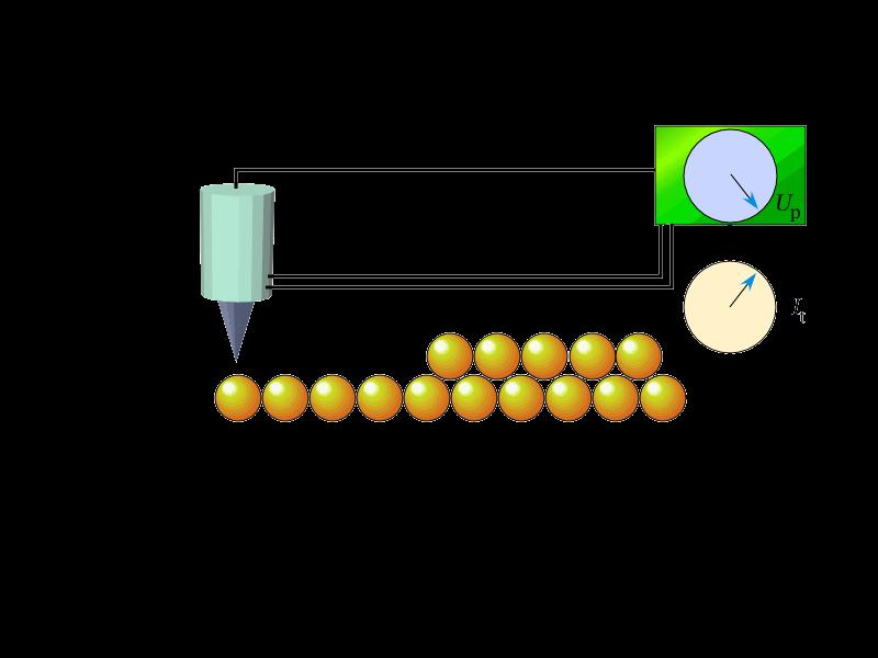
3 Scanning Tunneling Microscope: Construction Principle 1 sample 2 sample holder 3 clamps 4 tip 5 tip holder 6 scanner tube 7 approach motor rod 8 motor mount 9 approach mount 10 quartz balls 11 Zener diode 3
 enables motion in two dimensions fine-positioning of the tip: piezoelectric transducers (typically: 1 nm/v) tip specimen distance: < 1 nm (in liquids: smaller than solvent molecule")
4 Scanning Tunneling Microscope: Construction Principle design of Binnig and Rohrer (1982) vacuum (also operates in gas or liquid) atomically sharp tip piezo-electrostatic manipulator ( louse, crawls) enables motion in two dimensions fine-positioning of the tip: piezoelectric transducers (typically: 1 nm/v) tip specimen distance: < 1 nm (in liquids: smaller than solvent molecule size) 4

5 Electron Tunneling Through an Energy Barrier consider two metals separated by vacuum gap quantum mechanics: electrons can overcome energy barrier! unbiased: no net electron current tunnel barrier E F1 E b1 φ 1 φ 2 w E b2 E F2 5
 tunneling current E F1 E b1 E b2 tunneling current E F2 6")
6 Electron Tunneling Through an Energy Barrier biased (U t : net current from one metal into the other) tunneling current E F1 E b1 E b2 tunneling current E F2 6
 m 0 : electron mass; V : potential of the barrier; E: energy of the tunneling")
7 Tunneling Current solution of the stationary Schrödinger equation H = E for potential troughs separated by barrier within each trough: oscillatory wave function solution within barrier: exponential damping, [z] = [0] Exp[ z] = 1 2m 0 (V E) m 0 : electron mass; V : potential of the barrier; E: energy of the tunneling electrons; 7

8 Wave Function Across a Tunneling Barrier Separating Two Metals [z] = 0 Exp[ z] E F1 tunneling current E F2 0 z 8
![Tunneling Current as a Function of Barrier Width tunneling current at energy level E: i t [E] i t [E] is proportional to probability](/docs-images/93/113851297/images/9-1.jpg "density of finding electrons at z = w probability of finding electrons at z = w: [w] 2 therefore i t [E] [w] 2 Exp[ 2 w], = 1 2m 0 (V")
9 Tunneling Current as a Function of Barrier Width tunneling current at energy level E: i t [E] i t [E] is proportional to probability density of finding electrons at z = w probability of finding electrons at z = w: [w] 2 therefore i t [E] [w] 2 Exp[ 2 w], = 1 2m 0 (V E) 9

10 More Realistic Models for the Tunneling Current reality: image charge, image forces real specimen surface is curved results of more realistic modeling: barrier is asymmetric size and shape of the tunneling barrier depend on the barrier width w size and shape of the tunneling barrier depend on the bias voltage U t 10
 e ective work function.")
11 Tunneling Resistance Work Function magnitude of the tunneling current: a few na tunneling resistance: R t := U t /I t Fowler Nordheim relation R t [w] = Exp[Aw ] A constant with unit ev 1 nm 1 ; w width of the tunneling barrier; = 1 2 ( ) e ective work function. 11
 work function for electrons (tip and specimen) electron density electron density of states current voltage characteristics I t [U t ]")
12 Interpretation of the Measured Tunneling Current local tunneling barrier of the surface surface topography (but: maxima atoms!) work function for electrons (tip and specimen) electron density electron density of states current voltage characteristics I t [U t ] spectroscopy 12
 specimen charging electric field tunneling current distinguish real surface topography from local variations of the")
13 Problems in Practice vibrations hysteresis of piezo transducers thermal drift (di erent materials!) specimen charging electric field tunneling current distinguish real surface topography from local variations of the work function ( STS) 13
")
14 STM Modes of Operation di erent modes of STM operation provide di erent information about the specimen surface not all modes may be possible for a given specimen (surface roughness) 14
15 STM Constant-Height Mode 15
16 STM Constant-Current Mode 16

17 Topography constant-current mode operation under constant current feed-back surface topography measured quantity: voltage U z of piezoelectric transducer image: intensity height z above the surface constant-height mode high scanning speed / smooth surfaces measured quantity: tunneling current It image: intensity tunneling current 17

18 STM Resolution vertical and lateral resolution three-dimensional information atomic resolution is possible, but often STM is used with less resolution: 10 nm to 1 µm quantitative understanding: requires theory describing the tunneling current 18
19 Examples 19
 7 7")

20 STM: Si (111) 7 7 Surface Reconstruction 20

21 Example: Self-Organized Nanowires on Layered Crystals 21
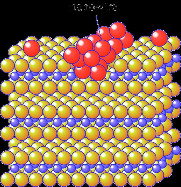
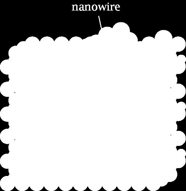
22 Example: Self-Organized Nanowires on Layered Crystals 22


23 STM: Rb Nanowires on TiTe 2 23


24 STM: Rb Nanowires on TiTe 2 24
Scanning Tunneling Microscopy
 Scanning Tunneling Microscopy The wavelike properties of electrons allows them to tunnel beyond the regions of a solid into a region of space forbidden for them to exist in. In this region they can be
A Project Report Submitted to the Faculty of the Graduate School of the University of Minnesota By
 Observation and Manipulation of Gold Clusters with Scanning Tunneling Microscopy A Project Report Submitted to the Faculty of the Graduate School of the University of Minnesota By Dogukan Deniz In Partial
Unit-25 Scanning Tunneling Microscope (STM)
") Unit-5 Scanning Tunneling Microscope (STM) Objective: Imaging formation of scanning tunneling microscope (STM) is due to tunneling effect of quantum physics, which is in nano scale. This experiment shows
Unit-5 Scanning Tunneling Microscope (STM) Objective: Imaging formation of scanning tunneling microscope (STM) is due to tunneling effect of quantum physics, which is in nano scale. This experiment shows
; A=4π(2m) 1/2 /h. exp (Fowler Nordheim Eq.) 2 const
 1/2 /h. exp (Fowler Nordheim Eq.) 2 const") Scanning Tunneling Microscopy (STM) Brief background: In 1981, G. Binnig, H. Rohrer, Ch. Gerber and J. Weibel observed vacuum tunneling of electrons between a sharp tip and a platinum surface. The tunnel
Scanning Tunneling Microscopy (STM) Brief background: In 1981, G. Binnig, H. Rohrer, Ch. Gerber and J. Weibel observed vacuum tunneling of electrons between a sharp tip and a platinum surface. The tunnel
CONSTRUCTING A SCANNING TUNNELING MICROSCOPE FOR THE STUDY OF SUPERCONDUCTIVITY
 CONSTRUCTING A SCANNING TUNNELING MICROSCOPE FOR THE STUDY OF SUPERCONDUCTIVITY CHRISTOPHER STEINER 2012 NSF/REU Program Physics Department, University of Notre Dame Advisors: DR. MORTEN ESKILDSEN CORNELIUS
Advanced Nanoscale Metrology with AFM
 Advanced Nanoscale Metrology with AFM Sang-il Park Corp. SPM: the Key to the Nano World Initiated by the invention of STM in 1982. By G. Binnig, H. Rohrer, Ch. Gerber at IBM Zürich. Expanded by the invention
Outline: Introduction: What is SPM, history STM AFM Image treatment Advanced SPM techniques Applications in semiconductor research and industry
 1 Outline: Introduction: What is SPM, history STM AFM Image treatment Advanced SPM techniques Applications in semiconductor research and industry 2 Back to our solutions: The main problem: How to get nm
Controller Design for Z Axis Movement of STM Using SPM Control Software
 Controller Design for Z Axis Movement of STM Using SPM Control Software Neena Tom, Rini Jones S. B Abstract Scanning probe microscopy is a branch of microscopy that forms images of surfaces using a physical
Nanovie. Scanning Tunnelling Microscope
 Nanovie Scanning Tunnelling Microscope Nanovie STM Always at Hand Nanovie STM Lepto for Research Nanovie STM Educa for Education Nanovie Auto Tip Maker Nanovie STM Lepto Portable 3D nanoscale microscope
Radio-frequency scanning tunneling microscopy
 doi: 10.1038/nature06238 SUPPLEMENARY INFORMAION Radio-frequency scanning tunneling microscopy U. Kemiktarak 1,. Ndukum 2, K.C. Schwab 2, K.L. Ekinci 3 1 Department of Physics, Boston University, Boston,
LOW TEMPERATURE STM/AFM
 * CreaTec STM of Au(111) using a CO-terminated tip, 20mV bias, 0.6nA* LOW TEMPERATURE STM/AFM High end atomic imaging, spectroscopy and manipulation Designed and manufactured in Germany by CreaTec Fischer
Atomic Force Microscopy (Bruker MultiMode Nanoscope IIIA)
") Atomic Force Microscopy (Bruker MultiMode Nanoscope IIIA) This operating procedure intends to provide guidance for general measurements with the AFM. For more advanced measurements or measurements with
Atomic Force Microscopy (Bruker MultiMode Nanoscope IIIA) This operating procedure intends to provide guidance for general measurements with the AFM. For more advanced measurements or measurements with
Design and Construction of a Variable Temperature Atomic Force Microscope. Bethany J. Little
 Design and Construction of a Variable Temperature Atomic Force Microscope By Bethany J. Little A thesis submitted in partial fulfillment of the requirements for the degree of Bachelor of Science Houghton
Supporting Information. Atomic-scale Spectroscopy of Gated Monolayer MoS 2
 Height (nm) Supporting Information Atomic-scale Spectroscopy of Gated Monolayer MoS 2 Xiaodong Zhou 1, Kibum Kang 2, Saien Xie 2, Ali Dadgar 1, Nicholas R. Monahan 3, X.-Y. Zhu 3, Jiwoong Park 2, and Abhay
Atomic resolution of the graphite surface by STM
 Related Topics Tunneling effect, Hexagonal Structures, Scanning Tunneling Microscopy (STM), Imaging on the subnanometer scale, Piezo-electric devices, Local Density of States (LDOS), Constant-Height and
Measurement of Microscopic Three-dimensional Profiles with High Accuracy and Simple Operation
 238 Hitachi Review Vol. 65 (2016), No. 7 Featured Articles Measurement of Microscopic Three-dimensional Profiles with High Accuracy and Simple Operation AFM5500M Scanning Probe Microscope Satoshi Hasumura
Lecture 20: Optical Tools for MEMS Imaging
 MECH 466 Microelectromechanical Systems University of Victoria Dept. of Mechanical Engineering Lecture 20: Optical Tools for MEMS Imaging 1 Overview Optical Microscopes Video Microscopes Scanning Electron
Contents 1 Introduction 3 2 What is STM? 3 3 Scanning with 'easyscan' 4 4 Experiments Tip Preparation and Installation
 'easyscan' SCANNING TUNNELING MICROSCOPE Baris Cetin Department of Physics Purdue University, West Lafayette, In 47907 Abstract A summary of the fundemental principals in using a 'easyscan' STM "Scanning
Proposal. Design of a Scanning Tunneling Microscope
 Proposal Design of a Scanning Tunneling Microscope Submitted to The Engineering Honors Committee 119 Hitchcock Hall College of Engineering The Ohio State University Columbus, Ohio 43210 Abstract This proposal
- Near Field Scanning Optical Microscopy - Electrostatic Force Microscopy - Magnetic Force Microscopy
 - Near Field Scanning Optical Microscopy - Electrostatic Force Microscopy - Magnetic Force Microscopy Yongho Seo Near-field Photonics Group Leader Wonho Jhe Director School of Physics and Center for Near-field
2. Operating modes in scanning probe microscopy
 . Operating modes in scanning probe microscopy.1. Scanning tunneling microscopy Historically, the first microscope in the family of probe microscopes is the scanning tunneling microscope. The working principle
Park NX-Hivac: Phase-lock Loop for Frequency Modulation Non-Contact AFM
 Park Atomic Force Microscopy Application note #21 www.parkafm.com Hosung Seo, Dan Goo and Gordon Jung, Park Systems Corporation Romain Stomp and James Wei Zurich Instruments Park NX-Hivac: Phase-lock Loop
NanoFocus Inc. Next Generation Scanning Probe Technology. Tel : Fax:
 NanoFocus Inc. Next Generation Scanning Probe Technology www.nanofocus.kr Tel : 82-2-864-3955 Fax: 82-2-864-3956 Albatross SPM is Multi functional research grade system Flexure scanner and closed-loop
Exam Signal Detection and Noise
 Exam Signal Detection and Noise Tuesday 27 January 2015 from 14:00 until 17:00 Lecturer: Sense Jan van der Molen Important: It is not allowed to use a calculator. Complete each question on a separate piece
Intrinsic Semiconductor
 Semiconductors Crystalline solid materials whose resistivities are values between those of conductors and insulators. Good electrical characteristics and feasible fabrication technology are some reasons
Imaging Carbon Nanotubes Magdalena Preciado López, David Zahora, Monica Plisch
 Imaging Carbon Nanotubes Magdalena Preciado López, David Zahora, Monica Plisch I. Introduction In this lab you will image your carbon nanotube sample from last week with an atomic force microscope. You
Cutting-edge Atomic Force Microscopy techniques for large and multiple samples
 Cutting-edge Atomic Force Microscopy techniques for large and multiple samples Study of up to 200 mm samples using the widest set of AFM modes Industrial standards of automation A unique combination of
Park NX20 The leading nano metrology tool for failure analysis and large sample research.
 The Most Accurate Atomic Force Microscope Park NX20 The leading nano metrology tool for failure analysis and large sample research www.parkafm.com The Most Accurate Atomic Force Microscope Park NX20 The
Prepare Sample 3.1. Place Sample in Stage. Replace Probe (optional) Align Laser 3.2. Probe Approach 3.3. Optimize Feedback 3.4. Scan Sample 3.
 Align Laser 3.2. Probe Approach 3.3. Optimize Feedback 3.4. Scan Sample 3.") CHAPTER 3 Measuring AFM Images Learning to operate an AFM well enough to get an image usually takes a few hours of instruction and practice. It takes 5 to 10 minutes to measure an image if the sample is
CHAPTER 3 Measuring AFM Images Learning to operate an AFM well enough to get an image usually takes a few hours of instruction and practice. It takes 5 to 10 minutes to measure an image if the sample is
Manufacturing Metrology Team
 The Team has a range of state-of-the-art equipment for the measurement of surface texture and form. We are happy to discuss potential measurement issues and collaborative research Manufacturing Metrology
MEMS for RF, Micro Optics and Scanning Probe Nanotechnology Applications
 MEMS for RF, Micro Optics and Scanning Probe Nanotechnology Applications Part I: RF Applications Introductions and Motivations What are RF MEMS? Example Devices RFIC RFIC consists of Active components
Study of shear force as a distance regulation mechanism for scanning near-field optical microscopy
 Study of shear force as a distance regulation mechanism for scanning near-field optical microscopy C. Durkan a) and I. V. Shvets Department of Physics, Trinity College Dublin, Ireland Received 31 May 1995;
Self-navigation of STM tip toward a micron sized sample
 Self-navigation of STM tip toward a micron sized sample Guohong Li, Adina Luican, and Eva Y. Andrei Department of Physics & Astronomy, Rutgers University, Piscataway, New Jersey 08854, USA We demonstrate
SENSOR+TEST Conference SENSOR 2009 Proceedings II
 B8.4 Optical 3D Measurement of Micro Structures Ettemeyer, Andreas; Marxer, Michael; Keferstein, Claus NTB Interstaatliche Hochschule für Technik Buchs Werdenbergstr. 4, 8471 Buchs, Switzerland Introduction
ATOMIC FORCE MICROSCOPY
 B47 Physikalisches Praktikum für Fortgeschrittene Supervision: Prof. Dr. Sabine Maier sabine.maier@physik.uni-erlangen.de ATOMIC FORCE MICROSCOPY Version: E1.4 first edit: 15/09/2015 last edit: 05/10/2018
The Most Accurate Atomic Force Microscope. Park NX20 The leading nano metrology tool for failure analysis and large sample research.
 The Most Accurate Atomic Force Microscope Park NX20 The leading nano metrology tool for failure analysis and large sample research www.parkafm.com Park Systems The Most Accurate Atomic Force Microscope
Virtual Scanning Tunneling Microscope Offered as a Free-Download
 Mark Hagmann*, Greg Spencer, and Jeremy Wiedemeier NewPath Research L.L.C., 2880 S. Main St., Ste. 214, Salt Lake City, UT 84115 *newpathresearch@gmail.com Abstract: The scanning tunneling microscope is
Vibration Isolation for Scanning Tunneling Microscopy
 Vibration Isolation for Scanning Tunneling Microscopy Catherine T. Truett Department of Physics, Michigan State University East Lansing, Michigan 48824 ABSTRACT Scanning Tunneling Microscopy measures tunneling
State of the Art Room Temperature Scanning Hall Probe Microscopy using High Performance micro-hall Probes
 State of the Art Room Temperature Scanning Hall Probe Microscopy using High Performance micro-hall Probes A. Sandhu 1, 4, H. Masuda 2, A. Yamada 1, M. Konagai 3, A. Oral 5, S.J Bending 6 RCQEE, Tokyo Inst.
Lund University Faculty of Science. STM-based characterization of single GaInP photovoltaic nanowires
 Lund University Faculty of Science STM-based characterization of single GaInP photovoltaic nanowires Author: Johannes Brask Supervisor: Rainer Timm Co-supervisor: Magnus Borgström Bachelor thesis Div.
BioInstrumentation Laboratory
 BioInstrumentation Laboratory Ian Hunter Vienna, May 22 2013 BioInstrumentation Lab, Mechanical Engineering, MIT - Robotic endoscopes - Needle-free drug delivery devices - Eye micro-surgery robots - High
Operating Instructions. easyscan E-STM Version 2.0
 Operating Instructions easyscan E-STM Version 2.0 1 TEXT & LAYOUT: KARIN HOOL, R. SUM, PIETER VAN SCHENDEL ENGLISH: VICKY CONNOLLY NANOSURF AND THE NANOSURF LOGO ARE TRADEMARKS OF NANOSURF AG, REGISTERED
INTRODUCTION. Have applications for imaging, detection and navigation.
 ULTRASONICS INTRODUCTION The word ultrasonic combines the Latin roots ultra - beyond sonic - sound. Having frequencies above the audible range i.e. above 20000Hz Have applications for imaging, detection
Ch5 Diodes and Diodes Circuits
 Circuits and Analog Electronics Ch5 Diodes and Diodes Circuits 5.1 The Physical Principles of Semiconductor 5.2 Diodes 5.3 Diode Circuits 5.4 Zener Diode References: Floyd-Ch2; Gao-Ch6; 5.1 The Physical
Oxford Scholarship Online
 University Press Scholarship Online Oxford Scholarship Online Atomic Force Microscopy Peter Eaton and Paul West Print publication date: 2010 Print ISBN-13: 9780199570454 Published to Oxford Scholarship
10/27/2009 Reading: Chapter 10 of Hambley Basic Device Physics Handout (optional)
") EE40 Lec 17 PN Junctions Prof. Nathan Cheung 10/27/2009 Reading: Chapter 10 of Hambley Basic Device Physics Handout (optional) Slide 1 PN Junctions Semiconductor Physics of pn junctions (for reference
EE40 Lec 17 PN Junctions Prof. Nathan Cheung 10/27/2009 Reading: Chapter 10 of Hambley Basic Device Physics Handout (optional) Slide 1 PN Junctions Semiconductor Physics of pn junctions (for reference
Tip-induced band bending and its effect on local barrier height measurement studied by light-modulated scanning tunneling spectroscopy
 e-journal of Surface Science and Nanotechnology 10 February 2006 e-j. Surf. Sci. Nanotech. Vol. 4 (2006) 192-196 Conference - ISSS-4 - Tip-induced band bending and its effect on local barrier height measurement
SUPPLEMENTARY INFORMATION
 SUPPLEMENTARY INFORMATION Supplementary Information Real-space imaging of transient carrier dynamics by nanoscale pump-probe microscopy Yasuhiko Terada, Shoji Yoshida, Osamu Takeuchi, and Hidemi Shigekawa*
WAVES. Chapter Fifteen MCQ I
 Chapter Fifteen WAVES MCQ I 15.1 Water waves produced by a motor boat sailing in water are (a) neither longitudinal nor transverse. (b) both longitudinal and transverse. (c) only longitudinal. (d) only
Scanning electron microscope
 Scanning electron microscope 5 th CEMM workshop Maja Koblar, Sc. Eng. Physics Outline The basic principle? What is an electron? Parts of the SEM Electron gun Electromagnetic lenses Apertures Detectors
Review Energy Bands Carrier Density & Mobility Carrier Transport Generation and Recombination
 Review Energy Bands Carrier Density & Mobility Carrier Transport Generation and Recombination Current Transport: Diffusion, Thermionic Emission & Tunneling For Diffusion current, the depletion layer is
Atomic Scale Patterning Made Easy
 ZyVector STM Control System for Atomically Precise Lithography Making Atomic Resolution Lithography a reality Distributed by Distortion-Free Imaging Automatic Lattice Alignment Digital Vector Lithography
p q p f f f q f p q f NANO 703-Notes Chapter 5-Magnification and Electron Sources
 Chapter 5-agnification and Electron Sources Lens equation Let s first consider the properties of an ideal lens. We want rays diverging from a point on an object in front of the lens to converge to a corresponding
Surface Modification in Air with a Scanning Tunneling Microscope Developed In-House
 Surface Modification in Air with a Scanning Tunneling Microscope Developed In-House by Jason Yongjun Pahng Submitted to the Department of Mechanical Engineering in partial fulfillment of the requirements
Supporting Information. Vertical Graphene-Base Hot-Electron Transistor
 Supporting Information Vertical Graphene-Base Hot-Electron Transistor Caifu Zeng, Emil B. Song, Minsheng Wang, Sejoon Lee, Carlos M. Torres Jr., Jianshi Tang, Bruce H. Weiller, and Kang L. Wang Department
Lateral Force: F L = k L * x
 Scanning Force Microscopy (SFM): Conventional SFM Application: Topography measurements Force: F N = k N * k N Ppring constant: Spring deflection: Pieo Scanner Interaction or force dampening field Contact
SECONDARY ELECTRON DETECTION
 SECONDARY ELECTRON DETECTION CAMTEC Workshop Presentation Haitian Xu June 14 th 2010 Introduction SEM Raster scan specimen surface with focused high energy e- beam Signal produced by beam interaction with
Diode conducts when V anode > V cathode. Positive current flow. Diodes (and transistors) are non-linear device: V IR!
 are non-linear device: V IR!") Diodes: What do we use diodes for? Lecture 5: Diodes and Transistors protect circuits by limiting the voltage (clipping and clamping) turn AC into DC (voltage rectifier) voltage multipliers (e.g. double
Diodes: What do we use diodes for? Lecture 5: Diodes and Transistors protect circuits by limiting the voltage (clipping and clamping) turn AC into DC (voltage rectifier) voltage multipliers (e.g. double
University of Nevada, Reno
 University of Nevada, Reno Design and Characterization of Scanning Probe Microscopy Platform with Active Electro-Thermal Microcantilever for Multifunctional Applications A thesis submitted in partial fulfillment
Electronics The basics of semiconductor physics
 Electronics The basics of semiconductor physics Prof. Márta Rencz, Gábor Takács BME DED 17/09/2015 1 / 37 The basic properties of semiconductors Range of conductivity [Source: http://www.britannica.com]
attocfm I for Surface Quality Inspection NANOSCOPY APPLICATION NOTE M01 RELATED PRODUCTS G
 APPLICATION NOTE M01 attocfm I for Surface Quality Inspection Confocal microscopes work by scanning a tiny light spot on a sample and by measuring the scattered light in the illuminated volume. First,
1. Introduction. 2. Concept. reflector. transduce r. node. Kraftmessung an verschiedenen Fluiden in akustischen Feldern
 1. Introduction The aim of this Praktikum is to familiarize with the concept and the equipment of acoustic levitation and to measure the forces exerted by an acoustic field on small spherical objects.
Near-field Optical Microscopy
 Near-field Optical Microscopy R. Fernandez, X. Wang, N. Li, K. Parker, and A. La Rosa Physics Department Portland State University Portland, Oregon Near-Field SPIE Optics Microscopy East 2005 Group PSU
Reg. No. : Question Paper Code : B.E./B.Tech. DEGREE EXAMINATION, NOVEMBER/DECEMBER Second Semester
 WK 5 Reg. No. : Question Paper Code : 27184 B.E./B.Tech. DEGREE EXAMINATION, NOVEMBER/DECEMBER 2015. Time : Three hours Second Semester Electronics and Communication Engineering EC 6201 ELECTRONIC DEVICES
DESIGN OF FEEDBACK CIRCUIT OF SCANNING TUNNELING MICROSCOPE USING CURRENT CONVEYOR
 Journal of Electron Devices, Vol. 13, 212, pp. 997-11 JED [ISSN: 1682-3427 ] DESIGN OF FEEDBACK CIRCUIT OF SCANNING TUNNELING MICROSCOPE USING CURRENT CONVEYOR Sajal K. Paul, Mourina Ghosh, Ashish Ranjan
University of Alberta. Library Release Form. Title of Thesis: Junction Mixing Scanning Tunneling Microscopy
 University of Alberta Library Release Form Name of Author: Geoffrey Mark Steeves Title of Thesis: Junction Mixing Scanning Tunneling Microscopy Degree: Doctor of Philosophy Year this Degree Granted: 2001
Realization of H.O.: Lumped Element Resonator
 Realization of H.O.: Lumped Element Resonator inductor L capacitor C a harmonic oscillator currents and magnetic fields +q -q charges and electric fields Realization of H.O.: Transmission Line Resonator
semiconductor p-n junction Potential difference across the depletion region is called the built-in potential barrier, or built-in voltage:
 Chapter four The Equilibrium pn Junction The Electric field will create a force that will stop the diffusion of carriers reaches thermal equilibrium condition Potential difference across the depletion
Akiyama-Probe (A-Probe) guide
 guide") Akiyama-Probe (A-Probe) guide This guide presents: what is Akiyama-Probe, how it works, and what you can do Dynamic mode AFM Version: 2.0 Introduction NANOSENSORS Akiyama-Probe (A-Probe) is a self-sensing
Akiyama-Probe (A-Probe) guide This guide presents: what is Akiyama-Probe, how it works, and what you can do Dynamic mode AFM Version: 2.0 Introduction NANOSENSORS Akiyama-Probe (A-Probe) is a self-sensing
Atomic Force Microscopy (I)
") Atomic Force Microscopy (I) - Optical Grating AFM and the thermal noise measurement 2.674 Lab 10 Spring 2016 Pappalardo II Micro/Nano Laboratories AFM Imaging (with home-made AFMs) I. Safety Notes This
Atomic Force Microscopy (I) - Optical Grating AFM and the thermal noise measurement 2.674 Lab 10 Spring 2016 Pappalardo II Micro/Nano Laboratories AFM Imaging (with home-made AFMs) I. Safety Notes This
Measurement Techniques
 Measurement Techniques Anders Sjöström Juan Negreira Montero Department of Construction Sciences. Division of Engineering Acoustics. Lund University Disposition Introduction Errors in Measurements Signals
High Resolution Imaging of Nanoscale Structures by Scanning Probe Microscopy Techniques
 High Resolution Imaging of Nanoscale Structures by Scanning Probe Microscopy Techniques Prof. Marco Farina, Senior Member IEEE Dipartimento di Ingegneria dell Informazione Università Politecnica delle
EDC Lecture Notes UNIT-1
 P-N Junction Diode EDC Lecture Notes Diode: A pure silicon crystal or germanium crystal is known as an intrinsic semiconductor. There are not enough free electrons and holes in an intrinsic semi-conductor
Alejandro Mendez, Ph.D. President & CEO Mendezized Metals Corporation
 ATOMIC FORCE MICROSCOPY (AFM) PHOTO CONDUCTIVE ANALYSIS AND CALCULATION FOR REGULAR AND MENDEZIZED COMMERCIAL 24 KARATS GOLD BARS CONDUCTED IN FIVE DIFFERENT TRIPLICATE SERIES. Date: June 23, 2016 Conducted
Microscopic Basis for the Mechanism of Carrier Dynamics in an Operating p-n Junction Examined by using Light-Modulated Scanning Tunneling Spectroscopy
 Microscopic Basis for the Mechanism of Carrier Dynamics in an Operating p-n Junction Examined by using Light-Modulated Scanning Tunneling Spectroscopy Shoji Yoshida, Yuya Kanitani, Ryuji Oshima, Yoshitaka
Basic methods in imaging of micro and nano structures with atomic force microscopy (AFM)
") Basic methods in imaging of micro and nano P2538000 AFM Theory The basic principle of AFM is very simple. The AFM detects the force interaction between a sample and a very tiny tip (
Basic methods in imaging of micro and nano P2538000 AFM Theory The basic principle of AFM is very simple. The AFM detects the force interaction between a sample and a very tiny tip (
attosnom I: Topography and Force Images NANOSCOPY APPLICATION NOTE M06 RELATED PRODUCTS G
 APPLICATION NOTE M06 attosnom I: Topography and Force Images Scanning near-field optical microscopy is the outstanding technique to simultaneously measure the topography and the optical contrast of a sample.
Lecture 18: Photodetectors
 Lecture 18: Photodetectors Contents 1 Introduction 1 2 Photodetector principle 2 3 Photoconductor 4 4 Photodiodes 6 4.1 Heterojunction photodiode.................... 8 4.2 Metal-semiconductor photodiode................
Microscopy. ( greek mikros = small; skopein = to observe)
") Microscopy ( greek mikros = small; skopein = to observe) Zacharias Jansen put several lenses in a tube (first compound microscope) and the object near the end of tube appeared to be greatly enlarged, much
Microscopy ( greek mikros = small; skopein = to observe) Zacharias Jansen put several lenses in a tube (first compound microscope) and the object near the end of tube appeared to be greatly enlarged, much
PSD Characteristics. Position Sensing Detectors
 PSD Characteristics Position Sensing Detectors Silicon photodetectors are commonly used for light power measurements in a wide range of applications such as bar-code readers, laser printers, medical imaging,
Nanomechanical Mapping of a High Curvature Polymer Brush Grafted
 Supplementary Information Nanomechanical Mapping of a High Curvature Polymer Brush Grafted from a Rigid Nanoparticle Gunnar Dunér 1, Esben Thormann 1, Andra Dėdinaitė 1,2, Per M. Claesson 1,2, Krzysztof
INDIAN INSTITUTE OF TECHNOLOGY BOMBAY
 IIT Bombay requests quotations for a high frequency conducting-atomic Force Microscope (c-afm) instrument to be set up as a Central Facility for a wide range of experimental requirements. The instrument
Active mechanical noise cancellation scanning tunneling microscope
 REVIEW OF SCIENTIFIC INSTRUMENTS 78, 073705 2007 Active mechanical noise cancellation scanning tunneling microscope H. Liu, Y. Meng, H. W. Zhao, and D. M. Chen a Beijing National Laboratory for Condensed
Exploring the Electron Tunneling Behavior of Scanning Tunneling Microscope (STM) tip and n-type Semiconductor
 tip and n-type Semiconductor") Page 110 Exploring the of Scanning Tunneling Microscope (STM) tip and n-type Seiconductor M. A. Rahan * and J. U. Ahed Departent of Applied Physics, Electronics & Counication Engineering, University of
Page 110 Exploring the of Scanning Tunneling Microscope (STM) tip and n-type Seiconductor M. A. Rahan * and J. U. Ahed Departent of Applied Physics, Electronics & Counication Engineering, University of
Physics 160 Lecture 5. R. Johnson April 13, 2015
 Physics 160 Lecture 5 R. Johnson April 13, 2015 Half Wave Diode Rectifiers Full Wave April 13, 2015 Physics 160 2 Note that there is no ground connection on this side of the rectifier! Output Smoothing
EXPERIMENT 12 PHYSICS 250 TRANSDUCERS: TIME RESPONSE
 EXPERIMENT 12 PHYSICS 250 TRANSDUCERS: TIME RESPONSE Apparatus: Signal generator Oscilloscope Digital multimeter Microphone Photocell Hall Probe Force transducer Force generator Speaker Light sources Calibration
KOM2751 Analog Electronics :: Dr. Muharrem Mercimek :: YTU - Control and Automation Dept. 1 1 (CONT D) DIODES
 DIODES") KOM2751 Analog Electronics :: Dr. Muharrem Mercimek :: YTU - Control and Automation Dept. 1 1 (CONT D) DIODES Most of the content is from the textbook: Electronic devices and circuit theory, Robert L.
KOM2751 Analog Electronics :: Dr. Muharrem Mercimek :: YTU - Control and Automation Dept. 1 1 (CONT D) DIODES Most of the content is from the textbook: Electronic devices and circuit theory, Robert L.
Akiyama-Probe (A-Probe) guide
 guide") Akiyama-Probe (A-Probe) guide This guide presents: what is Akiyama-Probe, how it works, and its performance. Akiyama-Probe is a patented technology. Version: 2009-03-23 Introduction NANOSENSORS Akiyama-Probe
Akiyama-Probe (A-Probe) guide This guide presents: what is Akiyama-Probe, how it works, and its performance. Akiyama-Probe is a patented technology. Version: 2009-03-23 Introduction NANOSENSORS Akiyama-Probe
Optical Microscope. Active anti-vibration table. Mechanical Head. Computer and Software. Acoustic/Electrical Shield Enclosure
 Optical Microscope On-axis optical view with max. X magnification Motorized zoom and focus Max Field of view: mm x mm (depends on zoom) Resolution : um Working Distance : mm Magnification : max. X Zoom
 Electronic Devices 1. Current flowing in each of the following circuits A and respectively are: (Circuit 1) (Circuit 2) 1) 1A, 2A 2) 2A, 1A 3) 4A, 2A 4) 2A, 4A 2. Among the following one statement is not
Physics 623 Transistor Characteristics and Single Transistor Amplifier Sept. 12, 2017
 Physics 623 Transistor Characteristics and Single Transistor Amplifier Sept. 12, 2017 1 Purpose To measure and understand the common emitter transistor characteristic curves. To use the base current gain
Medical Imaging. X-rays, CT/CAT scans, Ultrasound, Magnetic Resonance Imaging
 Medical Imaging X-rays, CT/CAT scans, Ultrasound, Magnetic Resonance Imaging From: Physics for the IB Diploma Coursebook 6th Edition by Tsokos, Hoeben and Headlee And Higher Level Physics 2 nd Edition
RECENTLY, using near-field scanning optical
 1 2 1 2 Theoretical and Experimental Study of Near-Field Beam Properties of High Power Laser Diodes W. D. Herzog, G. Ulu, B. B. Goldberg, and G. H. Vander Rhodes, M. S. Ünlü L. Brovelli, C. Harder Abstract
Electronic devices-i. Difference between conductors, insulators and semiconductors
 Electronic devices-i Semiconductor Devices is one of the important and easy units in class XII CBSE Physics syllabus. It is easy to understand and learn. Generally the questions asked are simple. The unit
Transport properties of InAs Nanowhiskers
 Transport properties of InAs Nanowhiskers Master Thesis to obtain the degree of Master of Science Physics at Fachbereich Physik Universität Duisburg-Essen submitted by Vadim Migunov from Sarov, Russian
Tunneling transport of mono- and few-layers magnetic van der Waals MnPS3
 Tunneling transport of mono- and few-layers magnetic van der Waals MnPS3 Sungmin Lee, 1,2 Ki-Young Choi, 1 Sangik Lee, 3 Bae Ho Park, 3 and Je-Geun Park 1,2,a) 1 Center for Correlated Electron Systems,
Q-Motion Miniature Linear Stage
 Q-Motion Miniature Stage Smallest linear stage with position control, high resolution and affordable price Q-521 Only 21 mm wide and 10 mm high Direct position measurement with integrated incremental,
5. Transducers Definition and General Concept of Transducer Classification of Transducers
 5.1. Definition and General Concept of Definition The transducer is a device which converts one form of energy into another form. Examples: Mechanical transducer and Electrical transducer Electrical A
Lecture 7:PN Junction. Structure, Depletion region, Different bias Conditions, IV characteristics, Examples
 Lecture 7:PN Junction Structure, Depletion region, Different bias Conditions, IV characteristics, Examples PN Junction The diode (pn junction) is formed by dopping a piece of intrinsic silicon, such that
CHAPTER 8 The PN Junction Diode
 CHAPTER 8 The PN Junction Diode Consider the process by which the potential barrier of a PN junction is lowered when a forward bias voltage is applied, so holes and electrons can flow across the junction