POLYMER MICROSTRUCTURE WITH TILTED MICROPILLAR ARRAY AND METHOD OF FABRICATING THE SAME
|
|
|
- Margaret Simon
- 5 years ago
- Views:
Transcription
1 POLYMER MICROSTRUCTURE WITH TILTED MICROPILLAR ARRAY AND METHOD OF FABRICATING THE SAME Field of the Invention The present invention relates to a polymer microstructure. In particular, the present invention relates to a polymer microstructure with a tilted micropillar array formed by adjusting an incident angle for ion beam treatment, and a method of fabricating the same. Background of the Invention As well known in the art, there have been studies on 1 the life in the natural world and natural phenomenon. In recent years, there are observations of hydrophobicity on pure water where a lotus blossom, a lizard, a water strider, or the like appears, and there are active studies on the structures concerned. That is, a lizard or insect goes up and down the wall or slope, or a water strider walks on the water, so the sole structure of the lizard, insect, or water strider is attracting intention. The existing studies have found that a lizard, an insect, or a water strider has a multilayer 2 ciliated sole structure, and this structure has a hydrophobic property and sufficient adhesion to the wall. -1-
2 In this structure, it is important to structurally control the adhesion strength such that a lizard or insect can walk the wall or ceiling without falling. That is, the ciliated sole structure of the insect or lizard arbitrarily is configured such that adhesion is maintained or weakened as occasion demands. In particular, there are many studies on the ciliated sole structure of the lizard. The existing studies have evaluated adhesion between linear micropillar structures and the surface, on which the micropillar structures are supported. In the ciliated sole structure of the lizard, the cilla are tilted in a predetermined direction, not linear, so it is necessary to form a nanostructure with an asymmetric tilted structure. In recent years, as described 1 in S. Reddy et al, Advanced Materials 19(07) , linear pillars are tilted by using a shape memory polymer material. In this case, however, a polymer is a hard shape memory polymer, so the polymer is only bent by a relatively small amount. As a result, it is difficult to form a nanostructure with an asymmetric tilted structure. Summary of the Invention In view of the above, the invention provides a polymer 2 microstructure with a tilted micropillar array is formed, and a method of fabricating the same. -2-
3 An aspect of the invention provides a polymer microstructure with a tilted micropillar array. The polymer microstructure is made of a soft polymer material with a micropillar array. The tilted micropillar array is formed by either thin film coating or sputtering of a metal/nonmetal material while adjusting an incident angle for ion beam treatment over the entire top surface of the micropillar array. Another aspect of the invention provides a method of fabricating a polymer microstructure with a tilted micropillar array. The method includes the steps of forming a soft polymer sample with a linear micropillar array, fixing the soft polymer sample onto a jig having a predetermined tilt angle within a chamber, and performing 1 ion beam treatment on the top surface of the linear micropillar array so as to form the tilted micropillar array. According to the aspects of the invention, the tilted micropillar array is formed by adjusting the incident angle for ion beam treatment, so the present invention can be applied in fabricating an adhesive material with dry selfcleaning, a micro robot which can goes up the wall, a wafer aligner for a semiconductor manufacturing line, and the like. According to the aspects of the present invention, the tilted micropillar array can be formed on the surface of the 2 polymer by the ion beam treatment where a plasma ionization rate is increased by the PECVD (Plasma-Enhanced Chemical -3-
4 Vapor Deposition) method with low energy consumption. Further, the micropillars can be tilted at a desired angle by adjusting at least one of the incident angle, the irradiation time, and the magnitude of acceleration voltage of the ion beam for the ion beam treatment. According to the aspects of the present invention, with the lithography method, the low vacuum condition, and the low bias voltage condition, the substrate can be prevented from being damaged. Brief Description of the Drawings The above and other features of the present invention will become apparent from the following description of an 1 embodiment given in conjunction with the accompanying drawings, in which: Fig. 1A is a schematic view of ion beam treatment on an upright micropillar array of a polymer microstructure according to an embodiment of the invention; Fig. 1B shows an SEM image of the surface of a tilted micropillar array according to the embodiment of the invention; Fig. 2A is a schematic view of a hybrid ion beam deposition apparatus for ion beam treatment on a micropillar 2 array according to the embodiment of the invention; Fig. 2B is a diagram showing the shape of a jig -4-
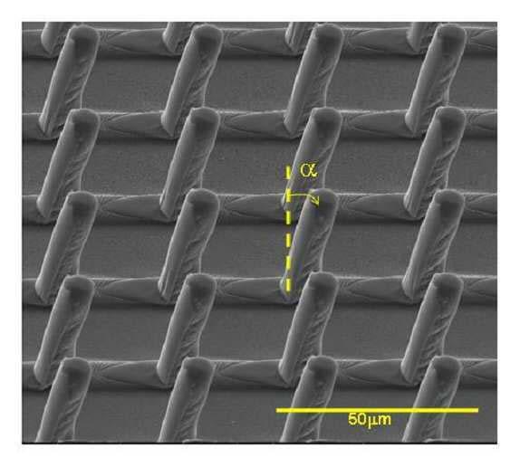
5 disposed within a hybrid ion beam deposition apparatus and the surface of PDMS, which is a polymer material with a micropillar array, placed at a predetermined tilt angle (α) on the jig according to the embodiment of the invention; Figs. 3A and 3C show SEM images of an upright linear micropillar array; Figs. 3B and 3D show SEM images of a micropillar array tilted in one direction; Fig. 4A shows an SEM image of a linear micropillar array before ion beam treatment is performed; Fig. 4B shows an SEM image of a tilted micropillar array, which is formed with an incident angle for ion beam treatment tilted at α=, according to the embodiment of the invention; 1 Fig. 4C shows an SEM image of a tilted micropillar array, which is formed with an incident angle for ion beam treatment tilted at α=40, according to the embodiment of the invention; Figs. A and B show SEM images where wrinkles are observed in a portion, in which no micropillar array is formed, due to a change in voltage according to the embodiment of the invention; Fig. C is a graph showing a wrinkle wavelength according to the embodiment of the invention; 2 Fig. 6A is a graph showing a change in wavelength to an irradiation time when a bias voltage is constant at
6 V, according to the embodiment of the invention; Fig. 6B is a graph showing a change in amplitude to an irradiation time according to the embodiment of the invention; Fig. 7A is a graph showing a tilt angle of a micropillar to an angle between a micropillar array and an ion beam for ion beam treatment according to the embodiment of the invention; Fig. 7B shows an SEM image of a micropillar tilted at α=40 according to the embodiment of the invention; and Fig. 7C shows an SEM image of a micropillar tilted at α=80 according to the embodiment of the invention. Detailed Description of the Embodiments 1 The operation principle of the invention will now be described in detail with reference to the accompanying drawings. In the following description, detailed description of known functions and structures incorporated herein will be omitted when it may make the subject matter of the present invention unclear. Fig. 1A is a schematic view of ion beam treatment on an upright micropillar array of a polymer microstructure according to an embodiment of the present invention. Fig. 2 1B shows an SEM (Scanning Electron Microscopy) image of the surface of a tilted micropillar array according to the -6-
7 embodiment of the present invention. Referring to Figs. 1A and 1B, an array of linear micropillars (for example, one of pillar, dots, holes, and walls having a convex shape) is formed on the surface of PDMS 1, which is a soft polymer material, under the high vacuum condition, and ion beams 3 are obliquely irradiated from an ion beam deposition apparatus onto the entire top surface of the micropillar array by any one of PECVD, PSII (plasma source ion implantation), filtered vacuum arc, atmospheric plasma treatment method and ion beam method. Thus, the micropillar array on the surface of the PDMS 1 is changed into a tilted micropillar array. The incident angle is an angle between the acceleration direction of the ion beams and the polymer 1 material. The dedicated ion beam, one of argon gas, oxygen, N 2 (nitrogen), Xe (xenon), He (helium) and CF 4 (tetrafluoromethane) is plasmatized or ionized. The micropillar array can be tilted by using one of a method using an ion beam, a thin film coating method, and a sputtering method of a metal/non-metal material, other than a method using a plasma ion. That is, the ion beams 3 are obliquely irradiated from the ion beam deposition apparatus in a predetermined direction so as to tilt the micropillar array in the predetermined direction. 2 The micropillar array is tilted by adjusting at least one of the incident angle, the irradiation time, and -7-
8 the magnitude of the acceleration voltage when the ion beams are irradiated from the ion beam deposition apparatus. Further, the sectional asymmetry of the tilted micropillar array may be adjusted by adjusting the irradiation time of the ion beams 3 from the ion beam deposition apparatus. The tilted micropillar array is formed on the surface of the PDMS 1, which is widely used in the bio application field as a polymer material, on the conditions that the pressure in the chamber for ion beam treatment is in the range of Pa to Pa, and the magnitude of the acceleration voltage of the ion beam for the ion beam treatment is in the range of 0 V to 0.0 kv, and the incident angle of the ion beam for ion beam treatment is equal to or more than 0 and equal to or less 1 than 90. The soft polymer material with a micropillar array includes any one of polycarbonate (PC), polyimide (PI), polyethylene (PE), poly methyl methacrylate (PMMA), polystyrene (PS), poly lactic-co-glycolic acid (PLGA), hydrogel, polyethylene terephthalate (PET) and silicone rubber, other than the PDMS 1. Fig. 2A is a schematic view of a hybrid ion beam deposition apparatus for ion beam treatment on a micropillar array according to the embodiment of the present invention. 2 Fig. 2B is a diagram showing the shape of a jig disposed within the hybrid ion beam deposition apparatus and the -8-
9 surface of a PDMS sample, which is a polymer material with a micropillar array, placed at a predetermined tilt angle (α) on the jig according to the embodiment of the present invention. A process for fabricating the PDMS sample, which is a polymer material with a tilted micropillar array, will be described with reference to Figs. 2A and 2B. A PDMS solution in which PDMS and a PDMS curing agent are mixed with a mass ratio of :1 is poured on a prepatterned silicon wafer, which is pre-patterned by photoresist (hereinafter, referred to PR). Here, the PR pre-patterned silicon wafer is fabricated as follows. First, SU-8, which is a negative PR material, is deposited on a silicon wafer and spin-coated at a predetermined thickness 1 (for example, 30 μm). The PR-deposited silicon wafer is placed on a hot plate and heated in two steps at a predetermined temperature (for example, in the range of 60 C to 90 C). A chromium (Cr) mask is placed on the silicon wafer, and the silicon wafer with the mask are aligned by EVG 60 Mask Aligner. The silicon wafer is then exposed to ultraviolet rays, and the silicon wafer is heated again in two steps at a predetermined temperature (for example, in the range of 60 C to 90 C). Thereafter, the silicon wafer is developed, cleaned by isopropyl alcohol (IPA) and dried. 2 Thus, the pre-patterned silicon wafer is fabricated. Thereafter, the pre-patterned silicon wafer, on which -9-
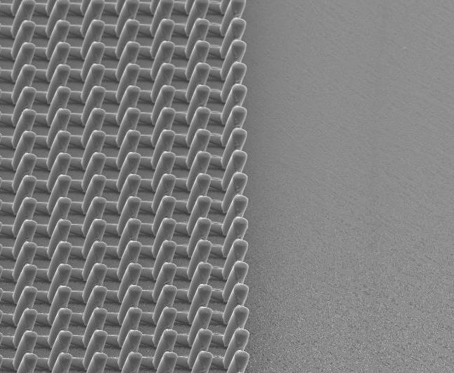
10 the PDMS solution is poured, is placed in a vacuum chamber shown in Fig. 2A, and the vacuum state is maintained for a predetermined time (for example, 1 minutes) so as to remove bubbles in the PDMS solution. After removing the bubbles in the PDMS solution, the pre-patterned silicon wafer with the PDMS solution thereon is placed on an optical table for a predetermined time (for example, 1 minutes) and the pre-patterned silicon wafer is then put in the horizontal state so as to make the surface of the PDMS solution smooth. Next, the pre-patterned silicon wafer in the horizontal state is heated on the hot plate at a predetermined temperature (for example, 7 C) for a predetermined time (for example, 7 minutes) so as to 1 solidify the PDMS solution on the pre-patterned silicon wafer. Next, the solidified PDMS solution on the prepatterned silicon wafer 2 is cooled at the room temperature for a predetermined time (for example, minutes) and then removed from the pre-patterned silicon wafer. Thus, a PDMS sample 1, which is a polymer material with a linear micropillar array as shown in Fig. 1A, is fabricated. The micropillar array includes 64 square pattern spaces having the horizontal and vertical lengths of 2 4 mm, in which four groups of 16 patterns are respectively formed. The micropillar array has a width in the range of 1 --
11 nm to mm and a length in the range of 1 nm to mm. For example, the first group has arranged pillars having a diameter of μm at intervals of μm, the second group has arranged pillars having a diameter of μm at intervals of μm, the third group has arranged walls having a thickness of μm and a length 4 mm at intervals of μm, and the fourth group has arranged pillars having a diameter of μm at intervals of μm. The patterns may be fabricated so as to have the same height of 30 μm. In this case, as shown in Fig. 2B, the PDMS sample 1, which is a polymer material with a linear micropillar array, is fixed onto a jig 7 at a predetermined tilt angle (α), such that the ion beams 3 are irradiated at a predetermined angle onto the surface of the PDMS sample 1 1 from the ion beam deposition apparatus. That is, the PDMS sample 1, which is a polymer material with a linear micropillar array, is disposed such that a predetermined angle is made between the PDMS sample 1 and the incident angle of the ion beams 3. A reference numeral 3 denotes a cathode to provide a bias voltage in the ion beam deposition apparatus. That is, Argon (Ar+) ion beam treatment using any one of the PECVD, PSII, filtered vacuum arc, atmospheric plasma treatment method and ion beam method is performed on the PDMS sample 1, which is a polymer 2 material with a linear micropillar array. The ion beam treatment is performed for minutes on the conditions that -11-
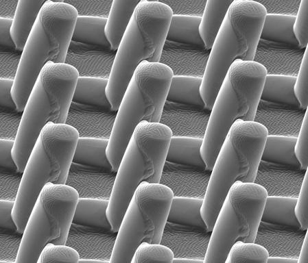
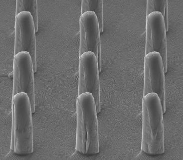
12 the voltage is at 400 V, and the degree of vacuum of the vacuum chamber is 0.49 Pa. As described above, if the ion beam treatment using the PECVD method or the like is performed on the surface of the PDMS sample 1, which is a polymer material with a linear micropillar array, the SEM image of the upright linear micropillar array shown in Fig. 3A is deformed to the SEM image of a tilted micropillar array in one direction shown in Fig. 3B due to compressive residual stress by the tilt angle (α), and wrinkles are formed. Specifically, if an ion beam or plasma is irradiated onto the surface of the PDMS sample 1, which is a polymer material with a micropillar array, the surface of the PDMS sample 1 is hardened about 0 times, and wrinkles are 1 generated due to compressive residual stress. In other words, as shown in Figs. 3C and 3D, the surface of a micropillar 30 which is directly influenced by the ion beams undergoes stress more than the opposing surface of the micropillar, causing compressive stress. Then, wrinkles 301 are generated, and the surface of the micropillar 30 tends to be contracted and shortened. Therefore, as shown in Fig. 3D, while wrinkles 301 are generated on the surface of the micropillar 30 where residual stress is produced, no wrinkles are generated on the opposing surface of the 2 micropillar 30 where ion beam or plasma does not reach owing to shadowing effect. As a result, the surface of the -12-
13 micropillar 30 is contracted, and thus the micropillar 30 is tilted in a direction in which the ion beams is irradiated. Fig. 4A shows an SEM image of a linear micro-pillar array before ion beam treatment is performed. Fig. 4B shows an SEM image of a tilted micropillar array, which is formed with an incident angle for ion beam treatment tilted at α=, according to the embodiment of the present invention. Fig. 4C shows an SEM image of a tilted micropillar array, which is formed with an incident angle for ion beam treatment tilted at α=40, according to the embodiment of the present invention. Figs. A and B show an SEM image where wrinkles are observed in a portion, in which no micropillar array is 1 formed, due to a change in voltage according to the embodiment of the present invention. Fig. C is a graph showing a wrinkle wavelength. The width and height of wrinkles 01, as can be seen in Figs. A and B, are closely associated with the ion beam energy for ion beam treatment. In particular, an increase in a bias voltage, which is the intensity of energy, causes an increase in the width of wrinkles in the polymer material. The wrinkles on the surface enable the micropillar array to be tilted. 2 Specifically, the reason why wrinkles are formed on the surface of the micropillar and the surface, on which no -13-
14 pillar array is formed, by ion beams for plasma treatment is that the surface of a soft polymer, such as PDMS, is hardened by the ion beams so as to form a skin layer, and the resultant skin layer and the existing polymer material are different in the elastic coefficient around 0 times. In this case, elastic energy caused by compressive stress is added, so nano-sized wrinkles are formed. Assuming that the elastic coefficient of an existing soft polymer is E s, and the elastic coefficient of the resultant skin layer having a thickness of h is E f, a critical deformation for forming wrinkles is expressed by the following equation. 1 [Equation 1] ε c = / 3 ( E / E ) s f For Equation 1, ε c is a critical deformation, E s is the elastic coefficient of the existing soft polymer, and E f is the elastic coefficient of the resultant skin layer. Referring to Equation 1, the critical deformation does not have to do with the thickness of the skin layer. An increase in the calculated critical deformation causes an increase in the amplitude of the wrinkle pattern having a sine wave shape. This is expressed by the following equation. [Equation 2] 2 A / h= 2 ( ε / ε c ) 1-14-
15 For Equation 2, ε is a deformation rate externally exerted. In this case, it can be seen that the deformation rate applied to the surface of the PDMS sample and the surface of the micropillar array linearly increases with the increase in the amplitude of the wrinkle pattern. That is, as shown in the graph of Fig. 6A showing a change in wavelength depending on the irradiation time and the graph of Fig. 6B showing a change in amplitude with the irradiation time when the bias voltage is constant at -400 V, an increase in the irradiation time of the ion beam for the ion beam treatment onto the surface of the polymer causes an increase in the amplitude of the wrinkle pattern, thus causing an increase in the applied deformation rate. For this reason, the 1 applied deformation rate can be quantitatively measured by measuring the amplitude of wrinkles to be formed. Therefore, an increase in the deformation rate of the micropillar array causes an increase in the amplitude of the wrinkle pattern, so the micropillar array is gradually tilted toward the progress direction of plasma. The wrinkle wavelength λ is in proportion to the thickness and has to do with the difference of elastic moduli between the ion beam induced skin (f) and PDMS (s). This is expressed by the following equation. 2 [Equation 3] λ / h α 1 / 3 ( E / ) f E s -1-
16 For Equation 3, the relationship α=4.36 is established under planar deformation condition. As described above, Equations 1 to 3 are appropriately used so as to analyze the skin and the wrinkles due to ion beams and plasma. Fig. 7A is a graph showing a tilt angle of a micropillar to an angle between a micropillar array and an ion beam for ion beam treatment according to the embodiment of the present invention. Fig. 7B shows an SEM image of a micropillar tilted at an angle α=40 according to the embodiment of the present invention. Fig. 7C shows an SEM image of a micropillar tilted at an angle α=80 according to the embodiment of the present invention. In this case, the width, height, and interval of each 1 pillar in the micropillar array are μm, 30 μm, and μm, respectively, and the total ion beam treatment time is 60 minutes under the energy condition that the anode voltage is 0 V and the bias voltage is -600 V. In this case, it can be seen that, as shown in Fig. 6A, if the angle of the micropillar array is α=0 or α=90, the micropillar array is not easily tilted, and at the angle α=40, the micropillar array is most tilted. This may be changed with the changes in the position of the micropillar array, the ion beam treatment time, and the energy condition. 2 According to the embodiment of the present invention, the tilted micropillar array can be formed by adjusting the -16-
17 incident angle of the ion beam for the ion beam treatment. Therefore, the present invention can be applied in manufacturing an adhesive material with dry self-cleaning, a micro robot which can go up the wall, a wafer aligner for a semiconductor manufacturing line, and the like. While the present invention has been shown and described with respect to the embodiment, it will be understood by those skilled in the art that various changes and modifications may be made without departing from the scope of the present invention as defined in the following claims. -17-
18 What is claimed is: 1. A polymer microstructure comprising: a polymer material with a linear micropillar array formed thereon, wherein the linear micropillar array is subjected to either thin film coating or sputtering of a gas and metal/non-metal material while adjusting an incident angle of an ion beam for ion beam treatment over the entire top surface of the linear micropillar array, to make the micropillar array be tilted. 2. The polymer microstructure of claim 1, wherein the linear micropillar array is formed in the shape of one of a 1 pillar, a dot, a hole, and a wall having a convex shape. 3. The polymer microstructure of claim 1, wherein the ion beam treatment is performed by one of PECVD (plasma-enhanced chemical vapor deposition) method, PSII (plasma source ion implantation), filtered vacuum arc, atmospheric plasma treatment method and ion beam method. 4. The polymer microstructure of claim 1, wherein the incident angle is an angle between an ion beam acceleration 2 direction in the ion beam treatment and the polymer material. -18-
19 . The polymer microstructure of claim 1, wherein the ion beam is one of argon gas, oxygen, N 2 (nitrogen), Xe (xenon), He (helium) and CF 4 (tetrafluoromethane). 6. The polymer microstructure of claim 1, wherein the ion beam for the ion beam treatment is irradiated obliquely in a predetermined direction so as to tilt the micropillar array in a predetermined direction. 7. The polymer microstructure of claim 1, wherein the angle of the tilted micropillar array is adjusted by controlled at least one of the incident angle, the irradiation time, and the magnitude of acceleration voltage of the ion beam for the ion beam treatment The polymer microstructure of claim 7, wherein the irradiation time of the ion beam for the ion beam treatment is controlled so as to adjust the asymmetric sectional shape of the tilted micropillar array. 9. The polymer microstructure of claim 7, wherein the acceleration voltage of the ion beam is in the range of 0 V to 0.0 kv. 2. The polymer microstructure of claim 1, wherein the incident angle of the ion beam for the ion beam treatment is -19-
20 equal to or more than 0 and equal to or less than The polymer microstructure of claim 1, wherein the tilted micropillar array has a width in the range of 1 nm to mm and a length in the range of 1 nm to mm. 12. A method of fabricating a polymer microstructure with a tilted micropillar array, the method comprising: forming a polymer sample with a linear micropillar array; fixing the polymer sample onto a jig having a predetermined tilt angle within a chamber; and performing ion beam treatment on the top surface of the linear micropillar array to form the tilted micropillar 1 array. 13. The method of claim 12, wherein the ion beam treatment is performed by one of a PECVD (plasma-enhanced chemical vapor deposition) method, PSII (plasma source ion implantation), filtered vacuum arc, atmospheric plasma treatment method and ion beam method. 14. The method of claim 12, wherein the ion beam is one of argon gas, oxygen, N 2 (nitrogen), Xe (xenon), He (helium) 2 and CF 4 (tetrafluoromethane). --
21 1. The method of claim 12, wherein the tilt angle of the tilted micropillar array is adjusted by controlling at least one of the incident angle, the irradiation time, the magnitude of acceleration voltage of the ion beam for the ion beam treatment. 16. The method of claim 12, wherein the pressure in the chamber for the ion beam treatment is in a range of Pa to Pa. 17. The method of claim 1, wherein the acceleration voltage of the ion beam for the ion beam treatment is in a range of 0 V to 0.0 kv The method of claim 1, wherein the incident angle of the ion beam for the ion beam treatment is equal to or more than 0 and equal to or less than The method of claim 12, wherein the tilted micropillar array has a width in the range of 1 nm to mm and a length in the range of 1 nm to mm.. The method of claim 12, wherein a material for the polymer sample includes one of PDMS (PolydiMethyl Siloxane), 2 polycarbonate (PC), polyimide (PI), polyethylene (PE), poly methyl methacrylate (PMMA), polystyrene (PS), poly lactic- -21-
22 co-glycolic acid (PLGA), hydrogel, polyethylene terephthalate (PET) and silicone rubber. -22-
23 ABSTRACT A polymer microstructure with a tilted micropillar array and a method of fabricating the same. The tilted micropillar array is formed by adjusting the incident angle of the ion beam for the ion beam treatment using a PECVD method with low energy consumption. The tilt angle of the micropillars is adjusted to a desired angle by adjusting at least one of the incident angle, the irradiation time, and the magnitude of acceleration voltage of the ion beam for the ion beam treatment. -23-
24 -24-
25 FIG. 1B -2-
26 -26-

27 FIG. 3A FIG. 3B -27-
28 -28-

29 FIG. 4A FIG. 4B -29-

30 FIG. 4C FIG. A -30-

31 FIG. B -31-
32 -32-
33 -33-

34 FIG. 7B FIG. 7C -34-
Supplementary Materials for
 www.sciencemag.org/cgi/content/full/science.1234855/dc1 Supplementary Materials for Taxel-Addressable Matrix of Vertical-Nanowire Piezotronic Transistors for Active/Adaptive Tactile Imaging Wenzhuo Wu,
Major Fabrication Steps in MOS Process Flow
 Major Fabrication Steps in MOS Process Flow UV light Mask oxygen Silicon dioxide photoresist exposed photoresist oxide Silicon substrate Oxidation (Field oxide) Photoresist Coating Mask-Wafer Alignment
CLAIMS 1. A suspension board with circuit, characterized in that, it comprises a metal support layer, an insulating layer formed on the metal support
 [19] State Intellectual Property Office of the P.R.C [51] Int. Cl 7 G11B 5/48 H05K 1/11 [12] Patent Application Publication G11B 21/16 [21] Application No.: 00133926.5 [43] Publication Date: 5.30.2001
Nanofluidic Diodes based on Nanotube Heterojunctions
 Supporting Information Nanofluidic Diodes based on Nanotube Heterojunctions Ruoxue Yan, Wenjie Liang, Rong Fan, Peidong Yang 1 Department of Chemistry, University of California, Berkeley, CA 94720, USA
Semiconductor Manufacturing Technology. Semiconductor Manufacturing Technology. Photolithography: Resist Development and Advanced Lithography
 Semiconductor Manufacturing Technology Michael Quirk & Julian Serda October 2001 by Prentice Hall Chapter 15 Photolithography: Resist Development and Advanced Lithography Eight Basic Steps of Photolithography
Lecture 7. Lithography and Pattern Transfer. Reading: Chapter 7
 Lecture 7 Lithography and Pattern Transfer Reading: Chapter 7 Used for Pattern transfer into oxides, metals, semiconductors. 3 types of Photoresists (PR): Lithography and Photoresists 1.) Positive: PR
EG2605 Undergraduate Research Opportunities Program. Large Scale Nano Fabrication via Proton Lithography Using Metallic Stencils
 EG2605 Undergraduate Research Opportunities Program Large Scale Nano Fabrication via Proton Lithography Using Metallic Stencils Tan Chuan Fu 1, Jeroen Anton van Kan 2, Pattabiraman Santhana Raman 2, Yao
Chapter 3 Fabrication
 Chapter 3 Fabrication The total structure of MO pick-up contains four parts: 1. A sub-micro aperture underneath the SIL The sub-micro aperture is used to limit the final spot size from 300nm to 600nm for
Part 5-1: Lithography
 Part 5-1: Lithography Yao-Joe Yang 1 Pattern Transfer (Patterning) Types of lithography systems: Optical X-ray electron beam writer (non-traditional, no masks) Two-dimensional pattern transfer: limited
MICROSTRUCTURING OF METALLIC LAYERS FOR SENSOR APPLICATIONS
 MICROSTRUCTURING OF METALLIC LAYERS FOR SENSOR APPLICATIONS Vladimír KOLAŘÍK, Stanislav KRÁTKÝ, Michal URBÁNEK, Milan MATĚJKA, Jana CHLUMSKÁ, Miroslav HORÁČEK, Institute of Scientific Instruments of the
Outline. 1 Introduction. 2 Basic IC fabrication processes. 3 Fabrication techniques for MEMS. 4 Applications. 5 Mechanics issues on MEMS MDL NTHU
 Outline 1 Introduction 2 Basic IC fabrication processes 3 Fabrication techniques for MEMS 4 Applications 5 Mechanics issues on MEMS 2.2 Lithography Reading: Runyan Chap. 5, or 莊達人 Chap. 7, or Wolf and
Module 11: Photolithography. Lecture 14: Photolithography 4 (Continued)
") Module 11: Photolithography Lecture 14: Photolithography 4 (Continued) 1 In the previous lecture, we have discussed the utility of the three printing modes, and their relative advantages and disadvantages.
Module 11: Photolithography Lecture 14: Photolithography 4 (Continued) 1 In the previous lecture, we have discussed the utility of the three printing modes, and their relative advantages and disadvantages.
Development of Nanoimprint Mold Using JBX-9300FS
 Development of Nanoimprint Mold Using JBX-9300FS Morihisa Hoga, Mikio Ishikawa, Naoko Kuwahara Tadahiko Takikawa and Shiho Sasaki Dai Nippon Printing Co., Ltd Research & Development Center Electronic Device
Photolithography I ( Part 1 )
") 1 Photolithography I ( Part 1 ) Chapter 13 : Semiconductor Manufacturing Technology by M. Quirk & J. Serda Bjørn-Ove Fimland, Department of Electronics and Telecommunication, Norwegian University of Science
1 Photolithography I ( Part 1 ) Chapter 13 : Semiconductor Manufacturing Technology by M. Quirk & J. Serda Bjørn-Ove Fimland, Department of Electronics and Telecommunication, Norwegian University of Science
Section 2: Lithography. Jaeger Chapter 2. EE143 Ali Javey Slide 5-1
 Section 2: Lithography Jaeger Chapter 2 EE143 Ali Javey Slide 5-1 The lithographic process EE143 Ali Javey Slide 5-2 Photolithographic Process (a) (b) (c) (d) (e) (f) (g) Substrate covered with silicon
Section 2: Lithography. Jaeger Chapter 2 Litho Reader. The lithographic process
 Section 2: Lithography Jaeger Chapter 2 Litho Reader The lithographic process Photolithographic Process (a) (b) (c) (d) (e) (f) (g) Substrate covered with silicon dioxide barrier layer Positive photoresist
Section 2: Lithography. Jaeger Chapter 2 Litho Reader. EE143 Ali Javey Slide 5-1
 Section 2: Lithography Jaeger Chapter 2 Litho Reader EE143 Ali Javey Slide 5-1 The lithographic process EE143 Ali Javey Slide 5-2 Photolithographic Process (a) (b) (c) (d) (e) (f) (g) Substrate covered
PROFILE CONTROL OF A BOROSILICATE-GLASS GROOVE FORMED BY DEEP REACTIVE ION ETCHING. Teruhisa Akashi and Yasuhiro Yoshimura
 Stresa, Italy, 25-27 April 2007 PROFILE CONTROL OF A BOROSILICATE-GLASS GROOVE FORMED BY DEEP REACTIVE ION ETCHING Teruhisa Akashi and Yasuhiro Yoshimura Mechanical Engineering Research Laboratory (MERL),
PHGN/CHEN/MLGN 435/535: Interdisciplinary Silicon Processing Laboratory. Simple Si solar Cell!
 Where were we? Simple Si solar Cell! Two Levels of Masks - photoresist, alignment Etch and oxidation to isolate thermal oxide, deposited oxide, wet etching, dry etching, isolation schemes Doping - diffusion/ion
Supplementary Information
 Supplementary Information Wireless thin film transistor based on micro magnetic induction coupling antenna Byoung Ok Jun 1, Gwang Jun Lee 1, Jong Gu Kang 1,2, Seung Uk Kim 1, Ji Woong Choi 1, Seung Nam
(12) United States Patent (10) Patent No.: US 6,211,068 B1
 United States Patent (10) Patent No.: US 6,211,068 B1") USOO6211068B1 (12) United States Patent (10) Patent No.: US 6,211,068 B1 Huang (45) Date of Patent: Apr. 3, 2001 (54) DUAL DAMASCENE PROCESS FOR 5,981,377 * 11/1999 Koyama... 438/633 MANUFACTURING INTERCONNECTS
USOO6211068B1 (12) United States Patent (10) Patent No.: US 6,211,068 B1 Huang (45) Date of Patent: Apr. 3, 2001 (54) DUAL DAMASCENE PROCESS FOR 5,981,377 * 11/1999 Koyama... 438/633 MANUFACTURING INTERCONNECTS
Caterpillar Locomotion inspired Valveless Pneumatic Micropump using Single Teardrop-shaped Elastomeric Membrane
 Electronic Supplementary Material (ESI) for Lab on a Chip. This journal is The Royal Society of Chemistry 2014 Supporting Information Caterpillar Locomotion inspired Valveless Pneumatic Micropump using
The Department of Advanced Materials Engineering. Materials and Processes in Polymeric Microelectronics
 The Department of Advanced Materials Engineering Materials and Processes in Polymeric Microelectronics 1 Outline Materials and Processes in Polymeric Microelectronics Polymeric Microelectronics Process
High throughput ultra-long (20cm) nanowire fabrication using a. wafer-scale nanograting template
 nanowire fabrication using a. wafer-scale nanograting template") Supporting Information High throughput ultra-long (20cm) nanowire fabrication using a wafer-scale nanograting template Jeongho Yeon 1, Young Jae Lee 2, Dong Eun Yoo 3, Kyoung Jong Yoo 2, Jin Su Kim 2,
Supporting Information High throughput ultra-long (20cm) nanowire fabrication using a wafer-scale nanograting template Jeongho Yeon 1, Young Jae Lee 2, Dong Eun Yoo 3, Kyoung Jong Yoo 2, Jin Su Kim 2,
Fabrication of micro structures on curve surface by X-ray lithography
 Fabrication of micro structures on curve surface by X-ray lithography Yigui Li 1, Susumu Sugiyama 2 Abstract We demonstrate experimentally the x-ray lithography techniques to fabricate micro structures
SUPPLEMENTARY INFORMATION
 SUPPLEMENTARY INFORMATION doi:10.1038/nature11293 1. Formation of (111)B polar surface on Si(111) for selective-area growth of InGaAs nanowires on Si. Conventional III-V nanowires (NWs) tend to grow in
Module 11: Photolithography. Lecture11: Photolithography - I
 Module 11: Photolithography Lecture11: Photolithography - I 1 11.0 Photolithography Fundamentals We will all agree that incredible progress is happening in the filed of electronics and computers. For example,
KMPR 1010 Process for Glass Wafers
 KMPR 1010 Process for Glass Wafers KMPR 1010 Steps Protocol Step System Condition Note Plasma Cleaning PVA Tepla Ion 10 5 mins Run OmniCoat Receipt Dehydration Any Heat Plate 150 C, 5 mins HMDS Coating
COMPARISON OF ULTIMATE RESOLUTION ACHIEVED BY E-BEAM WRITERS WITH SHAPED BEAM AND WITH GAUSSIAN BEAM
 COMPARISON OF ULTIMATE RESOLUTION ACHIEVED BY E-BEAM WRITERS WITH SHAPED BEAM AND WITH GAUSSIAN BEAM Stanislav KRÁTKÝ a, Vladimír KOLAŘÍK a, Milan MATĚJKA a, Michal URBÁNEK a, Miroslav HORÁČEK a, Jana
FABRICATION OF CMOS INTEGRATED CIRCUITS. Dr. Mohammed M. Farag
 FABRICATION OF CMOS INTEGRATED CIRCUITS Dr. Mohammed M. Farag Outline Overview of CMOS Fabrication Processes The CMOS Fabrication Process Flow Design Rules Reference: Uyemura, John P. "Introduction to
Lecture 13 Basic Photolithography
 Lecture 13 Basic Photolithography Chapter 12 Wolf and Tauber 1/64 Announcements Homework: Homework 3 is due today, please hand them in at the front. Will be returned one week from Thursday (16 th Nov).
Fabrication of concave gratings by curved surface UV-nanoimprint lithography
 Fabrication of concave gratings by curved surface UV-nanoimprint lithography Yung-Pin Chen, Yuet-Ping Lee, Jer-Haur Chang, and Lon A. Wang a Photonics and Nano-Structure Laboratory, Department of Electrical
SU-8 Post Development Bake (Hard Bake) Study
 Study") University of Pennsylvania ScholarlyCommons Protocols and Reports Browse by Type 10-16-2017 Ram Surya Gona University of Pennsylvania, ramgona@seas.upenn.edu Eric D. Johnston Singh Center for Nanotechnology,
University of Pennsylvania ScholarlyCommons Protocols and Reports Browse by Type 10-16-2017 Ram Surya Gona University of Pennsylvania, ramgona@seas.upenn.edu Eric D. Johnston Singh Center for Nanotechnology,
Advanced Plasma Technology. High precision film thickness trimming for the TFH industry. Roth & Rau AG September 2009
 Advanced Plasma Technology High precision film thickness trimming for the TFH industry Roth & Rau AG September 2009 Product Overview IonScan Equipment for ultra-precise Surface Processing IonScan 800 Wafer
Lithography. 3 rd. lecture: introduction. Prof. Yosi Shacham-Diamand. Fall 2004
 Lithography 3 rd lecture: introduction Prof. Yosi Shacham-Diamand Fall 2004 1 List of content Fundamental principles Characteristics parameters Exposure systems 2 Fundamental principles Aerial Image Exposure
CMOS Digital Integrated Circuits Lec 2 Fabrication of MOSFETs
 CMOS Digital Integrated Circuits Lec 2 Fabrication of MOSFETs 1 CMOS Digital Integrated Circuits 3 rd Edition Categories of Materials Materials can be categorized into three main groups regarding their
Module - 2 Lecture - 13 Lithography I
 Nano Structured Materials-Synthesis, Properties, Self Assembly and Applications Prof. Ashok. K.Ganguli Department of Chemistry Indian Institute of Technology, Delhi Module - 2 Lecture - 13 Lithography
Dr. Dirk Meyners Prof. Wagner. Wagner / Meyners Micro / Nanosystems Technology
 Micro/Nanosystems Technology Dr. Dirk Meyners Prof. Wagner 1 Outline - Lithography Overview - UV-Lithography - Resolution Enhancement Techniques - Electron Beam Lithography - Patterning with Focused Ion
Supporting Information. High-Resolution Organic Light Emitting Diodes Patterned via Contact Printing
 Supporting Information High-Resolution Organic Light Emitting Diodes Patterned via Contact Printing Jinhai Li, Lisong Xu, Ching W. Tang and Alexander A. Shestopalov* Department of Chemical Engineering,
(12) Patent Application Publication (10) Pub. No.: US 2005/ A1
 Patent Application Publication (10) Pub. No.: US 2005/ A1") US 20050207013A1 (19) United States (12) Patent Application Publication (10) Pub. No.: US 2005/0207013 A1 Kanno et al. (43) Pub. Date: Sep. 22, 2005 (54) PHOTOELECTRIC ENCODER AND (30) Foreign Application
US 20050207013A1 (19) United States (12) Patent Application Publication (10) Pub. No.: US 2005/0207013 A1 Kanno et al. (43) Pub. Date: Sep. 22, 2005 (54) PHOTOELECTRIC ENCODER AND (30) Foreign Application
420 Intro to VLSI Design
 Dept of Electrical and Computer Engineering 420 Intro to VLSI Design Lecture 0: Course Introduction and Overview Valencia M. Joyner Spring 2005 Getting Started Syllabus About the Instructor Labs, Problem
Soft Electronics Enabled Ergonomic Human-Computer Interaction for Swallowing Training
 Supplementary Information Soft Electronics Enabled Ergonomic Human-Computer Interaction for Swallowing Training Yongkuk Lee 1,+, Benjamin Nicholls 2,+, Dong Sup Lee 1, Yanfei Chen 3, Youngjae Chun 3,4,
Profile Measurement of Resist Surface Using Multi-Array-Probe System
 Sensors & Transducers 2014 by IFSA Publishing, S. L. http://www.sensorsportal.com Profile Measurement of Resist Surface Using Multi-Array-Probe System Shujie LIU, Yuanliang ZHANG and Zuolan YUAN School
Niobium Coating of Copper Cavities by UHV Cathodic Arc: progress report
 Niobium Coating of Copper Cavities by UHV Cathodic Arc: progress report L. Catani, A. Cianchi, D. Digiovenale, J. Lorkiewicz, Prof. S. Tazzari, INFN-Roma "Tor Vergata", Italy Roberto Russo, Istituto di
MICRO YAW RATE SENSORS
 1 MICRO YAW RATE SENSORS FIELD OF THE INVENTION This invention relates to micro yaw rate sensors suitable for measuring yaw rate around its sensing axis. More particularly, to micro yaw rate sensors fabricated
Fabrication Techniques of Optical ICs
 Fabrication Techniques of Optical ICs Processing Techniques Lift off Process Etching Process Patterning Techniques Photo Lithography Electron Beam Lithography Photo Resist ( Microposit MP1300) Electron
Romano et al. [45] Date of Patent: May 12, 1998
![Romano et al. [45] Date of Patent: May 12, 1998](/thumbs/94/120092598.jpg "Romano et al. [45] Date of Patent: May 12, 1998") 1111111111111111111111111111111111111111111111111111111I1111111111111111111 US005750202A United States Patent [19] [11] Patent Number: 5,750,202 Romano et al. [45] Date of Patent: May 12, 1998 [54] PREPARATION
1111111111111111111111111111111111111111111111111111111I1111111111111111111 US005750202A United States Patent [19] [11] Patent Number: 5,750,202 Romano et al. [45] Date of Patent: May 12, 1998 [54] PREPARATION
EE143 Fall 2016 Microfabrication Technologies. Lecture 3: Lithography Reading: Jaeger, Chap. 2
 EE143 Fall 2016 Microfabrication Technologies Lecture 3: Lithography Reading: Jaeger, Chap. 2 Prof. Ming C. Wu wu@eecs.berkeley.edu 511 Sutardja Dai Hall (SDH) 1-1 The lithographic process 1-2 1 Photolithographic
(12) Patent Application Publication (10) Pub. No.: US 2004/ A1
 Patent Application Publication (10) Pub. No.: US 2004/ A1") US 2004O155237A1 (19) United States (12) Patent Application Publication (10) Pub. No.: US 2004/0155237 A1 Kerber (43) Pub. Date: Aug. 12, 2004 (54) SELF-ALIGNED JUNCTION PASSIVATION Publication Classification
US 2004O155237A1 (19) United States (12) Patent Application Publication (10) Pub. No.: US 2004/0155237 A1 Kerber (43) Pub. Date: Aug. 12, 2004 (54) SELF-ALIGNED JUNCTION PASSIVATION Publication Classification
Coating of Si Nanowire Array by Flexible Polymer
 , pp.422-426 http://dx.doi.org/10.14257/astl.2016.139.84 Coating of Si Nanowire Array by Flexible Polymer Hee- Jo An 1, Seung-jin Lee 2, Taek-soo Ji 3* 1,2.3 Department of Electronics and Computer Engineering,
Transparent p-type SnO Nanowires with Unprecedented Hole Mobility among Oxide Semiconductors
 Supplementary Information Transparent p-type SnO Nanowires with Unprecedented Hole Mobility among Oxide Semiconductors J. A. Caraveo-Frescas and H. N. Alshareef* Materials Science and Engineering, King
Triple Beam FIB-SEM-Ar(Xe) Combined System NX2000
 Combined System NX2000") SCIENTIFIC INSTRUMENT NEWS 2017 Vol. 8 M A R C H Technical magazine of Electron Microscope and Analytical Instruments. Technical Explanation Triple Beam FIB-SEM-Ar(Xe) Combined System NX2000 Masahiro Kiyohara
SCIENTIFIC INSTRUMENT NEWS 2017 Vol. 8 M A R C H Technical magazine of Electron Microscope and Analytical Instruments. Technical Explanation Triple Beam FIB-SEM-Ar(Xe) Combined System NX2000 Masahiro Kiyohara
Inkjet Printing of Ag Nanoparticles using Dimatix Inkjet Printer, No 1
 University of Pennsylvania ScholarlyCommons Protocols and Reports Browse by Type 1-13-2017 using Dimatix Inkjet Printer, No 1 Amal Abbas amalabb@seas.upenn.edu Inayat Bajwa inabajwa@seas.upenn.edu Follow
Microlens formation using heavily dyed photoresist in a single step
 Microlens formation using heavily dyed photoresist in a single step Chris Cox, Curtis Planje, Nick Brakensiek, Zhimin Zhu, Jonathan Mayo Brewer Science, Inc., 2401 Brewer Drive, Rolla, MO 65401, USA ABSTRACT
*EP A1* EP A1 (19) (11) EP A1 (12) EUROPEAN PATENT APPLICATION. (43) Date of publication: Bulletin 2005/21
 (11) EP A1 (12) EUROPEAN PATENT APPLICATION. (43) Date of publication: Bulletin 2005/21") (19) Europäisches Patentamt European Patent Office Office européen des brevets *EP0013367A1* (11) EP 1 33 67 A1 (12) EUROPEAN PATENT APPLICATION (43) Date of publication: 2.0.200 Bulletin 200/21 (1) Int
(19) Europäisches Patentamt European Patent Office Office européen des brevets *EP0013367A1* (11) EP 1 33 67 A1 (12) EUROPEAN PATENT APPLICATION (43) Date of publication: 2.0.200 Bulletin 200/21 (1) Int
Measurement of Microscopic Three-dimensional Profiles with High Accuracy and Simple Operation
 238 Hitachi Review Vol. 65 (2016), No. 7 Featured Articles Measurement of Microscopic Three-dimensional Profiles with High Accuracy and Simple Operation AFM5500M Scanning Probe Microscope Satoshi Hasumura
plasmonic nanoblock pair
 Nanostructured potential of optical trapping using a plasmonic nanoblock pair Yoshito Tanaka, Shogo Kaneda and Keiji Sasaki* Research Institute for Electronic Science, Hokkaido University, Sapporo 1-2,
Obducat NIL 6. Nanoimprinting with NRF s NIL 6
 Obducat NIL 6 Substrates: pieces to 6 inch, hard or soft Thermal cure with PMMA, MR I 7010 etc Alignment to about 3 microns Temperature to 300 HC Pressure 15 to 80 bars Resolution < 50 nm possible Up to
Surface Topography and Alignment Effects in UV-Modified Polyimide Films with Micron Size Patterns
 CHINESE JOURNAL OF PHYSICS VOL. 41, NO. 2 APRIL 2003 Surface Topography and Alignment Effects in UV-Modified Polyimide Films with Micron Size Patterns Ru-Pin Pan 1, Hua-Yu Chiu 1,Yea-FengLin 1,andJ.Y.Huang
Rapid and inexpensive fabrication of polymeric microfluidic devices via toner transfer masking
 Easley et al. Toner Transfer Masking Page -1- B816575K_supplementary_revd.doc December 3, 2008 Supplementary Information for Rapid and inexpensive fabrication of polymeric microfluidic devices via toner
Fabrication of plastic microlens array using gas-assisted micro-hot-embossing with a silicon mold
 Infrared Physics & Technology 48 (2006) 163 173 www.elsevier.com/locate/infrared Fabrication of plastic microlens array using gas-assisted micro-hot-embossing with a silicon mold C.-Y. Chang a, S.-Y. Yang
A large-area wireless power transmission sheet using printed organic. transistors and plastic MEMS switches
 Supplementary Information A large-area wireless power transmission sheet using printed organic transistors and plastic MEMS switches Tsuyoshi Sekitani 1, Makoto Takamiya 2, Yoshiaki Noguchi 1, Shintaro
SCINTILLATING FIBER DOSIMETER ARRAY
 SCINTILLATING FIBER DOSIMETER ARRAY FIELD OF THE INVENTION [0001] This invention relates generally to the field of dosimetry and, more particularly, to rapid, high-resolution dosimeters for advanced treatment
VLSI Design. Introduction
 VLSI Design Introduction Outline Introduction Silicon, pn-junctions and transistors A Brief History Operation of MOS Transistors CMOS circuits Fabrication steps for CMOS circuits Introduction Integrated
SCANNING ELECTRON MICROSCOPE (SEM) INSPECTION OF SEMICONDUCTOR DICE. ESCC Basic Specification No
 INSPECTION OF SEMICONDUCTOR DICE. ESCC Basic Specification No") Page 1 of 24 SCANNING ELECTRON MICROSCOPE (SEM) INSPECTION OF SEMICONDUCTOR DICE ESCC Basic Specification Issue 2 February 2014 Document Custodian: European Space Agency see https://escies.org PAGE 2 LEGAL
Page 1 of 24 SCANNING ELECTRON MICROSCOPE (SEM) INSPECTION OF SEMICONDUCTOR DICE ESCC Basic Specification Issue 2 February 2014 Document Custodian: European Space Agency see https://escies.org PAGE 2 LEGAL
Semiconductor Technology
 Semiconductor Technology from A to Z + - x 1 0 x Photolithographie www.halbleiter.org Contents Contents List of Figures III 1 Photolithographie 1 1.1 Exposure and resist coating..........................
CARESTREAM INDUSTREX Digital Imaging Plates
 2016-09-29 TI-2632 CARESTREAM INDUSTREX Digital Imaging Plates CARESTREAM INDUSTREX Flex Digital Imaging Plates (IPs) are designed for computed radiography in nondestructive testing applications. These
Optical Bus for Intra and Inter-chip Optical Interconnects
 Optical Bus for Intra and Inter-chip Optical Interconnects Xiaolong Wang Omega Optics Inc., Austin, TX Ray T. Chen University of Texas at Austin, Austin, TX Outline Perspective of Optical Backplane Bus
A New Profile Measurement Method for Thin Film Surface
 Send Orders for Reprints to reprints@benthamscience.ae 480 The Open Automation and Control Systems Journal, 2014, 6, 480-487 A New Profile Measurement Method for Thin Film Surface Open Access ShuJie Liu
Figure 7 Dynamic range expansion of Shack- Hartmann sensor using a spatial-light modulator
 Figure 4 Advantage of having smaller focal spot on CCD with super-fine pixels: Larger focal point compromises the sensitivity, spatial resolution, and accuracy. Figure 1 Typical microlens array for Shack-Hartmann
College of Engineering Department of Electrical Engineering and Computer Sciences University of California, Berkeley
 College of Engineering Department of Electrical Engineering and Below are your weekly quizzes. You should print out a copy of the quiz and complete it before your lab section. Bring in the completed quiz
CHAPTER 2 Principle and Design
 CHAPTER 2 Principle and Design The binary and gray-scale microlens will be designed and fabricated. Silicon nitride and photoresist will be taken as the material of the microlens in this thesis. The design
Photoresist erosion studied in an inductively coupled plasma reactor employing CHF 3
 Photoresist erosion studied in an inductively coupled plasma reactor employing CHF 3 M. F. Doemling, N. R. Rueger, and G. S. Oehrlein a) Department of Physics, University at Albany, State University of
Micro- and Nano- Fabrication and Replication Techniques
 Micro- and Nano- Fabrication and Replication Techniques Why do we have to write thing small and replicate fast? Plenty of Room at the Bottom Richard P. Feynman, December 1959 How do we write it? We have
(12) Patent Application Publication (10) Pub. No.: US 2016/ A1
 Patent Application Publication (10) Pub. No.: US 2016/ A1") US 201601 11776A1 (19) United States (12) Patent Application Publication (10) Pub. No.: US 2016/0111776 A1 OKUMURA et al. (43) Pub. Date: Apr. 21, 2016 (54) RADIO WAVE TRANSMISSIVECOVER (30) Foreign Application
US 201601 11776A1 (19) United States (12) Patent Application Publication (10) Pub. No.: US 2016/0111776 A1 OKUMURA et al. (43) Pub. Date: Apr. 21, 2016 (54) RADIO WAVE TRANSMISSIVECOVER (30) Foreign Application
Multi-Wire Drift Chambers (MWDC)
") Multi-Wire Drift Chambers (MWDC) Mitra Shabestari August 2010 Introduction The detailed procedure for construction of multi-wire drift chambers is presented in this document. Multi-Wire Proportional Counters
Multi-Wire Drift Chambers (MWDC) Mitra Shabestari August 2010 Introduction The detailed procedure for construction of multi-wire drift chambers is presented in this document. Multi-Wire Proportional Counters
A Laser-Based Thin-Film Growth Monitor
 TECHNOLOGY by Charles Taylor, Darryl Barlett, Eric Chason, and Jerry Floro A Laser-Based Thin-Film Growth Monitor The Multi-beam Optical Sensor (MOS) was developed jointly by k-space Associates (Ann Arbor,
(12) Patent Application Publication (10) Pub. No.: US 2014/ A1
 Patent Application Publication (10) Pub. No.: US 2014/ A1") (19) United States US 20140097081A1 (12) Patent Application Publication (10) Pub. No.: US 2014/0097081 A1 Morrissey et al. (43) Pub. Date: (54) METHODS OF FORMING ATHIN FILM (52) U.S. Cl. RESISTOR USPC...
(19) United States US 20140097081A1 (12) Patent Application Publication (10) Pub. No.: US 2014/0097081 A1 Morrissey et al. (43) Pub. Date: (54) METHODS OF FORMING ATHIN FILM (52) U.S. Cl. RESISTOR USPC...
RANDY W. ALKIRE, GEROLD ROSENBAUM AND GWYNDAF EVANS
 S-94,316 PATENTS-US-A96698 BEAM POSITION MONITOR RANDY W. ALKIRE, GEROLD ROSENBAUM AND GWYNDAF EVANS CONTRACTUAL ORIGIN OF THE INVENTION The United States Government has rights in this invention pursuant
Optical Issues in Photolithography
 OpenStax-CNX module: m25448 1 Optical Issues in Photolithography Andrew R. Barron This work is produced by OpenStax-CNX and licensed under the Creative Commons Attribution License 3.0 note: This module
UFNF YES Image Reversal & HMDS Oven Revision 6.0 1/22/2014 Page 1 of 5. YES Image Reversal and HMDS Oven SOP
 1/22/2014 Page 1 of 5 YES Image Reversal and HMDS Oven SOP Table of Contents 1.0 Safety 2.0 Quality Control and Calibrations 3.0 Processes Description 4.0 Process Information for Lift Off 5.0 Operation
Supporting Information
 Electronic Supplementary Material (ESI) for Materials Horizons. This journal is The Royal Society of Chemistry 2017 Supporting Information Nanofocusing of circularly polarized Bessel-type plasmon polaritons
Rapid fabrication of ultraviolet-cured polymer microlens arrays by soft roller stamping process
 Microelectronic Engineering 84 (2007) 355 361 www.elsevier.com/locate/mee Rapid fabrication of ultraviolet-cured polymer microlens arrays by soft roller stamping process Chih-Yuan Chang, Sen-Yeu Yang *,
Applications of Cold Cathode PIG Ion Source in Lithography
 Applications of Cold Cathode PIG Ion Source in Lithography N. I. Bassal Accelerator Department, Nuclear research Center, AE A, Cairo, Egypt. Email/nagatbassal@yahoo.com Received: 7/12/2011 Accepted: 17/10/2012
CO3C 25/06. Manning. 2,841,477 7/1958 Hall... 41/42. 3,113,896 12/1963 Mann /3
 United States Patent (19) Banks et al. 54 ION BEAM SPUTTERETCHING (75) Inventors: Bruce A. Banks, Olmsted Township, Cuyahoga County; Sharon K. Rutledge, Bedford, both of Ohio 73) Assignee: The United States
EE4800 CMOS Digital IC Design & Analysis. Lecture 1 Introduction Zhuo Feng
 EE4800 CMOS Digital IC Design & Analysis Lecture 1 Introduction Zhuo Feng 1.1 Prof. Zhuo Feng Office: EERC 730 Phone: 487-3116 Email: zhuofeng@mtu.edu Class Website http://www.ece.mtu.edu/~zhuofeng/ee4800fall2010.html
Monolithically integrated InGaAs nanowires on 3D. structured silicon-on-insulator as a new platform for. full optical links
 Monolithically integrated InGaAs nanowires on 3D structured silicon-on-insulator as a new platform for full optical links Hyunseok Kim 1, Alan C. Farrell 1, Pradeep Senanayake 1, Wook-Jae Lee 1,* & Diana.
Supporting Information for. Stretchable Microfluidic Radio Frequency Antenna
 Supporting Information for Stretchable Microfluidic Radio Frequency Antenna Masahiro Kubo 1, Xiaofeng Li 2, Choongik Kim 1, Michinao Hashimoto 1, Benjamin J. Wiley 1, Donhee Ham 2 and George M. Whitesides
Exhibit 2 Declaration of Dr. Chris Mack
 STC.UNM v. Intel Corporation Doc. 113 Att. 5 Exhibit 2 Declaration of Dr. Chris Mack Dockets.Justia.com UNITED STATES DISTRICT COURT DISTRICT OF NEW MEXICO STC.UNM, Plaintiff, v. INTEL CORPORATION Civil
Waveguiding in PMMA photonic crystals
 ROMANIAN JOURNAL OF INFORMATION SCIENCE AND TECHNOLOGY Volume 12, Number 3, 2009, 308 316 Waveguiding in PMMA photonic crystals Daniela DRAGOMAN 1, Adrian DINESCU 2, Raluca MÜLLER2, Cristian KUSKO 2, Alex.
Lecture 0: Introduction
 Lecture 0: Introduction Introduction Integrated circuits: many transistors on one chip. Very Large Scale Integration (VLSI): bucketloads! Complementary Metal Oxide Semiconductor Fast, cheap, low power
Low-power carbon nanotube-based integrated circuits that can be transferred to biological surfaces
 SUPPLEMENTARY INFORMATION Articles https://doi.org/10.1038/s41928-018-0056-6 In the format provided by the authors and unedited. Low-power carbon nanotube-based integrated circuits that can be transferred
MICRO AND NANOPROCESSING TECHNOLOGIES
 MICRO AND NANOPROCESSING TECHNOLOGIES LECTURE 4 Optical lithography Concepts and processes Lithography systems Fundamental limitations and other issues Photoresists Photolithography process Process parameter
Supplementary Figure 1 Schematic illustration of fabrication procedure of MoS2/h- BN/graphene heterostructures. a, c d Supplementary Figure 2
 Supplementary Figure 1 Schematic illustration of fabrication procedure of MoS 2 /hon a 300- BN/graphene heterostructures. a, CVD-grown b, Graphene was patterned into graphene strips by oxygen monolayer
Sidewall lithography of micron-sized features in high-aspect-ratio meso-scale channels using a three-dimensional assembled mask
 Ji et al. Micro and Nano Systems Letters 2014, 2:6 LETTER Open Access Sidewall lithography of micron-sized features in high-aspect-ratio meso-scale channels using a three-dimensional assembled mask Chang-Hyeon
Optical Requirements
 Optical Requirements Transmission vs. Film Thickness A pellicle needs a good light transmission and long term transmission stability. Transmission depends on the film thickness, film material and any anti-reflective
32nm High-K/Metal Gate Version Including 2nd Generation Intel Core processor family
 From Sand to Silicon Making of a Chip Illustrations 32nm High-K/Metal Gate Version Including 2nd Generation Intel Core processor family April 2011 1 The illustrations on the following foils are low resolution
Photolithography Technology and Application
 Photolithography Technology and Application Jeff Tsai Director, Graduate Institute of Electro-Optical Engineering Tatung University Art or Science? Lind width = 100 to 5 micron meter!! Resolution = ~ 3
United States Patent Patent Number: 5,683,539 Qian et al. 45 Date of Patent: Nov. 4, 1997
 USOO5683539A United States Patent 19 11 Patent Number: Qian et al. 45 Date of Patent: Nov. 4, 1997 54 NDUCTIVELY COUPLED RF PLASMA 5,458,732 10/1995 Butler et al.... 216/61 REACTORWTH FLOATING COL 5,525,159
State-of-the-art device fabrication techniques
 State-of-the-art device fabrication techniques! Standard Photo-lithography and e-beam lithography! Advanced lithography techniques used in semiconductor industry Deposition: Thermal evaporation, e-gun