ICA & HDL SIMULATION
|
|
|
- Sharlene Hunt
- 5 years ago
- Views:
Transcription

1 ICA & HDL SIMULATION LABORATORY MANUAL III I SEMESTER Prepared By Mr. K.Murali Krishna, Associate Professor Mrs. S.Rajani, Assistant Professor DEPARTMENT OF ELECTRONICS AND COMMUNICATIONS ENGG MALLA REDDY COLLEGE OF ENGINEERING AND TECHNOLOGY (Sponsored by CMR Educational Society) (Affiliated to JNTU, Hyderabad) Secunderabad- 14.
2 CONTENTS CYCLE-I S.No. Experiment Name Page No. 1 INTRODUCTION - STUDY OF IC741, IC555 & IC OP-AMP APPLICATIONS ADDER, SUBTRACTOR, COMPARATOR 8 3 INTEGRATOR AND DIFFERENTIATOR USING IC741 OP-AMP 13 4 ACTIVE FILTER APPLICATIONS LPF AND HPF(1 ST ORDER) 18 5 IC741 WAVEFORM GENERATORS SINE, SQAURE AND 26 TRIANGULAR WAVES 6 IC555 TIMER MONOSTABLE AND ASTABLE MULTIVIBRATORS 31 7 SCHMITT TRIGGER CIRCUIT USING IC IC 565 PLL APPLICATIONS 41 9 VOLTAGE REGULATORS USING IC 723, THREE TERMINAL 44 VOLTAGE REGULATORS 7805, 7809 AND 7912 CYCLE-II S.No. Experiment Name Page No. 1 INTRODUCTION - Xilinx 52 2 HDL CODE TO REALIZE ALL LOGIC GATES 61 3 DESIGN OF 2-TO-4 ENCODER 63 4 DESIGN OF 8-TO-3 ENCODER 65 5 DESIGN OF 8-TO-1 MULTIPLEXER AND 1X8 DEMULTIPLEXER 67
3 6 DESIGN OF 4 BIT BINARY TO GRAY CODE CONVERTER 70 7 DESIGN OF 4-BIT COMPARATOR 72 8 DESIGN OF FULL ADDER USING THREE MODELLING STYLES 74 9 DESIGN OF FLIP FLOPS (SR,JK,D,T) DESIGN OF 4 BIT BINARY,BCD COUNTERS(SYNCHRONUS AND 83 ASYNCHRONUS RESET) 11 FINITE STATE MACHINE DESIGN 86


4 VISION MISSION QUALITY POLICY
5 PROGRAMME EDUCATIONAL OBJECTIVES PEO1: PROFESSIONALISM & CITIZENSHIP To create and sustain a community of learning in which students acquire knowledge and learn to apply it professionally with due consideration for ethical, ecological and economic issues. PEO2: TECHNICAL ACCOMPLISHMENTS To provide knowledge based services to satisfy the needs of society and the industry by providing hands on experience in various technologies in core field. PEO3: INVENTION, INNOVATION AND CREATIVITY To make the students to design, experiment, analyze, interpret in the core field with the help of other multi disciplinary concepts wherever applicable. PEO4: PROFESSIONAL DEVELOPMENT To educate the students to disseminate research findings with good soft skills and become a successful entrepreneur. PEO5: HUMAN RESOURCE DEVELOPMENT To graduate the students in building national capabilities in technology, education and research.
6 CODE OF CONDUCT FOR THE LABORATORIES All students must observe the Dress Code while in the laboratory. Sandals or open-toed shoes are NOT allowed. Foods, drinks and smoking are NOT allowed. All bags must be left at the indicated place. The lab timetable must be strictly followed. Be PUNCTUAL for your laboratory session. Program must be executed within the given time. Noise must be kept to a minimum. Workspace must be kept clean and tidy at all time. Handle the systems and interfacing kits with care. All students are liable for any damage to the accessories due to their own negligence. All interfacing kits connecting cables must be RETURNED if you taken from the lab supervisor. Students are strictly PROHIBITED from taking out any items from the laboratory. Students are NOT allowed to work alone in the laboratory without the Lab Supervisor USB Ports have been disabled if you want to use USB drive consult lab supervisor. Report immediately to the Lab Supervisor if any malfunction of the accessories, is there. Before leaving the lab Place the chairs properly. Turn off the system properly Turn off the monitor. Please check the laboratory notice board regularly for updates.
7 CYCLE - I 1
 & IC565.")

8 INTRODUCTION STUDY OF IC741, IC555 & IC565 AIM: To study pin details, specifications, applications and features of IC741 (Op-Amp) IC555 (Timer) & IC565. COMPONENTS: IC741, IC555 & IC565 IC741: (OPERATIONAL AMPLIFIER) Symbol: PIN CONFIGURATION: SPECIFICATIONS: Supply Voltage Internal Power Dissipation Differential input voltage Input Voltage 18V 310mw 30V 15V Operating temperature range 0ºC to 70ºC APPLICATIONS: Non-inverting amplifier Inverting amplifier Integrator, Differentiator Low Pass, High Pass, Band pass and Band Reject Filters 2


 PIN CONFIGURATION:")
9 FEATURES: No External frequency compensation is required Short circuit Protection Off Set Null Capability Large Common mode and differential Voltage ranges Low Power Dissipation No-Latch up Problem 741 is available in three packages: 8-pin metal can, 10-pin flat pack and 8 or 14-pin DIP IC555: (TIMER) PIN CONFIGURATION: FUNCTIONAL BLOCK DIAGRAM: 3

10 SPECIFICATIONS Supply Voltage Maximum Current rating 200mA 5V to 18V Minimum Triggering Voltage - (1/3) VCC Operating temperature range 0ºC to 70ºC APPLICATIONS: 1. Astable Multivibrator, Schmitt trigger, Free running ramp Generator, etc., 2. Monostable Multivibrator, Frequency divider, Pulse structure FEATURES: 555 timers are reliable, easy to use and low cost. The device is available as an 8 pin circular style, an 8 pin mini DIP or a 14 Pin DIP IC565: PHASE LOCKED LOOP (PLL) PIN CONFIGURATION 4

11 FUNCTIONAL BLOCK DIAGRAM MONOLITHIC PLL CHARACTERISTICS Operating frequency range: Hz to 500 khz. Operating voltage range: ± 6 to ± 12 V. Input impedance: 10 k Q typically. Output sink current: 1mA typically. Output source current: 10 m A typically. Drift in VCO centre frequency with temperature: 300 ppm/ C typically. Drift in VCO centre frequency with supply voltage: 1.5 %/V maximum. Input level required for tracking: 10 mvrms minimum to 3 V peak -to-peak maximum. Bandwidth adjustment range: < ± 1 to > ± 60 %. APPLICATIONS: 1. Modems 2. FSK Demodulation 3. FM Demodulation 4. Frequency Synthasizers etc. 5
12 QUESTIONS: 1. What is the symbol of op-amp? 2. Draw the pin diagram of op-amp. 3. What is the supply voltage range that an op-amp can with stand? 4. What is the input voltage range that an op-amp can with stand? 5. What are the available package types of IC741? 6. What is a virtual ground? What are the differences between the physical ground and the virtual ground? 7. What is the current flowing through the input terminals of an Ideal op-amp? 8. Which loop voltage gain is larger, closed or open? 9. What is the normal value of saturation voltage of an op-amp? 10. Mention a few applications of op-amp. 11. Mention some features of op-amp. 12. What is the main purpose of IC555 timer? 13. Draw the pin diagram of op-amp. 14. Draw the functional diagram of IC555 timer. 15. How many comparators are present in IC555 timer? 16. What are the trigger voltages of UC and LC? 17. What is the functionality of power amplifier in the output stage of IC555 timer? 18. Which is the Flip-Flop used in IC555 timer? 19. What is the use of RESET pin in IC555 timer? 20. What are the available package types of IC555 timer? 21. Mention a few applications of IC555 timer. 22. What is the dc level required for the negative going trigger pulse at pin 2 of IC555 timer? 23. What is IC565? 24. Draw the pin diagram of IC565 6
13 EXPERIMENT NO: 1 DATE: OP-AMP APPLICATIONS - ADDER, SUBTRACTOR & COMPARATOR AIM: To study Adder, Subtractor & Comparator circuits using OP-AMP IC741 and verify their theoretical and practical output. APPARATUS: Bread Board IC741, Resistors DC Supply Function Generator Multi meter CRO Probes, Connecting Wires THEORY: ADDER: Op-amp can be used to design a circuit whose output is the sum of several input signals. Such a circuit is called a summing amplifier or an adder. Summing amplifier can be classified as inverting & non-inverting summer depending on the input applied to inverting & non-inverting terminals respectively. Circuit Diagram shows a non-inverting adder with n inputs. Here the output will be the linear summation of input voltages. The circuit can be used either as summing amplifier, scaling amplifier, or as averaging amplifier. From the circuit of adder, it can be noted that at pin3 I 1 +I 2 +I 3 +.I n =0 V a = =0 =0 V o Va V o ( ) V o = (1+ ) ( ) 7

14 = (1+ (n-1)) ( ) =n ( ) V o = V 1 +V 2 +V 3 + +V n This means that the output voltage is equal to the sum of all the input voltages. SUBTRACTOR: A subtractor is a circuit that gives the difference of the two inputs, V o =V 2 -V 1, Where V 1 and V 2 are the inputs. By connecting one input voltage V 1 to inverting terminal and another input voltage V 2 to the non inverting terminal, we get the resulting circuit as the Subtractor. This is also called as differential or difference amplifier using op-amps. Output of a differential amplifier (subtractor) is given as V o = (-R f /R 1 ) (V 1 -V 2 ) If all external resistors are equal in value, then the gain of the amplifier is equal to -1. The output voltage of the differential amplifier with a gain of -1 is V o = (V 2 -V 1 ) Thus the output voltage V o is equal to the voltage V 2 applied to the non inverting terminal minus the voltage V 1 applied to the inverting terminal. Hence the circuit is called a Subtractor. COMPARATOR: A Comparator is a non-linear signal processor. It is an open loop mode application of Op-amp operated in saturation mode. Comparator compares a signal voltage at one input with a reference voltage at the other input. Here the Op-amp is operated in open loop mode and hence the output is ±V sat. It is basically classified as inverting and non-inverting comparator. In a non-inverting comparator V in is given to +ve terminal and V ref to ve terminal. When V in < V ref, the output is V sat and when V in > V ref, the output is +V sat (see expected waveforms). In an inverting comparator input is given to the inverting terminal and reference voltage is given to the non inverting terminal. The output of the inverting comparator is the inverse of the output of non-inverting comparator. The comparator can be used as a zero crossing detector, window detector, time marker generator and phase meter. CIRCUIT DIAGRAM: ADDER: 8


15 SUBTRACTOR: COMPARATOR: PROCEDURE: ADDER: 1. Connect the components/equipment as shown in the circuit diagram. 2. Switch ON the power supply. 3. Apply dc voltages at each input terminal for V 1 and V 2 from the dc supply and check the output voltage V o at the output terminal. 4. Tabulate 3 different sets of readings by repeating the above step. 5. Compare practical V o with the theoretical output voltage V o =V 1 +V 2. SUBTRACTOR: 1. Connect the components/equipment as shown in the circuit diagram. 2. Switch ON the power supply. 3. Apply dc voltages at each input terminal for V 1 and V 2 from the dc supply and check the output voltage V o at the output terminal. 4. Tabulate 3 different sets of readings by repeating the above step. 5. Compare practical V o with the theoretical output voltage V o =V 2 -V 1. 9
16 COMPARATOR: 1. Connect the components/equipment as shown in the circuit diagram. 2. Switch ON the power supply. 3. Apply 1 KHz sine wave with 5 V pp at the non-inverting input terminal of IC741 using a function generator. 4. Apply 1V dc voltage as reference voltage at the inverting terminal of IC Connect the channel-1 of CRO at the input terminals and channel-2 of CRO at the output terminals. 6. Observe the input sinusoidal signal at channel-1 and the corresponding output square wave at channel-2 of CRO. Note down their amplitude and time period. 7. Overlap both the input and output waves and note down voltages at positions on sine wave where the output changes its state. These voltages denote the Reference voltage. 8. Plot the output square wave corresponding to the sine input with V ref = 1V. TABLE: ADDER: S.No. V 1 V 2 Theoretical Practical V o Volts Volts V o =V 1 +V 2 Volts SUBTRACTOR: S.No. V 1 V 2 Theoretical Practical V o Volts Volts V o =V 2 -V 1 Volts COMPARATOR: Theoretical Reference voltage (from circuit) Practical Reference voltage (from output waveforms) 10

17 EXPECTED WAVEFORMS: COMPARATOR INPUT & OUTPUT WAVEFORMS RESULT: QUESTIONS: 1. Draw the circuit diagram of 3 input adder. 2. What is the other name for adder? 3. Draw the circuit diagram of a Subtractor. 4. Which amplifier acts as a Subtractor? 5. How many basic input parameters are required for a comparator? 6. Draw the circuit diagram of a non-inverting comparator and inverting comparator. 7. What is the output of a non-inverting comparator and inverting comparator if the input is sinusoidal? 8. What are the differences between the Inverting and Non Inverting comparator? 9. What is the name of the comparator if the reference voltage is 0V? 10. Draw the circuit diagram and the output waveform of a Zero Crossing Detector if the input is sinusoidal? 11. What is the name of a regenerative comparator? 12. Draw an op- amp circuit whose output V o is V 1 + V 2 V 3 V 4. 11

18 EXPERIMENT NO: 2 DATE: INTEGRATOR AND DIFFERENTIATOR USING IC741 OP-AMP AIM: To study the operation of the Integrator & differentiator using op-amp and trace the output wave forms for sine and square wave inputs. APPARATUS: Bread Board IC741, Resistors, Capacitors Function Generator CRO Probes Connecting wires THEORY: INTEGRATOR: A circuit in which the output voltage is the integration of the input voltage is called an integrator. In the practical integrator to reduce the error voltage at the output, a resistor R F is connected across the feedback capacitor C F. Thus, R F limits the low-frequency gain and hence minimizes the variations in the output voltage. The frequency response of the integrator is shown in the fig f b is the frequency at which the gain is 0 db and is given by f b = 1/2 R 1 C f. 12
19 In this fig. there is some relative operating frequency, and for frequencies from f to f a the gain R F /R 1 is constant. However, after f a the gain decreases at a rate of 20 db/decade. In other words, between f a and f b the circuit of fig. 2.1 acts as an integrator. The gain-limiting frequency f a is given by fa = 1/2 RfCf. Normally f a <f b. From the above equation, we can calculate R f by assuming f a & C f. This is very important frequency. It tells us where the useful integration range starts. If fin < fa If fin = fa If fin = 10fa - circuit acts like a simple inverting amplifier and no integration results, - integration takes place with only 50% accuracy results, - integration takes place with 99% accuracy results. In the circuit diagram of Integrator, the values are calculated by assuming f a as 50 Hz. Hence the input frequency is to be taken as 500Hz to get 99% accuracy results. Integrator has wide applications in 1. Analog computers used for solving differential equations in simulation arrangements. 2. A/D Converters 3. Signal wave shaping 4. Function Generators. DIFFERENTIATOR: As the name suggests, the circuit performs the mathematical operation of differentiation, i.e. the output voltage is the derivative of the input voltage. V o = - R f C 1 dv in dt Both the stability and the high-frequency noise problems can be corrected by the addition of two components: R 1 and C f, as shown in the circuit diagram. This circuit is a practical differentiator. The input signal will be differentiated properly if the time period T of the input signal is larger than or equal to R f C 1. That is, T>= R f C 1 Differentiator can be designed by implementing the following steps. 1. Select f a equal to the highest frequency of the input signal to be differentiated. Then, assuming a value of C 1 <1 F, calculate the value of R f 2. Calculate the values of R 1 and C f so that R 1 C 1 =R f C f. Differentiator has wide applications in 1. Monostable Multivibrator 2. Signal wave shaping 3. Function Generators. 13

20 CIRCUIT DIAGRAM: INTEGRATOR: DIFFERENTIATOR: 14

21 PROCEDURE: INTEGRATOR: 1. Connect the components/equipment as shown in the circuit diagram. 2. Switch ON the power supply. 3. Apply sine wave at the input terminals of the circuit using function Generator. 4. Connect channel-1 of CRO at the input terminals and channel-2 at the output terminals. 5. Observe the output of the circuit on the CRO which is a cosine wave (90 o phase shifted from the sine wave input) and note down the position, the amplitude and the time period of V in & V o. 6. Now apply the square wave as input signal. 7. Observe the output of the circuit on the CRO which is a triangular wave and note down the position, the amplitude and the time period of V in & V o. 8. Plot the output voltages corresponding to sine and square wave inputs. DIFFERENTIATOR: 1. Connect the components/equipment as shown in the circuit diagram. 2. Switch ON the power supply. 3. Apply sine wave at the input terminals of the circuit using function Generator. 4. Connect channel-1 of CRO at the input terminals and channel-2 at the output terminals. 5. Observe the output of the circuit on the CRO which is a cosine wave (90 o phase shifted from the sine wave input) and note down the position, the amplitude and the time period of V in & V o. 6. Now apply the square wave as input signal. 7. Observe the output of the circuit on the CRO which is a spike wave and note down the position, the amplitude and the time period of V in & V o. 8. Plot the output voltages corresponding to sine and square wave inputs. EXPECTED WAVEFORMS: 15


22 DIFFERENTIATOR: RESULT: QUESTIONS: 1. What is an Integrator? 2. Draw the circuit of the Integrator using op-amp IC Write down the expression for V o of an Integrator. 4. Draw the frequency response of the Integrator and explain. 5. Draw the output waveform of the Integrator when the input is a Square wave. 6. What is the purpose behind the connection of Rf in the feedback path of Integrator? 7. What are the applications of Integrator? 8. Why R comp is used in both Integrator and Differentiator circuits? 9. What is a Differentiator? 10. Draw the circuit of the Differentiator using op-amp IC Write down the expression for V o of a Differentiator. 12. Draw the output waveform of the Differentiator when the input is a Sine wave. 13. Why R1 and Cf are connected in the circuit of the Differentiator? 14. What are the applications of Differentiator? 16
23 EXPERIMENT NO: 3 DATE: ACTIVE FILTER APPLICATIONS - LPF & HPF (1 ST ORDER) A) 1 st ORDER LOW PASS FILTER AIM: To plot the frequency response of Butterworth LPF (First order) and find the high cut-off frequency. APPARATUS: Bread Board Function Generator CRO Probes Connecting Wires 741 Op-amp, Resistors, Capacitors THEORY: Filters are classified as follows: Based on components used in the circuit Active filters Use active elements like transistor or op-amp(provides gain) in addition to passive elements Passive filters Use only passive elements like resistors, capacitors and inductors, hence no gain here. Based on frequency range Low pass filter(lpf) Allows low frequencies High pass filter(hpf) Allows high frequencies Band pass filter(bpf) Allows band of frequencies Band reject filter(brf) Rejects band of frequencies All pass filter Allows all frequencies but with a phase shift Active Filter is often a frequency selective circuit that passes a specified band of frequencies and blocks or attenuates signals of frequencies outside this band. These Active Filters are most extensively used in the field of communications and signal processing. They are employed in one form or another in almost all sophisticated electronic systems such as Radio, Television, Telephone, Radar, Space Satellites, and Bio-Medical Equipment. Active Filters employ transistors or Op Amps in addition to that of resistors and capacitors. Active filters have the following advantages over passive filters. (1) Flexible gain and frequency adjustment. (2) No loading problem (because of high input impedance and low output impedance) and (3) Active filters are more economical than passive filters. A first Order Low Pass Butterworth filter uses RC network for filtering. Note that the opamp is used in the non-inverting configuration; hence it does not load down the RC network. Resistors R 1 and R F determine the gain of the filter. The gain magnitude equation of the Low Pass filter can be obtained by converting equation into its equivalent polar form, as follows. V o / V in = A F / 1+ (f / f H ) 2 17
24 Where 1 fh = RC = high cut-off frequency of the filter. The operation of the low pass filter can be verified from the gain magnitude equation. 1. At very low frequencies, that is f < f H V o /V in = A F 2. At f = f H, V o /V in = A F / 2 = A F 3. At f > f H V o /V in < A F Thus the Low Pass filter has a constant gain A F from 0 Hz to the almost high cut-off frequency, f H, it has the gain 0.707A F at exactly f H, and after f H it decreases at a constant rate with an increase in frequency. The gain decreases 20 db (= 20 log 10) each time the frequency is increased by 10. Hence the rate at which the gain rolls off after f H is 20 db/decade. The frequency f = f H is called the cut-off frequency because the gain of the filter at this frequency is down by 3 db (=20log 0.707) from 0 Hz. Other equivalent terms for cut-off frequency are -3dB frequency, break frequency, or corner frequency. DESIGN: 1. Choose a value for high cut-off frequency, f H (1 KHz) and a value for gain, A F (2) 2. Assume a value of C 1µF (0.1 µf) 3. Calculate the value of R using the equation 4. Finally, select values of R 1 and R F dependent on the desired pass band gain A F using A F = 1+ R F /R 1 2 = 1+ R F /R 1 R F = R 1 5. Assume a value for R 1 (10KΩ) and calculate R F. CIRCUIT DIAGRAM: (You can assume any value for C which is available in the Lab) 18
25 PROCEDURE: 1. Connect the components/equipment as shown in the circuit diagram. 2. Switch ON the power supply. 3. Connect channel -1 of CRO to input terminals (V in ) and channel -2 to output terminals (V o ). 4. Set V in = 1V & f in =10Hz using function generator. 5. By varying the input frequency in regular intervals, note down the output voltage. 6. Calculate the gain (V o /V in ) and Gain in db = 20 log (V o /V in ) at every frequency. 7. Plot the frequency response curve (taking frequency on X-axis & Gain in db on Y-axis) using Semi log Graph. 8. Find out the high cut-off frequency, f H (at Gain= Constant Gain, A f 3 db) from the frequency response plotted. 9. Verify the practical (f H from graph) and the calculated theoretical cut-off frequency (f H = 1/2πRC ). TABLE: V in = 1V S.No. Input Frequency Output Voltage Gain Magnitude Gain in db = f(hz) V o (V) V o /V in 20log V o /V in CALCULATIONS: THEORETICAL Cut-off frequency: f H = 1 / (2πRC) = high cut-off frequency of the Low pass filter. = PRACTICAL Cut-off frequency (from Graph) : f H = high cut-off frequency of the Low pass filter = 3dB cut-off frequency = 19

26 EXPECTED GRAPH: RESULT: 20
27 ACTIVE LOW PASS & HIGH PASS BUTTERWORTH FILTERS (1 st ORDER). B) 1 st ORDER HIGH PASS FILTER AIM: To plot the frequency response of Butterworth HPF (First order) and find the low cut-off frequency. APPARATUS: Bread Board Function Generator CRO Probes Connecting Wires 741 Op-amp, Resistors, Capacitors THEORY: First Order High Pass Filter consists of RC network for filtering. First Order High Pass filter can be constructed from a First Order Low Pass filter simply by interchanging frequency determining components R & C. Op-Amp is used in the non inverting configuration. Resistor R 1 and R F determine the gain of the Filter. The voltage gain magnitude equation of the second order High-pass filter is V 0 A F (f/f L ) = V in [1+(f/f L ) 2 ] where A F = 1 + R F / R 1 f = Operating (input) frequency. 1 f L = = Low cut-off frequency of the filter. 2πRC This is the frequency at which the magnitude of the gain is times its pass band value. Obviously, all frequencies higher than f L are Pass Band frequencies, with the highest frequency determined by the closed-loop bandwidth of the OP-Amp. The operation of the high pass filter can be verified from the gain magnitude equation. 1. At very low frequencies, that is f < f L V o /V in < A F 2. At f = f L, V o /V in = A F / 2 = A F 3. At f > f L, V o /V in = A F 21
28 For example, in the first order High Pass filter the gain rolls off or increases at the rate of 20dB/decade in stop band, that is for input signal frequency lesser than Low cut-off frequency (f L ) ; High Pass filter has constant gain A F, after the Low cut-off frequency onwards (f L ). DESIGN: Follow the same procedure as given for low-pass filter. CIRCUIT DIAGRAM: PROCEDURE: 1. Connect the components/equipment as shown in the circuit diagram. 2. Switch ON the power supply. 3. Connect channel -1 of CRO to input terminals (V in ) and channel -2 to output terminals (V o ). 4. Set V in = 1V & f in =10Hz using function generator. 5. By varying the input frequency in regular intervals, note down the output voltage. 6. Calculate the gain (V o /V in ) and Gain in db = 20 log(v o /V in ) at every frequency. 7. Plot the frequency response curve (taking frequency on X-axis & Gain in db on Y-axis) using Semi log Graph. 8. Find out the low cut-off frequency, f L (at Gain= Constant Gain, A f 3 db) from the frequency response plotted. 9. Verify the practical (f L from graph) and the calculated theoretical cut-off frequency (f L = 1/2πRC). 22
 V o (V) V o /V in 20log V o /V in CALCULATIONS: THEORETICAL Cut-off frequency: f L = 1 / (2πRC) = Low cut-off frequency of the")
29 IC Applications and HDL S imulation Lab Manual TABLE: V in = 1V S.No. Input Frequency Output Voltage Gain Magnitude Gain in db = f(hz) V o (V) V o /V in 20log V o /V in CALCULATIONS: THEORETICAL Cut-off frequency: f L = 1 / (2πRC) = Low cut-off frequency of the HPF. = PRACTICAL Cut-off frequency: f L = Low cut-off frequency of the HPF. = 3dB cut-off frequency = EXPECTED GRAPH: RESULT: 23
30 QUESTIONS: 1. How filters are classified? Give one example for each classification. 2. What is an active filter and why it is called so? 3. How an active filter differs from a passive filter? 4. What are the advantages of active filters over passive filters? 5. Draw the circuit diagrams of active filters LPF and HPF. 6. Draw the frequency response of all filters (LPF, HPF, BPF, BRF and All-pass). 7. What is the gain roll off rate for a 1 st order and 2 nd order filter? 8. What is the formula for cut-off frequency? 9. What is a 3 db frequency and why it is called so? 10. What are the other names for 3 db frequency? 24
31 EXPERIMENT NO: 4 DATE: IC 741 WAVEFORM GENERATORS SINE, SQUAREWAVE AND TRIANGULAR WAVES AIM: To design a Waveform Generator which generates Sine, Square and Triangular waveforms using IC741 and to verify it s various output waveforms. APPARATUS: Bread Board CRO Probes 741 Op-amp, Resistors, Capacitors THEORY: Waveform generator using IC741 is a circuit which generates Sine wave, Square wave and Triangular wave. This circuit is a combination of Wien Bridge oscillator, Zero crossing detector (Comparator with zero reference voltage) and Integrator. The Wien Bridge oscillator generates Sine wave which is fed to the input of Zero crossing detector. This detector gives the square wave output which is connected to the input of the Integrator which in turn produces the Triangular wave output. The frequency of oscillations of the Sine wave output of Wien Bridge oscillator is given by f o = 1/2πRC The frequency of oscillations of Square and Triangular wave outputs will also be the same frequency as that of the Sine wave output. For theory of individual circuits i.e. Wien Bridge oscillator, Zero Crossing Detector and Integrator, please refer to the THEORY section of respective experiments mentioned earlier in this manual. DESIGN FOR WIEN BRIDGE OSCILLATOR: 1. Choose a desired frequency of oscillation, say f o =500 Hz. 2. Choose a value for capacitor C (0.1 µf) and then calculate the value of R by using the equation for f o (f o = 1/2πRC). 3. Choose a value for R 1 (10 KΩ) and calculate the value of R f from the gain equation (A v = 1+R f /R 1 = 3). (Note: In practical, the value of R f may need to be varied to be more than the calculated value.) 25
: SQUARE WAVE GENERATOR (ZERO CROSSING")
32 CIRCUIT DIAGRAM: SINE WAVE GENERATOR (WIEN BRIDGE OSCILLATOR): SQUARE WAVE GENERATOR (ZERO CROSSING DETECTOR): 26

33 TRIANGULAR WAVE GENERATOR (INTEGRATOR): PROCEDURE: SINE WAVE GENERATOR: 1. Connect the components/equipment as shown in the circuit diagram. 2. Switch ON the power supply. 3. Connect output to the CRO. 4. Adjust the potentiometer to get an undistorted waveform. 5. Note down the amplitude and the time period, T of the sine wave and calculate the frequency of oscillation, f o = 1 / T. 6. Verify the practical frequency of oscillation calculated in the preceding step with the theoretical value, f o =1/2πRC. 7. Plot the waveform. SQUARE WAVE GENERATOR: 1. Switch OFF the power supply. 2. Connect the components/equipment as shown in the circuit diagram. 3. Switch ON the power supply. 4. Connect the input to the channel-1 of CRO and output to the channel-2 of CRO. 5. Observe the square wave output at channel-2 and note down the amplitude and time period, T of the wave form. 6. Verify that the frequency of oscillation of both the input and the output waves is same. Also verify that both the input and the output waves are in same phase. 7. Plot the output waveform in accordance with the input waveform. 27

34 TRIANGULAR WAVE GENERATOR: 1. Switch OFF the power supply. 2. Connect the components/equipment as shown in the circuit diagram. 3. Switch ON the power supply. 4. Connect the input to the channel-1 of CRO and output to the channel-2 of CRO. 5. Observe the triangular wave output at channel-2 and note down the amplitude and time period, T of the wave form. 6. Verify that the frequency of oscillation of both the input and the output waves is same. Also verify that the output wave is inverted i.e. 180 o phase shift from the input wave. 7. Plot the output waveform in accordance with the input waveform. CALCULATIONS: THEORETICAL Frequency of Oscillation f o =1/2πRC = PRACTICAL Frequency of Oscillation f o = 1/T = EXPECTED WAVEFORMS: 28
35 RESULT: QUESTIONS: 1. What is a Function Generator? 2. What are the different stages in a Function Generator and how they are connected? 3. Draw the output waveforms at different stages of Function Generator. 4. What is the relationship among the frequencies of output waveforms at different stages of Function Generator? 5. Will there be any phase shift between the input and the output of any stage in the Function Generator and what factor it depends on? 6. Why is R comp used in the circuit of Triangular wave generator? 7. Why is potentiometer used in the circuit of Wien Bridge Oscillator? 29


36 EXPERIMENT NO: 5 DATE IC555 TIMER MONOSTABLE & ASTABLE MULTIVIBRATOR CIRCUITS A) MONOSTABLE MULTIVIBRATOR AIM: To design a Monostable Multivibrator using IC555 and compare it s theoretical and practical pulse width. APPARATUS: Bread Board. CRO Probes Connecting wires 555 Timer, Resistors, Capacitors THEORY: Monostable multivibrator is also called as one shot Multivibrator. When the output is low, the circuit is in stable state, transistor T1 is ON and Capacitor C is shorted to the ground. However, upon application of a negative trigger pulse to Pin 2, transistor T1 is turned OFF, which releases short circuit across the external capacitor and drives the output High. The capacitor C now starts charging up toward V CC through R. However when the voltage across the external capacitor equals 2/3 V CC, upper comparator s output switches from low to high which in turn derives the output to its low state. And the output of the flip flop turns transistor T1 ON, and hence the capacitor C rapidly discharges through the transistor. The output of the Monostable remains low until a trigger pulse is again applied. Then the cycle repeats. The time during which the output remains high is given by t p = 1.1 R C 30


37 Waveforms for IC555 Monostable Multivibrator Once triggered, the circuit s output will remain in the high state until the set time t p elapses. The output will not change its state even if an input trigger is applied again during this time interval t p. DESIGN: 1. Choose a desired pulse width, say t p =1.1 ms. 2. Choose a value for capacitor C (0.1 µf) and then calculate the value of R by using the equation for t p. CIRCUIT DIAGRAM: 31
. 5. Using Function Generator, apply 1 KHz square wave with amplitude of approx.")

38 PROCEDURE: 1. Connect the components/equipment as shown in the circuit diagram. 2. Switch ON the power supply. 3. Connect function generator at the trigger input. 4. Connect channel-1 of CRO to the trigger input and channel-2 of CRO to the output (Pin 3). 5. Using Function Generator, apply 1 KHz square wave with amplitude of approx. equal to 9 V pp at the trigger input. 6. Observe the output voltage with respect to input and note down the pulse width and amplitude. 7. Now connect channel-2 of CRO across capacitor and observe the voltage across the capacitor and note it down. 8. Compare the practical pulse width noted in the step above with its theoretical value (t p =1.1 RC) CALCULATIONS: THEORETICAL Pulse width R = C = t p = 1.1 RC = PRACTICAL Pulse width t p = 32
? 2.")

39 EXPECTED WAVEFORMS: RESULT: QUESTIONS: 1. What is the other name for monostable multivibrator (MSMV)? 2. When MSMV is in stable state, what is the output level? 3. Why trigger is required in the case of MSMV? 4. Which type of trigger pulse is required for MSMV? 5. What is the formula for the output pulse width of MSMV? 6. How long MSMV stays in unstable state? 33
40 (B) ASTABLE MULTIVIBRATOR AIM: To design an Astable Multivibrator using IC555 and compare it s theoretical and practical time period and duty cycle. APPARATUS: Bread Board. CRO Probes Connecting wires 555 Timer, Resistors, Capacitors THEORY: An Astable multivibrator, often called a free-running Multivibrator, is a rectangular-wavegenerating circuit. Unlike the Monostable multivibrator, this circuit does not require an external trigger to change the state of the output, hence the name free running. However, the time during which the output is either high or low is determinate by the Two resistors and a capacitor, which are externally connected to the 555 timer. Figure 1 shows the 555 timer connected as an Astable multivibrator. Initially, when the output is high, capacitor C starts charging towards V cc through R A and R B. However as soon as voltage across the capacitor equals 2/3 V cc, comparator 1 triggers the flip-flop, and the output switches low. Now the capacitor C starts discharging through R B and the transistor Q 1. When the voltage across C equals 1/3 V cc, comparator 2 s output triggers the flip-flop, and the output goes high. Then the cycle repeats. The output voltage and the capacitor voltage waveforms are shown in the following figures. As shown in this figure, the capacitor is periodically charged and discharged between 2/3 V cc and 1/3 V cc, respectively. The time during which the capacitor charges from 1/3 V cc to 2/3 V cc is equal to the time the output is high and is given by t c = 0.69 (R A + R B ) C (1) Similarly, the time during which the capacitor discharges from 2/3 V cc to 1/3 V cc is equal to the time the output is low and is given by Thus the total time period of the waveform is t d = 0.69 (R B )C (2) T = t c + t d = 0.69(R A + 2R B ) (3) Therefore the frequency of oscillation is f o = 1/T = 1.45/(R A + 2R B )C And % Duty cycle = (t c /T) *100 (4) 34
. 4.")

41 CIRCUIT DIAGRAM: EXPECTED WAVE FORMS: PROCEDURE: 1. Connect the components/equipment as shown in the circuit diagram. 2. Switch ON the power supply. 3. Connect channel-1 of CRO to the output (Pin 3). 4. Observe the output voltage and note down the time period and duty cycle. 5. Now connect channel-2 of CRO across capacitor and observe the voltage across the capacitor and note it down. 6. Compare the practical time period and duty cycle. CALCULATIONS: THEORETICAL time periods t c = 0.69 (R A + R B ) C 35
42 t d = 0.69 (R B )C Total time period of the waveform, T = t c + t d % Duty Cycle = (t c / T) *100 PRACTICAL (from output waveforms) time period, T = % Duty cycle = RESULT: \ QUESTIONS: 1. What is the other name for Astable multivibrator (AMV)? 2. What is the formula for the time period of the waveform of AMV? 3. What is the formula for the % of Duty cycle? 36

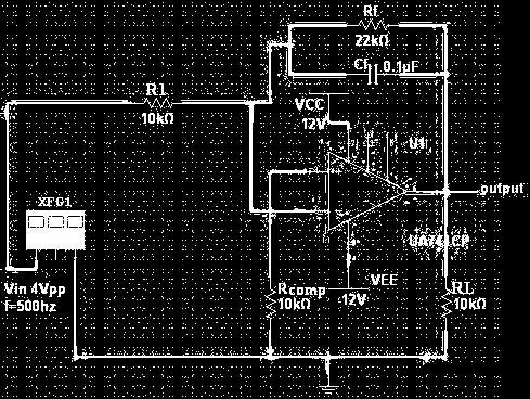
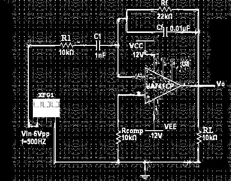
43 EXPERIMENT NO: 6 DATE SCHMITT TRIGGER CIRCUIT USING IC741 AIM: To study the Schmitt trigger characteristics by using IC741 and compare theoretical and practical values of the Upper Threshold voltage, V UT and the Lower Threshold voltage, V LT. APPARATUS: 741 Op-Amp Resistors Bread board Function generator CRO Probes Connecting wires THEORY: Circuit shows an inverting comparator with positive feedback. This circuit converts an irregular shaped waveform to square wave or pulse. This circuit is known as Schmitt trigger or Regenerative comparator or Squaring circuit. The input voltage V in triggers (changes the state of ) the output V o every time it exceeds certain voltage levels called Upper threshold voltage, V UT and Lower threshold voltage, V LT. The hysteresis width is the difference between these two threshold voltages i.e. V UT V LT. These threshold voltages are calculated as follows. V UT = (R 1 /R 1 +R 2 ) V sat when V o = V sat V LT = (R 1 /R 1 +R 2 ) (-V sat ) when V o = -V sat The output of Schmitt trigger is a square wave when the input is sine wave or triangular wave, where as if the input is a saw tooth wave then the output is a pulse wave. CIRCUIT DIAGRAM: PROCEDURE: 1. Connect the components/equipment as shown in the circuit diagram. 2. Switch ON the power supply. 37

44 3. Apply the input sine wave using function generator. 4. Connect the channel 1 of CRO at the input terminals and Channel-2 at the output terminals. 5. Observe the output square waveform corresponding to input sinusoidal signal. 6. Overlap both the input and output waves and note down voltages at positions on sine wave where output changes its state. These voltages denote the Upper threshold voltage and the Lower threshold voltage (see EXPECTED WAVEFORMS below). 7. Verify that these practical threshold voltages are almost same as the theoretical threshold voltages calculated using formulas given in the THEORY section above. 8. Sketch the waveforms by noting down the amplitude and the time period of the input V in and the output V o. EXPECTED WAVEFORMS: 38


45 TABLE: RESULT: QUESTIONS: 1. Which is type of comparator called Schmitt trigger using IC741? 2. What is the output wave of Schmitt trigger if the input is sine wave? 3. What type of waveform is obtained when triangular or ramp waveforms are applied to Schmitt trigger circuit? 4. Explain how a square wave is obtained at the output of timer when sine wave input is given? 5. What is the Threshold voltage? 6. How do you calculate the theoretical values of V UT and V LT in the case of IC741? 7. What is the Hysteresis width? 8. What is the minimum amplitude of the input sine wave in the case of Schmitt trigger using IC741? 39

46 IC Application and HDL simulation Lab Manual ECE,MRCET EXPERIMENT NO:7 DATE: IC565 PLL APPLICATIONS AIM: 1. To study the operation of NE565PLL 2.To use NE565 as multiplier EQUIPMENTSANDCOMPONENTS: APPARATUS: 1. DC power supply 1No. 2. CRO 1No. 3. Function Generator 1No. 4. Bread Board 1No. THEORY: The 565 is available as a14-pin DIP package. It is produced by Signatic Corporation. The output frequency of the VCO can be rewritten as f o = 0.25 / R T C T Hz. Where RT and CTare the external resistor and capacitor connected to pin8 and pin9. A value between 2k and 20k is recommended for RT.The VCO free running frequency is adjusted with RT and CT to be at the centre for the input frequency range. CIRCUIT DIAGRAM: 40
47 PROCEDURE: i. Connect the circuit using the component values as shown in the figure ii.measure the free running frequency of VCO at pin4 with the input signal Vinset= zero. Compare it with the calculated value=0.25/rtct iii. Now apply the input signal of 1Vpp square wave at a1khz to pin2 iv. Connect1 st channel of the scope to pin2 and display this signal on the scope. v.gradually increase the input frequency till the PLL is locked to the input frequency. This frequency f1 gives the lower ends of the capture range. Go on increase the input frequency; till PLL tracks the input signal, say to a frequency f2.this frequency f2 gives the upper end of the lock range. If the input frequency is increased further the loop will get unlocked. vi. Now gradually decrease the input frequency till the PLL is a gain locked. This is the frequency f3, the upper end of the capture range.keep on decreasing the input frequency until the loop is unlocked. This frequency f4 gives the lower end of the lock range vii. The lock range fl=(f2 f4) compare it with the calculated value of (7.8 f o /12) Also the capture range is fc=(f3 f1). Compare it with the calculated value of capture range. f c = [f L / (2)(3.6)(10 3 )C] 1/2 viii To use PLL as a multiplier,make connections as show in fig. The circuit uses a 4-bit binary counter7490 used as a divide-by-5circuit. ix. Set the input signal at 1Vpp square wave at 500Hz x.. Vary the VCO frequency by adjusting the 20K potentiometer till the PLL is locked. Measure the output frequency. xi. Repeat step9 and10 for input frequency of 1kHz and 1.5kHz. OBSERVATIONS: f O = f L = fc = CALCULATIONS: f L = (f 2 f 4 ) = 7.8f O /12 f C = (f 3 f 1 ) = [f L /(2) (3.6)(10 3 )C] 1/2 41

48 GRAPH: RESULT: f O = f L = f C = 42

49 EXPERIMENT No: 8 DATE VOLTAGE REGULATOR USING IC 723, THREE TERMINAL VOLTAGE REGULATORS 7805, 7809, 7912 AIM: To study the Fixed Voltage Regulators (1) 7805 (2) 7809 (3) 7812 (4) 7912 (5) 723 Variable Voltage Regulator THEORY: DC power for electronic circuits is most conveniently obtained from commercial ac lines by using rectifier - filter system, Called a dc power supply. The rectifier-filter combination constitutes an ordinary dc power supply. The dc voltage from an ordinary power supply remains constant so long as ac mains voltage or load is unaltered. However, in many electronic applications, it is desired that dc voltage should remain constant irrespective of changes in ac mains or load. Under such situations, voltage regulating devices are used with ordinary power supply. This constitutes regulated dc power supply and keeps the dc voltage at fairly constant value. ORDINARY DC POWER SUPPLY An ordinary or regulated dc power supply contains a rectifier and a filter circuit as shown in Fig-1. The output from the rectifier is pulsating dc. These pulsations are due to the presence of ac component in the rectifier output. The filter circuit removes the ac component so that steady dc voltage is obtained across the load. Limitations: An ordinary dc power supply has two following drawbacks: 1. The dc output voltage changes directly with input ac voltage. 2. The dc output voltage decreases as the load current increases. This is due to voltage drop in (a) Transformer windings (b) Rectifier (c) Filter circuit These variations in dc output voltage may cause inaccurate or erratic operation or even malfunctioning of many electronic circuits. Eg. In an oscillator, the frequency will shift and in transmitters, distorted output will result, therefore, ordinary power supply is unsuited for many applications and is being replaced by regulated power supply. For comparison of different types of power supplies, the following terms are commonly used: 43

50 1. Voltage Regulation : The dc voltage available across the output terminals of a given power supply depends upon load current. If the load current Idc is increased by decreasing RL as in Fig- 2, there is greater voltage drop in the power supply and hence smaller dc output voltage will be available. Reverse will happen if the load current decreases. The variation of output voltage w.r.t. the amount of load current drawn from the power supply is known as voltage regulation and is expressed by the following relation: % voltage regulation = (V NL - V FL ) / V FL * 100 V NL = dc output voltage at no load. V FL = dc output voltage at full load In a well designed power supply, the full load voltage is only slightly less than no -load voltage I.e. voltage regulation approaches zero. Therefore, lower the voltage regulation, the lesser the difference between full-load and no-load voltage and better is the power supply. Power supplies used in practice have a voltage regulation of 1% i.e. full load voltage is within 1% of the no -load voltage. Fig-3 shows the change of dc output voltage with load current. This is known as voltage regulation curve. 2. Minimum Load Resistance : The change of load connected to a power supply varies the load current and hence the dc output voltage. In order that a power supply gives the rated output voltage and current, there is minimum load resistance allowed. For instance, I a power supply is required to deliver a full-load current I FL at full load voltage V FL, then, Regulated Power Supply A dc power supply which maintains the output voltage constant irrespective of ac mains fluctuations or load variations is known as regulated dc power supply. A regulated power supply consists of an ordinary power supply and voltage regulating device an in fig-4. The output of ordinary power supply is fed to the voltage regulator which produces the final output. The output voltage (Vdc) remains constant whether the load current changes or there are fluctuations in the input ac voltage. 44


51 Need : In an ordinary power supply, the voltage regulation is poor i.e dc output voltage changes appreciably with load current. Moreover, output voltage also changes due to variations in the input ac voltage. This is due to the following reasons:- i) In practice, there are considerable variations in ac line voltage caused by outside factors beyond our control. This changes the dc output voltage. Most of the electronic circuits will refuse to work satisfactorily on such output voltage fluctuations. This necessitates to use regulated dc power supply. ii) The internal resistance of power supply is relatively large (>30W). Therefore, output voltage is markedly affected by the amount of load current drawn from the supply. These variations in dc voltage may cause erratic operation of electronic circuits. Therefore, regulated dc power supply is the only solution in such situations. HARDWARE SPECIFICATIONS: 1. Built - in 16V V / 350mA 12V V / 350mA 8V - 0-8V / 350mA AC sources 2. Bridge rectifier using IN4007 diodes - 1No. 3. Filter capacitors (470 F / 35V) - 2Nos. 4. Fixed Voltage Regulator No No No No. 5. Variable Voltage Regulator using 723 IC EXPERIMENTAL PROCEDURE: 45

52 1. Connect the circuit as shown in fig Connect different load resistors available in the front panel, note down the output current and voltage. 3. Also test the circuit with 12V V, 16V V AC sources also. 4. Remove 7805 and connect 7809, 7812 also repeat 2 and 3 steps. 5. Connect the circuit shown in fig Regulator It is a monolithic voltage regulator constructed on a single Silicon chip. The device consists of a temperature compensated reference amplifier,, error amplifier, power series pass transistor and current Limit circuitry. Additional NPN or PNP pass element may be used when output currents exceeding 150mA are required. Provisions are made for adjustable current limiting and remote shutdown. In addition to the above the device features low stand by current drain, low temperature drift and high Ripple rejections. The 723 is intended for use with positive or negative supplies as a series, shunt, switching or floating Regulator. Applications include laboratory power supplies, air borne systems and linear circuits. and other power supplies for digital CIRCUIT DESCRIPTION: Fig -4 shows the circuit of a variable regulator constructed with 723 IC. Pin is connected to positive terminal of the supply. 10KW potentiometer connected to pin 4, controls the output voltage. Output is available at Pin10. This output is not sufficient to drive loads. So it is passed through the Darlington pair of transistors (CL100). 46

 4. Measure the output voltage with a DMM and also measure the output with the 10KW potentiometer with its maximum position. 5.")


53 IC Application and HDL simulation lab Manual EXPERIMENTAL PROCEDURE: 1. Switch ON the experimental board by connecting power card to the AC mains. 2. Make sure that the potentiometer are in minimum position. 3. Connect the 8V AC tapping of the transformer secondary to the bridge rectifier input and short Raw DC +Ve point and pin 12 of 723 ( See Fig- ) 4. Measure the output voltage with a DMM and also measure the output with the 10KW potentiometer with its maximum position. 5. Now, disconnect the 8V AC tapping and connect 10V AC tapping and notedown the minimum and maximum output voltages with 10KW minimum and maximum positions. 6. Repeat the same procedure for 12V, 16V and 18V AC transformer secondary tapings and tabulate these values in Table Now, again connect 8V AC to the bridge rectifier input, set the output DC voltage at 5V with 10KW potentiometer. 8. Connect the load resistor with (0-50mA) milliammeter and vary the load resistor and note down the readings of the output voltage and output current with different load resistor. 9. Tabulate these values in Table-2. 47

/VFL * 100 11.")
54 LOAD REGULATION: 10. Calculate & Tabulate the load regulation at each load current. % Regulation = (VNL - VFL)/VFL * Draw a graph between load current Idc and load voltage V dc regulation. RESULT: 48
55 CYCLE - II 49


56 INTRODUCTION - XILINX Xilinx ISE is a software tool produced by Xilinx for synthesis and analysis of HDL designs, which enables the developer to synthesize ("compile") their designs, perform timing analysis, examine RTL diagrams, simulate a design's reaction to different stimuli, and configure the target device with the programmer. In our Lab, the scope is limited to design and analyze the design using test benches & simulation. The following is the step by step procedure to design in the Xilinx ISE: 1. New Project Creation Once the Xilinx ISE Design suite is started, open a new project & enter your design name and the location path. By default HDL is selected as the top-level source type. (If not, please select Top-level source type as HDL ) 50


57 2. Continue to the next window and check if the Preferred Language is selected as Verilog 3. Proceed by clicking Next and create a New Source using the Create New Source Window 51


58 4. Select the source type as Verilog Module and input a filename and proceed to Next. In the next window Define Module enter the ports. 5. Finish with the New project setup with the Summary window. 52


59 6. Once Finish is selected a pop-up appears to create the directory. Select yes 7. Then proceed to Next in the New Project Wizard to Add Existing Sources. Add source if an existing source is available, If not proceed to Next and finish with the Project Summary window 53

 within the")
60 8. Design Entry and Syntax Check The ports defined during the Project Creation are defined as a module in the filename.v file 9. Input your design (verilog code) within the module definition 54
 ready for implementation 11.")
61 10. Select the design from the Hierarchy window. In the below window of Processes Implement Design would be orange (in color) ready for implementation 11. Double click on implement design, it turns green (in color) once the design is implemented successfully and the Summary report is displayed. 55

62 12. Test-Bench creation, Simulation & Verification To add a test-bench to the existing design, right click on the.v file from the Hierarchy window and select New Source 13. Select Verilog Text Fixture from the Select Source Type and name the Test-Bench 56
63 14. Continue to Finish and a test bench is added in the project area 15. Edit the test bench as per your simulation requirements and select Behavioral Simulation in the Design Window. In the Processes window Isim Simulator would be displayed. First Proceed with the Behavioral Check Syntax 57


64 16. Double click on Behavioral Check Syntax & check for no errors 17. Then double click on Simulate Behavioral Model and the ISIM simulator window would open. Check for the outputs 58


 0 0 1 0 1 0 1 0 0 1 1 0 A B 0 0")
65 EXPERIMENT No: 1 DATE HDL CODE TO REALIZE ALL LOGIC GATES AIM: To develop the source code for logic gates by using VERILOG and obtain the simulation. SOFTWARE & HARDWARE: 1. XILINX 9.2i 2. FPGA-SPARTAN-3E LOGIC DIAGRAM: AND GATE: OR GATE: LOGIC DIAGRAM: TRUTH TABLE: LOGICDIAGRAM TRUTH TABLE: A B Y=AB A B Y=A+B NOT GATE: NAND GATE: LOGIC DIAGRAM: TRUTH TABLE: LOGICDIAGRAM TRUTH TABLE A B Y=(AB) A Y=A NOR GATE: XOR GATE: LOGIC DIAGRAM: TRUTH TABLE: LOGICDIAGRAM TRUTH TABLE: A B Y=(A+B) A B
; input a; input b; OUTPUT: [6:0] c; assign c[0]= a & b; assign c[1]= a b; assign")
![c[2]= ~(a & b); assign c[3]= ~(a b); assign c[4]= a ^ b; assign c[5]= ~(a ^ b); assign c[6]= ~ a; endmodule](/docs-images/87/96013270/images/66-2.jpg "SIMULATION OUTPUT: RESULT: Thus the OUTPUT s of all logic gates are verified by simulating the VERILOG code.")
66 IC Applications and HDL simulation Lab Manual XNOR GATE: LOGIC DIAGRAM: TRUTH TABLE: VERILOG SOURCE CODE: module logicgates1(a, b, c); input a; input b; OUTPUT: [6:0] c; assign c[0]= a & b; assign c[1]= a b; assign c[2]= ~(a & b); assign c[3]= ~(a b); assign c[4]= a ^ b; assign c[5]= ~(a ^ b); assign c[6]= ~ a; endmodule SIMULATION OUTPUT: RESULT: Thus the OUTPUT s of all logic gates are verified by simulating the VERILOG code. 60

; input a; input b; input en; output [3:0] z; reg [3:0] z; reg abar,bbar; always @")
67 EXPERIMENT No: 2 DATE DESIGN OF 2-TO-4 ENCODER AIM: To develop the source code for encoder by using VERILOG and obtain the simulation. SOFTWARE & HARDWARE: 1. XILINX 9.2i 2. FPGA-SPARTAN-3E DECODER LOGIC DIAGRAM: TRUTH TABLE: A B C Z(0) Z(1) Z(2) Z(3) VERILOG SOURCE CODE: module decoderbehv(a, b, en, z); input a; input b; input en; output [3:0] z; reg [3:0] z; reg abar,bbar; (a,b,en) begin z[0] = (abar&bbar&en); z[1] = (abar&b&en); z[2] = (a&bbar&en); z[3] = (a&b&en); end endmodule 61

68 SIMULATION OUTPUT: RESULT: Thus the OUTPUT s of encoder are verified by simulating the VERILOG code. 62

; input [7:0] d;")
69 EXPERIMENT No:3 DATE DESIGN OF 8-TO-3 ENCODER AIM: To develop the source code for encoder by using VERILOG and obtain the simulation. SOFTWARE & HARDWARE: 1. XILINX 9.2i 2. FPGA-SPARTAN-3E ENCODER: LOGIC DIAGRAM: TRUTH TABLE: D0 D1 D2 D3 D4 D5 D6 D7 X Y Z VERILOG SOURCE CODE: module encoderbehav(d, a,b,c); input [7:0] d; output x; output y; output z; reg a,b,c; (d [7:0]) begin a= d[4] d[5] d[6] d[7]; b= d[2] d[3] d[6] d[7]; c= d[1] d[3] d[5] d[7]; end endmodule 63

70 SIMULATION OUTPUT: RESULT: Thus the OUTPUT s of Encoded are verified by simulating the VERILOG code. 64

71 EXPERIMENT No: 4 DATE DESIGN OF 8-to-1MULTIPLEXER AND 1X8 DEMULTIPLEXER AIM: To develop the source code for 8x1 multiplexer and demultiplexer by using VERILOG and obtain the simulation. SOFTWARE & HARDWARE: 1. XILINX 9.2i 2. FPGA-SPARTAN-3E MULTIPLEXER: LOGIC DIAGRAM: 65
 begin")

72 TRUTH TABLE: VERILOG SOURCE CODE: module MUX8TO1(sel, A,B,C,D,E,F,G,H, MUX_OUT); input [2:0] sel; input A,B,C,D,E,F,G,H; output reg MUX_OUT; begin case(sel) 3'd0:MUX_OUT=A; 3'd1:MUX_OUT=B; 3'd2:MUX_OUT=C; 3'd3:MUX_OUT=D; 3'd4:MUX_OUT=E; 3'd5:MUX_OUT=F; 3'd6:MUX_OUT=G; 3'd7:MUX_OUT=H; default:; // indicates null endcase end endmodule 66


73 SIMULATION OUTPUT: DEMULTIPLEXER: LOGIC DIAGRAM: RESULT: Thus the OUTPUT s of Multiplexers and Demultiplexers are verified by simulating the VHDL and VERILOG code. 67

; input [3:0]")
74 EXPERIMENT No: 5 DATE DESIGN OF 4-BIT BINARY TO GRAY CONVERTER AIM: To develop the source code for binary to gray converter by using VERILOG and obtained the simulation. SOFTWARE & HARDWARE: 1. XILINX 9.2i 2. FPGA-SPARTAN-3E CODE CONVERTER (BCD TO GRAY): TRUTH TABLE: BCD GRAY LOGIC DIAGRAM: BEHAVIORAL MODELING: module b2g_behv(b, g); input [3:0] b; output [3:0] g; reg [3:0] g; 68
![always@(b) begin g[3]=b[3]; g[2]=b[3]^b[2]; g[1]=b[2]^b[1]; g[0]=b[1]^b[0]; end endmodule SIMULATION](/docs-images/87/96013270/images/75-1.jpg "OUTPUT: RESULT: Thus the OUTPUT s of binary to gray converter are verified by simulating the VERILOG")
75 begin g[3]=b[3]; g[2]=b[3]^b[2]; g[1]=b[2]^b[1]; g[0]=b[1]^b[0]; end endmodule SIMULATION OUTPUT: RESULT: Thus the OUTPUT s of binary to gray converter are verified by simulating the VERILOG code. 69
; output equal ; output greater ; output lower ; input [3:0] a ; input [3:0] b ;")
76 EXPERIMENT No: 6 DATE 4-BIT COMPARATOR AIM: To develop the source code for 4-Bit comparator by using VERILOG and obtained the simulation. SOFTWARE & HARDWARE: 1. XILINX 9.2i 2. FPGA-SPARTAN-3E 4-BIT COMPARATOR: LOGIC DIAGRAM: VERILOG SOURCE CODE: module comparator ( a,b,equal,greater,lower ); output equal ; output greater ; output lower ; input [3:0] a ; input [3:0] b ; (a or b) begin if (a<b) begin equal = 0; lower = 1; greater = 0; end else if (a==b) begin equal = 1; lower = 0; greater = 0; end else begin equal = 0; lower = 0; greater = 1; end end endmodule 70


77 SIMULATION OUTPUT: RESULT: Thus the OUTPUT s of 4-bit comparator is verified by simulating the VERILOG code. 71

78 EXPERIMENT No: 7 DATE DESIGN OF FULL ADDER USING THREE MODELING STYLES AIM: To develop the source code for full adder using three modeling styles by using VERILOG and obtained the simulation. SOFTWARE & HARDWARE: 1. XILINX 9.2i 2. FPGA-SPARTAN-3E FULL ADDER: LOGIC DIAGRAM: TRUTH TABLE: A B C SUM CARRY VERILOG SOURCE CODE: Dataflow Modeling: module fulladddataflow(a, b, c, sum, carry); input a; input b; input c; output sum; output carry; assign#2 p=a&b; assign#2 q=b&c; assign#2 r=c&a; assign#4 sum=a^b^c; assign#4carry =(p1 p2) p3; endmodule 72
79 Behavioral Modeling: module fuladbehavioral(a, b, c, sum, carry); input a; input b; input c; output sum; output carry; reg sum,carry; reg p1,p2,p3; (a or b or c) begin sum = (a^b)^c; p1=a & b; p2=b & c; p3=a & c; carry=(p1 p2) p3; end endmodule Structural Modeling: module fa_struct(a, b, c, sum, carry); input a; input b; input c; output sum; output carry; wire t1,t2,t3,s1 xor x1(t1a,b), x2(sum,s1,c); and a1(t1,a,b), a2(t2,b,c), a3(t3,a,c); or o1(carry,t1,t2,t3); endmodule 73

80 SIMULATION OUTPUT: RESULT: Thus the OUTPUT s of full adder using three modeling styles are verified by simulating the VERILOG code. 74

; input s; input r; input clk; input rst; output q; output qbar; reg q,qbar; always")
81 EXPERIMENT No: 8 DATE DESIGN OF FLIP FLOPS (SR,JK,D,T). AIM: To develop the source code for FLIP FLOPS by using VERILOG and obtained the simulation. SOFTWARE & HARDWARE: 1. XILINX 9.2i 2. FPGA-SPARTAN-3E SR FLIPFLOP: LOGIC DIAGRAM: TRUTH TABLE: Q(t) S R Q(t+1) X X VERILOG SOURCE CODE: Behavioral Modeling: module srflipflop(s, r, clk, rst, q, qbar); input s; input r; input clk; input rst; output q; output qbar; reg q,qbar; (posedge(clk) or posedge(rst)) begin if(rst==1'b1) begin q= 1'b0;qbar= 1'b1; end else if(s==1'b0 && r==1'b0) begin 75


 r==1'b0) JK")
 0 0 0 0 0 0 1 0 0 1 0 1 0 1 1 1")
82 ECE,MRCET q=q; qbar=qbar; end else if(s==1'b0 && begin q= 1'b0; qbar= 1'b1; end else if(s==1'b1 && begin q= 1'b1; qbar= 1'b0; end else begin q=1'bx;qbar=1'bx; end end endmodule SIMULATION OUTPUT: r==1'b1) r==1'b0) JK FLIPFLOP: LOGIC DIAGRAM: TRUTH TABLE: Q(t) J K Q(t+1)
83 VERILOG SOURCE CODE: Behavioral Modeling: module jkff(j, k, clk, rst, q, qbar); input j; input k; input clk; input rst; output q; output qbar; reg q; reg qbar; (posedge(clk) or posedge(rst)) begin if (rst==1'b1) begin q=1'b0; qbar=1'b1; end else if (j==1'b0 && k==1'b0) begin q=q; qbar=qbar; end else if (j==1'b0 && k==1'b1) begin q=1'b0; qbar=1'b1; end else if (j==1'b1 && k==1'b0) begin q=1'b1; qbar=1'b0; end else begin q=~q; qbar=~qbar; end end endmodule 77
 or posedge(rst)) begin if (rst==1'b1) begin q=1'b0; qbar=1'b1; end else if (d==1'b0) begin q=1'b0; qbar=1'b1;")
84 SIMULATION OUTPUT: D FLIPFLOP: LOGIC DIAGRAM: TRUTH TABLE: Q(t) D Q(t+1) VERILOG SOURCE CODE: Behavioral Modeling: module dff(d, clk, rst, q, qbar); input d; input clk; input rst; output q; output qbar; reg q; reg qbar; (posedge(clk) or posedge(rst)) begin if (rst==1'b1) begin q=1'b0; qbar=1'b1; end else if (d==1'b0) begin q=1'b0; qbar=1'b1; end 78


;")
85 else begin q=1'b1; qbar=1'b0; end end endmodule SIMULATION OUTPUT: T-FLIP FLOP LOGIC DIAGRAM: TRUTH TABALE: VERILOG SOURCE CODE: module t_flip_flop ( t,clk,reset,dout ); output dout ; input t ; input clk ; 79

86 wire clk ; input reset ; initial dout = 0; (posedge (clk)) begin if (reset) dout <= 0; else begin if (t) dout <= ~dout; end end endmodule SIMULATION OUTPUT: RESULT: Thus the OUTPUT s of Flip Flops are verified by simulating the VERILOG code. 80

![FPGA-SPARTAN-3E LOGIC DIAGRAM: VERILOG SOURCE CODE: module Counter_4Bit ( clk,reset,dout ); output [3:0] dout ; input](/docs-images/87/96013270/images/87-2.jpg "clk ; input reset ; initial dout = 0; always @ (posedge (clk)) begin if (reset) dout <= 0; else dout <= dout + 1; end")
87 EXPERIMENT-9 DATE DESIGN OF 4-BIT BINARY COUNTER AND BCD COUNTER AIM: To develop the source code for 4-bit binary counter and BCD counter by using VERILOG and obtained the simulation. SOFTWARE & HARDWARE: 1. XILINX 9.2i 2. FPGA-SPARTAN-3E LOGIC DIAGRAM: VERILOG SOURCE CODE: module Counter_4Bit ( clk,reset,dout ); output [3:0] dout ; input clk ; input reset ; initial dout = 0; (posedge (clk)) begin if (reset) dout <= 0; else dout <= dout + 1; end endmodule 81


![); output [3:0] dout ;;](/docs-images/87/96013270/images/88-3.jpg "input clk ; input reset ;")
88 SIMULATION OUTPUT: BCD COUNTER LOGIC DIAGRAM VERILOG SOURCE CODE module BCD_Counter ( clk,reset,dout ); output [3:0] dout ;; input clk ; input reset ; initial dout = 0 ; 82

89 (posedge (clk)) begin if (reset) dout <= 0; else if (dout<=9) begin dout <= dout + 1; end else if (dout==9) begin dout <= 0; end end endmodule SIMULATION OUTPUT: RESULT: Thus the OUTPUT s of 4-bit counter and BCD COUNTER using three modeling styles are verified by synthesizing and simulating the VERILOG code 83
Dev Bhoomi Institute Of Technology Department of Electronics and Communication Engineering PRACTICAL INSTRUCTION SHEET REV. NO. : REV.
 Dev Bhoomi Institute Of Technology Department of Electronics and Communication Engineering PRACTICAL INSTRUCTION SHEET LABORATORY MANUAL EXPERIMENT NO. ISSUE NO. : ISSUE DATE: July 200 REV. NO. : REV.
B.E. SEMESTER III (ELECTRICAL) SUBJECT CODE: X30902 Subject Name: Analog & Digital Electronics
 SUBJECT CODE: X30902 Subject Name: Analog & Digital Electronics") B.E. SEMESTER III (ELECTRICAL) SUBJECT CODE: X30902 Subject Name: Analog & Digital Electronics Sr. No. Date TITLE To From Marks Sign 1 To verify the application of op-amp as an Inverting Amplifier 2 To
B.E. SEMESTER III (ELECTRICAL) SUBJECT CODE: X30902 Subject Name: Analog & Digital Electronics Sr. No. Date TITLE To From Marks Sign 1 To verify the application of op-amp as an Inverting Amplifier 2 To
For input: Peak to peak amplitude of the input = volts. Time period for 1 full cycle = sec
 Inverting amplifier: [Closed Loop Configuration] Design: A CL = V o /V in = - R f / R in ; Assume R in = ; Gain = ; Circuit Diagram: RF +10V F.G ~ + Rin 2 3 7 IC741 + 4 6 v0-10v CRO Model Graph Inverting
INTEGRATED CIRCUITS AND APPLICATIONS LAB MANUAL
 INTEGRATED CIRCUITS AND APPLICATIONS LAB MANUAL V SEMESTER Department of Electronics and communication Engineering Government Engineering College, Dahod-389151 http://www.gecdahod.ac.in/ L A B M A N U
LIC & COMMUNICATION LAB MANUAL
 LIC & Communication Lab Manual LIC & COMMUNICATION LAB MANUAL FOR V SEMESTER B.E (E& ( E&C) (For private circulation only) NAME: DEPARTMENT OF ELECTRONICS & COMMUNICATION SRI SIDDHARTHA INSTITUTE OF TECHNOLOGY
MODEL ANSWER SUMMER 17 EXAMINATION Subject Title: Linear Integrated Circuit Subject Code:
 MODEL ANSWER SUMMER 17 EXAMINATION Subject Title: Linear Integrated Circuit Subject Code: Important Instructions to examiners: 1) The answers should be examined by key words and not as word-to-word as
Summer 2015 Examination
 Summer 2015 Examination Subject Code: 17445 Model Answer Important Instructions to examiners: 1) The answers should be examined by key words and not as word-to-word as given in the model answer scheme.
ASTABLE MULTIVIBRATOR
 555 TIMER ASTABLE MULTIIBRATOR MONOSTABLE MULTIIBRATOR 555 TIMER PHYSICS (LAB MANUAL) PHYSICS (LAB MANUAL) 555 TIMER Introduction The 555 timer is an integrated circuit (chip) implementing a variety of
Speed Control of DC Motor Using Phase-Locked Loop
 Speed Control of DC Motor Using Phase-Locked Loop Authors Shaunak Vyas Darshit Shah Affiliations B.Tech. Electrical, Nirma University, Ahmedabad E-mail shaunak_vyas1@yahoo.co.in darshit_shah1@yahoo.co.in
INTEGRATED CIRCULTS AND APPLICATIONS
 INTEGRATED CIRCULTS AND APPLICATIONS LAB MANUAL Subject Code : AEC106 Regulations : R16 Autonomous Class : V Semester (EEE) Prepared by Mrs. C DEEPTHI Assistant Professor Mr. MOHD.KHADIR Assistant Professor
Scheme I Sample Question Paper
 Sample Question Paper Marks : 70 Time: 3 Hrs. Q.1) Attempt any FIVE of the following. 10 Marks a) Classify configuration of differential amplifier. b) Draw equivalent circuit of an OPAMP c) Suggest and
LINEAR IC APPLICATIONS
 1 B.Tech III Year I Semester (R09) Regular & Supplementary Examinations December/January 2013/14 1 (a) Why is R e in an emitter-coupled differential amplifier replaced by a constant current source? (b)
CHAPTER 6 DIGITAL INSTRUMENTS
 CHAPTER 6 DIGITAL INSTRUMENTS 1 LECTURE CONTENTS 6.1 Logic Gates 6.2 Digital Instruments 6.3 Analog to Digital Converter 6.4 Electronic Counter 6.6 Digital Multimeters 2 6.1 Logic Gates 3 AND Gate The
Hours / 100 Marks Seat No.
 17445 21415 3 Hours / 100 Seat No. Instructions (1) All Questions are Compulsory. (2) Illustrate your answers with neat sketches wherever necessary. (3) Figures to the right indicate full marks. (4) Assume
AURORA S ENGINEERING COLLEGE BHONGIR, NALGONDA DIST
 AURORA S ENGINEERING COLLEGE BHONGIR, NALGONDA DIST. 508116. Lab manual of IC APPLICATIONS LAB 3 rd Year 1 st Sem. ECE 2014-15 DEPARTMENT OF ELECTRONICS AND COMMUNICATION ENGINEERING 1 PREFACE Integrated
An active filter offers the following advantages over a passive filter:
 ACTIVE FILTERS An electric filter is often a frequency-selective circuit that passes a specified band of frequencies and blocks or attenuates signals of frequencies outside this band. Filters may be classified
Government Polytechnic Muzaffarpur Name of the Lab: Applied Electronics Lab
 Government Polytechnic Muzaffarpur Name of the Lab: Applied Electronics Lab Subject Code: 1620408 Experiment-1 Aim: To obtain the characteristics of field effect transistor (FET). Theory: The Field Effect
LINEAR INTEGRATED CIRCUITS APPLICATIONS LABORATORY OBSERVATION
 LENDI INSTITUTE OF ENGINEERING AND TECHNOLOGY (Approved by A.I.C.T.E & Affiliated to JNTU, Kakinada) Jonnada (Village), Denkada (Mandal), Vizianagaram Dist 535005 Phone No. 08922-241111, 241112 E-Mail:
Multivibrators. Department of Electrical & Electronics Engineering, Amrita School of Engineering
 Multivibrators Multivibrators Multivibrator is an electronic circuit that generates square, rectangular, pulse waveforms. Also called as nonlinear oscillators or function generators. Multivibrator is basically
 RAJALAKSHMI ENGINEERING COLLEGE THANDALAM 602 105. DEPARTMENT OF ECE LAB MANUAL CLASS : II YEAR ECE SEMESTER : IV SEM (DEC 2009) SUBJECT CODE : EC2258 SUBJECT : LINEAR INTEGRATED CIRCUITS LAB PREPARED
COURSE DESCRIPTION (ELECTRICAL ENGINEERING LAB III (ECEg 2114)) COURSE OBJECTIVE: ASSESSMENT SCHEME AND TEACHING STRATEGY
) COURSE OBJECTIVE: ASSESSMENT SCHEME AND TEACHING STRATEGY") COURSE DESCRIPTION (ELECTRICAL ENGINEERING LAB III (ECEg 2114)) This course introduces the student to the Amplifier; Differential amplifier; Operational amplifier; Oscillators; Basic digital circuits Schmitt
COURSE DESCRIPTION (ELECTRICAL ENGINEERING LAB III (ECEg 2114)) This course introduces the student to the Amplifier; Differential amplifier; Operational amplifier; Oscillators; Basic digital circuits Schmitt
Question Paper Code: 21398
 Reg. No. : Question Paper Code: 21398 B.E./B.Tech. DEGREE EXAMINATION, MAY/JUNE 2013 Fourth Semester Electrical and Electronics Engineering EE2254 LINEAR INTEGRATED CIRCUITS AND APPLICATIONS (Regulation
SYLLABUS. osmania university CHAPTER - 1 : OPERATIONAL AMPLIFIER CHAPTER - 2 : OP-AMP APPLICATIONS ARATORS AND CONVERTERS
 Contents i SYLLABUS osmania university UNIT - I CHAPTER - 1 : OPERATIONAL AMPLIFIER Operational Amplifiers-Characteristics, Open Loop Voltage Gain, Output Impedance, Input Impedance, Common Mode Rejection
DEPARTMENT OF ELECTRICAL & ELECTRONICS ENGINEERING
 DEPARTMENT OF ELECTRICAL & ELECTRONICS ENGINEERING (Regulation 2013) EE 6311 LINEAR AND DIGITAL INTEGRATED CIRCUITS LAB MANUAL 1 SYLLABUS OBJECTIVES: Working Practice in simulators / CAD Tools / Experiment
DEPARTMENT OF ELECTRICAL ENGINEERING AND COMPUTER SCIENCE MASSACHUSETTS INSTITUTE OF TECHNOLOGY CAMBRIDGE, MASSACHUSETTS 02139
 DEPARTMENT OF ELECTRICAL ENGINEERING AND COMPUTER SCIENCE MASSACHUSETTS INSTITUTE OF TECHNOLOGY CAMBRIDGE, MASSACHUSETTS 019.101 Introductory Analog Electronics Laboratory Laboratory No. READING ASSIGNMENT
R (a) Explain characteristics and limitations of op-amp comparators. (b) Explain operation of free running Multivibrator using op-amp.
 Explain characteristics and limitations of op-amp comparators. (b) Explain operation of free running Multivibrator using op-amp.") Set No: 1 1. (a) Draw the equivalent circuits of emitter coupled differential amplifier from which calculate Ad. (b) Draw the block diagram of four stage cascaded amplifier. Explain the function of each
Set No: 1 1. (a) Draw the equivalent circuits of emitter coupled differential amplifier from which calculate Ad. (b) Draw the block diagram of four stage cascaded amplifier. Explain the function of each
Introduction to IC-555. Compiled By: Chanakya Bhatt EE, IT-NU
 Introduction to IC-555 Compiled By: Chanakya Bhatt EE, IT-NU Introduction SE/NE 555 is a Timer IC introduced by Signetics Corporation in 1970 s. It is basically a monolithic timing circuit that produces
Analog Electronic Circuits Lab-manual
 2014 Analog Electronic Circuits Lab-manual Prof. Dr Tahir Izhar University of Engineering & Technology LAHORE 1/09/2014 Contents Experiment-1:...4 Learning to use the multimeter for checking and indentifying
Power Line Carrier Communication
 IOSR Journal of Electronics and Communication Engineering (IOSR-JECE) e-issn: 2278-2834,p- ISSN: 2278-8735.Volume 9, Issue 2, Ver. II (Mar - Apr. 2014), PP 50-55 Power Line Carrier Communication Dorathe.
 VALLIAMMAI ENGINEERING COLLEGE SRM Nagar, Kattankulathur 603 203. DEPARTMENT OF ELECTRONICS & COMMUNICATION ENGINEERING QUESTION BANK SUBJECT : EC6404 LINEAR INTEGRATED CIRCUITS SEM / YEAR: IV / II year
EG572EX: ELECTRONIC CIRCUITS I 555 TIMERS
 EG572EX: ELECTRONIC CIRCUITS I 555 TIMERS Prepared By: Ajay Kumar Kadel, Kathmandu Engineering College 1) PIN DESCRIPTIONS Fig.1 555 timer Pin Configurations Pin 1 (Ground):- All voltages are measured
DEPARTMENT OF ELECTRICAL ENGINEERING AND COMPUTER SCIENCE MASSACHUSETTS INSTITUTE OF TECHNOLOGY CAMBRIDGE, MASSACHUSETTS 02139
 DEPARTMENT OF ELECTRICAL ENGINEERING AND COMPUTER SCIENCE MASSACHUSETTS INSTITUTE OF TECHNOLOGY CAMBRIDGE, MASSACHUSETTS 019 Spring Term 00.101 Introductory Analog Electronics Laboratory Laboratory No.
St.MARTIN S ENGINEERING COLLEGE
 St.MARTIN S ENGINEERING COLLEGE Dhulapally, Kompally, Secunderabad-500014. Branch Year&Sem Subject Name : Electrical and Electronics Engineering : III B. Tech I Semester : IC Applications OBJECTIVES QUESTION
EXPERIMENT 2.2 NON-LINEAR OP-AMP CIRCUITS
 2.16 EXPERIMENT 2.2 NONLINEAR OPAMP CIRCUITS 2.2.1 OBJECTIVE a. To study the operation of 741 opamp as comparator. b. To study the operation of active diode circuits (precisions circuits) using opamps,
1) Consider the circuit shown in figure below. Compute the output waveform for an input of 5kHz
 Consider the circuit shown in figure below. Compute the output waveform for an input of 5kHz") ) Consider the circuit shown in figure below. Compute the output waveform for an input of 5kHz Solution: a) Input is of constant amplitude of 2 V from 0 to 0. ms and 2 V from 0. ms to 0.2 ms. The output
) Consider the circuit shown in figure below. Compute the output waveform for an input of 5kHz Solution: a) Input is of constant amplitude of 2 V from 0 to 0. ms and 2 V from 0. ms to 0.2 ms. The output
EE 368 Electronics Lab. Experiment 10 Operational Amplifier Applications (2)
") EE 368 Electronics Lab Experiment 10 Operational Amplifier Applications (2) 1 Experiment 10 Operational Amplifier Applications (2) Objectives To gain experience with Operational Amplifier (Op-Amp). To
EE 368 Electronics Lab Experiment 10 Operational Amplifier Applications (2) 1 Experiment 10 Operational Amplifier Applications (2) Objectives To gain experience with Operational Amplifier (Op-Amp). To
The steeper the phase shift as a function of frequency φ(ω) the more stable the frequency of oscillation
 the more stable the frequency of oscillation") It should be noted that the frequency of oscillation ω o is determined by the phase characteristics of the feedback loop. the loop oscillates at the frequency for which the phase is zero The steeper the
It should be noted that the frequency of oscillation ω o is determined by the phase characteristics of the feedback loop. the loop oscillates at the frequency for which the phase is zero The steeper the
GOVERNMENT OF KARNATAKA KARNATAKA STATE PRE-UNIVERSITY EDUCATION EXAMINATION BOARD II YEAR PUC EXAMINATION MARCH-2013 SCHEME OF VALUATION
 GOVERNMENT OF KARNATAKA KARNATAKA STATE PRE-UNIVERSITY EDUCATION EXAMINATION BOARD II YEAR PUC EXAMINATION MARCH-03 SCHEME OF VALUATION Subject Code: 0 Subject: PART - A 0. What does the arrow mark indicate
SYLLABUS. osmania university UNIT - I UNIT - II UNIT - III CHAPTER - 4 : OPERATIONAL AMPLIFIER
 Contents i SYLLABUS osmania university UNIT - I CHAPTER - 1 : DIFFERENTIAL AMPLIFIERS Classification, DC and AC Analysis of Single/Dual Input Balanced and Unbalanced Output Configurations using BJTs. Level
Operational Amplifiers
 Operational Amplifiers Table of contents 1. Design 1.1. The Differential Amplifier 1.2. Level Shifter 1.3. Power Amplifier 2. Characteristics 3. The Opamp without NFB 4. Linear Amplifiers 4.1. The Non-Inverting
HIGH LOW Astable multivibrators HIGH LOW 1:1
 1. Multivibrators A multivibrator circuit oscillates between a HIGH state and a LOW state producing a continuous output. Astable multivibrators generally have an even 50% duty cycle, that is that 50% of
UNIT 2. Q.1) Describe the functioning of standard signal generator. Ans. Electronic Measurements & Instrumentation
 Describe the functioning of standard signal generator. Ans. Electronic Measurements & Instrumentation") UNIT 2 Q.1) Describe the functioning of standard signal generator Ans. STANDARD SIGNAL GENERATOR A standard signal generator produces known and controllable voltages. It is used as power source for the
UNIT 2 Q.1) Describe the functioning of standard signal generator Ans. STANDARD SIGNAL GENERATOR A standard signal generator produces known and controllable voltages. It is used as power source for the
About the Tutorial. Audience. Prerequisites. Copyright & Disclaimer. Linear Integrated Circuits Applications
 About the Tutorial Linear Integrated Circuits are solid state analog devices that can operate over a continuous range of input signals. Theoretically, they are characterized by an infinite number of operating
DMI COLLEGE OF ENGINEERING
 DMI COLLEGE OF ENGINEERING DEPARTMENT OF ELECTRONICS & COMMUNICATION ENGINEERING EC8453 - LINEAR INTEGRATED CIRCUITS Question Bank (II-ECE) UNIT I BASICS OF OPERATIONAL AMPLIFIERS PART A 1.Mention the
INSTITUTE OF AERONAUTICAL ENGINEERING (Autonomous) Dundigal, Hyderabad
 Dundigal, Hyderabad") 1 P a g e INSTITUTE OF AERONAUTICAL ENGINEERING (Autonomous) Dundigal, Hyderabad - 500 043 ELECTRONICS AND COMMUNICATION ENGINEERING TUTORIAL QUESTION BANK Name : INTEGRATED CIRCUITS APPLICATIONS Code
1 P a g e INSTITUTE OF AERONAUTICAL ENGINEERING (Autonomous) Dundigal, Hyderabad - 500 043 ELECTRONICS AND COMMUNICATION ENGINEERING TUTORIAL QUESTION BANK Name : INTEGRATED CIRCUITS APPLICATIONS Code
LAB MANUAL EC6412- LINEAR INTEGRATED CIRCUIT LABORATORY. Dharmapuri Regulation : 2013 Branch : B.E. ECE
 EC6412 LINEAR INTEGRATED CIRCUITS LABORATORY 1 Dharmapuri 636 703 LAB MANUAL Regulation : 2013 Branch Year & Semester : B.E. ECE : II Year / IV Semester EC6412- LINEAR INTEGRATED CIRCUIT LABORATORY EC6412
State the application of negative feedback and positive feedback (one in each case)
") (ISO/IEC - 700-005 Certified) Subject Code: 073 Model wer Page No: / N Important Instructions to examiners: ) The answers should be examined by key words and not as word-to-word as given in the model answer
(ISO/IEC - 700-005 Certified) Subject Code: 073 Model wer Page No: / N Important Instructions to examiners: ) The answers should be examined by key words and not as word-to-word as given in the model answer
UNIT I. Operational Amplifiers
 UNIT I Operational Amplifiers Operational Amplifier: The operational amplifier is a direct-coupled high gain amplifier. It is a versatile multi-terminal device that can be used to amplify dc as well as
Function Generator Using Op Amp Ic 741 Theory
 Function Generator Using Op Amp Ic 741 Theory Note: Op-Amps ua741, LM 301, LM311, LM 324 & AD 633 may be used To design an Inverting Amplifier for the given specifications using Op-Amp IC 741. THEORY:
Preface... iii. Chapter 1: Diodes and Circuits... 1
 Table of Contents Preface... iii Chapter 1: Diodes and Circuits... 1 1.1 Introduction... 1 1.2 Structure of an Atom... 2 1.3 Classification of Solid Materials on the Basis of Conductivity... 2 1.4 Atomic
DEPARTMENT OF ELECTRICAL ENGINEERING LAB WORK EE301 ELECTRONIC CIRCUITS
 DEPARTMENT OF ELECTRICAL ENGINEERING LAB WORK EE301 ELECTRONIC CIRCUITS EXPERIMENT : 4 TITLE : 555 TIMERS OUTCOME : Upon completion of this unit, the student should be able to: 1. gain experience with
GATE: Electronics MCQs (Practice Test 1 of 13)
") GATE: Electronics MCQs (Practice Test 1 of 13) 1. Removing bypass capacitor across the emitter leg resistor in a CE amplifier causes a. increase in current gain b. decrease in current gain c. increase
GATE: Electronics MCQs (Practice Test 1 of 13) 1. Removing bypass capacitor across the emitter leg resistor in a CE amplifier causes a. increase in current gain b. decrease in current gain c. increase
Gechstudentszone.wordpress.com
 8.1 Operational Amplifier (Op-Amp) UNIT 8: Operational Amplifier An operational amplifier ("op-amp") is a DC-coupled high-gain electronic voltage amplifier with a differential input and, usually, a single-ended
Difference between BJTs and FETs. Junction Field Effect Transistors (JFET)
") Difference between BJTs and FETs Transistors can be categorized according to their structure, and two of the more commonly known transistor structures, are the BJT and FET. The comparison between BJTs
Difference between BJTs and FETs Transistors can be categorized according to their structure, and two of the more commonly known transistor structures, are the BJT and FET. The comparison between BJTs
OPERATIONAL AMPLIFIER PREPARED BY, PROF. CHIRAG H. RAVAL ASSISTANT PROFESSOR NIRMA UNIVRSITY
 OPERATIONAL AMPLIFIER PREPARED BY, PROF. CHIRAG H. RAVAL ASSISTANT PROFESSOR NIRMA UNIVRSITY INTRODUCTION Op-Amp means Operational Amplifier. Operational stands for mathematical operation like addition,
R & D Electronics DIGITAL IC TRAINER. Model : DE-150. Feature: Object: Specification:
 DIGITAL IC TRAINER Model : DE-150 Object: To Study the Operation of Digital Logic ICs TTL and CMOS. To Study the All Gates, Flip-Flops, Counters etc. To Study the both the basic and advance digital electronics
Q1. Explain the Astable Operation of multivibrator using 555 Timer IC.
 Q1. Explain the Astable Operation of multivibrator using 555 Timer I. Answer: The following figure shows the 555 Timer connected for astable operation. A V PIN 8 PIN 7 B 5K PIN6 - S Q 5K PIN2 - Q PIN3
Phase-locked loop PIN CONFIGURATIONS
 NE/SE DESCRIPTION The NE/SE is a versatile, high guaranteed frequency phase-locked loop designed for operation up to 0MHz. As shown in the Block Diagram, the NE/SE consists of a VCO, limiter, phase comparator,
CHADALAWADA RAMANAMMA ENGINEERING COLLEGE (AUTONOMOUS) Chadalawada Nagar, Renigunta Road, Tirupati
 Chadalawada Nagar, Renigunta Road, Tirupati") IC APPLICATIONS LABORATORY MANUAL Subject Code : 15A04507 Regulations : R15 Class : V Semester (ECE) CHADALAWADA RAMANAMMA ENGINEERING COLLEGE (AUTONOMOUS) Chadalawada Nagar, Renigunta Road, Tirupati 517
IC APPLICATIONS LABORATORY MANUAL Subject Code : 15A04507 Regulations : R15 Class : V Semester (ECE) CHADALAWADA RAMANAMMA ENGINEERING COLLEGE (AUTONOMOUS) Chadalawada Nagar, Renigunta Road, Tirupati 517
GOVERNMENT OF KARNATAKA KARNATAKA STATE PRE-UNIVERSITY EDUCATION EXAMINATION BOARD II YEAR PUC EXAMINATION MARCH-2012 SCHEME OF VALUATION
 GOVERNMENT OF KARNATAKA KARNATAKA STATE PRE-UNIVERSITY EDUCATION EXAMINATION BOARD II YEAR PUC EXAMINATION MARCH-0 SCHEME OF VALUATION Subject Code: 0 Subject: Qn. PART - A 0. Which is the largest of three
Spectrum analyzer for frequency bands of 8-12, and MHz
 EE389 Electronic Design Lab Project Report, EE Dept, IIT Bombay, November 2006 Spectrum analyzer for frequency bands of 8-12, 12-16 and 16-20 MHz Group No. D-13 Paras Choudhary (03d07012)
DIGITAL COMMUNICATIONS LAB
 DIGITAL COMMUNICATIONS LAB List of Experiments: 1. PCM Generation and Detection. 2. Differential Pulse Code modulation. 3. Delta modulation. 4. Time Division Multiplexing of 2band Limited Signals. 5. Frequency
COMPARATOR CHARACTERISTICS The important characteristics of a comparator are these: 1. Speed of operation 2. Accuracy 3. Compatibility of output
 SCHMITT TRIGGER (regenerative comparator) Schmitt trigger is an inverting comparator with positive feedback. It converts an irregular-shaped waveform to a square wave or pulse, also called as squaring
SEM: V EXAM MARKS: 50 BRANCH: EC IA MARKS: 25 SUBJECT: ANALOG COMMUNICATION & LIC LAB SUB CODE: 06ECL58
 LIST OF EXPERIMENTS SEM: V EXAM MARKS: 50 BRANCH: EC IA MARKS: 25 SUBJECT: ANALOG COMMUNICATION & LIC LAB SUB CODE: 06ECL58 1) Active low pass & high pass filters second order 2) Active band pass & band
Dev Bhoomi Institute Of Technology Department of Electronics and Communication Engineering PRACTICAL INSTRUCTION SHEET
 Dev Bhoomi Institute Of Technology Department of Electronics and Communication Engineering PRACTICAL INSTRUCTION SHEET LABORATORY MANUAL EXPERIMENT NO. ISSUE NO. : ISSUE DATE: REV. NO. : REV. DATE : PAGE:
AC LAB ECE-D ecestudy.wordpress.com
 PART B EXPERIMENT NO: 1 AIM: PULSE AMPLITUDE MODULATION (PAM) & DEMODULATION DATE: To study Pulse Amplitude modulation and demodulation process with relevant waveforms. APPARATUS: 1. Pulse amplitude modulation
Department of Electronics & Telecommunication Engg. LAB MANUAL. B.Tech V Semester [ ] (Branch: ETE)
![Department of Electronics & Telecommunication Engg. LAB MANUAL. B.Tech V Semester [ ] (Branch: ETE)](/thumbs/86/93078052.jpg "Department of Electronics & Telecommunication Engg. LAB MANUAL. B.Tech V Semester [ ] (Branch: ETE)") Department of Electronics & Telecommunication Engg. LAB MANUAL SUBJECT:-DIGITAL COMMUNICATION SYSTEM [BTEC-501] B.Tech V Semester [2013-14] (Branch: ETE) KCT COLLEGE OF ENGG & TECH., FATEHGARH PUNJAB TECHNICAL
Department of Electronics & Telecommunication Engg. LAB MANUAL SUBJECT:-DIGITAL COMMUNICATION SYSTEM [BTEC-501] B.Tech V Semester [2013-14] (Branch: ETE) KCT COLLEGE OF ENGG & TECH., FATEHGARH PUNJAB TECHNICAL
LIC APPLICATIONS LAB MANUAL
 NRIIT/7.5.1/RC 08 NRI INSTITUTE OF TECHNOLOGY (Approved by AICTE, New Delhi :: Affiliated to JNTUK, Kakinada) POTHAVARAPPADU (V), (via) Nunna, Agiripalli (M), Krishna District, A.P. PIN : 521 212 Ph :
Facility of Engineering. Biomedical Engineering Department. Medical Electronic Lab BME (317) Post-lab Forms
 Post-lab Forms") Facility of Engineering Biomedical Engineering Department Medical Electronic Lab BME (317) Post-lab Forms Prepared by Eng.Hala Amari Spring 2014 Facility of Engineering Biomedical Engineering Department
Facility of Engineering Biomedical Engineering Department Medical Electronic Lab BME (317) Post-lab Forms Prepared by Eng.Hala Amari Spring 2014 Facility of Engineering Biomedical Engineering Department
the reactance of the capacitor, 1/2πfC, is equal to the resistance at a frequency of 4 to 5 khz.
 EXPERIMENT 12 INTRODUCTION TO PSPICE AND AC VOLTAGE DIVIDERS OBJECTIVE To gain familiarity with PSPICE, and to review in greater detail the ac voltage dividers studied in Experiment 14. PROCEDURE 1) Connect
Operating Manual Ver.1.1
 Multivibrators (Astable and Monostable) Operating Manual Ver.1.1 An ISO 9001 : 2000 company 94-101, Electronic Complex Pardesipura, Indore- 452010, India Tel : 91-731- 2570301/02, 4211100 Fax: 91-731-
Assignment 11. 1) Using the LM741 op-amp IC a circuit is designed as shown, then find the output waveform for an input of 5kHz
 Using the LM741 op-amp IC a circuit is designed as shown, then find the output waveform for an input of 5kHz") Assignment 11 1) Using the LM741 op-amp IC a circuit is designed as shown, then find the output waveform for an input of 5kHz Vo = 1 x R1Cf 0 Vin t dt, voltage output for the op amp integrator 0.1 m 1
Assignment 11 1) Using the LM741 op-amp IC a circuit is designed as shown, then find the output waveform for an input of 5kHz Vo = 1 x R1Cf 0 Vin t dt, voltage output for the op amp integrator 0.1 m 1
Department of Electronics & Communication Engineering LAB MANUAL SUBJECT: DIGITAL COMMUNICATION LABORATORY [ECE324] (Branch: ECE)
![Department of Electronics & Communication Engineering LAB MANUAL SUBJECT: DIGITAL COMMUNICATION LABORATORY [ECE324] (Branch: ECE)](/thumbs/96/127341232.jpg "Department of Electronics & Communication Engineering LAB MANUAL SUBJECT: DIGITAL COMMUNICATION LABORATORY [ECE324] (Branch: ECE)") Department of Electronics & Communication Engineering LAB MANUAL SUBJECT: DIGITAL COMMUNICATION LABORATORY [ECE324] B.Tech Year 3 rd, Semester - 5 th (Branch: ECE) Version: 01 st August 2018 The LNM Institute
Department of Electronics & Communication Engineering LAB MANUAL SUBJECT: DIGITAL COMMUNICATION LABORATORY [ECE324] B.Tech Year 3 rd, Semester - 5 th (Branch: ECE) Version: 01 st August 2018 The LNM Institute
Exam Booklet. Pulse Circuits
 Exam Booklet Pulse Circuits Pulse Circuits STUDY ASSIGNMENT This booklet contains two examinations for the six lessons entitled Pulse Circuits. The material is intended to provide the last training sought
Lecture 7 ECEN 4517/5517
 Lecture 7 ECEN 4517/5517 Experiments 4-5: inverter system Exp. 4: Step-up dc-dc converter (cascaded boost converters) Analog PWM and feedback controller to regulate HVDC Exp. 5: DC-AC inverter (H-bridge)
ME 365 EXPERIMENT 7 SIGNAL CONDITIONING AND LOADING
 ME 365 EXPERIMENT 7 SIGNAL CONDITIONING AND LOADING Objectives: To familiarize the student with the concepts of signal conditioning. At the end of the lab, the student should be able to: Understand the
CHAPTER 4: 555 TIMER. Dr. Wan Mahani Hafizah binti Wan Mahmud
 CHAPTE 4: 555 TIME Dr. Wan Mahani Hafizah binti Wan Mahmud 555 TIME Introduction Pin configuration Basic architecture and operation Astable Operation Monostable Operation Timer in Triggering Circuits 555
Document Name: Electronic Circuits Lab. Facebook: Twitter:
 Document Name: Electronic Circuits Lab www.vidyathiplus.in Facebook: www.facebook.com/vidyarthiplus Twitter: www.twitter.com/vidyarthiplus Copyright 2011-2015 Vidyarthiplus.in (VP Group) Page 1 CIRCUIT
 1 2 B.E./B.Tech. DEGREE EXAMINATION, NOVEMBER/DECEMBER 2010 Fourth Semester Electrical and Electronics Engineering EE 2254 LINEAR INTEGRATED CIRCUITS AND APPLICATIONS (Common to Instrumentation and Control
LESSON PLAN. SUBJECT: LINEAR IC S AND APPLICATION NO OF HOURS: 52 FACULTY NAME: Mr. Lokesh.L, Hema. B DEPT: ECE. Portions to be covered
 LESSON PLAN SUBJECT: LINEAR IC S AND APPLICATION SUB CODE: 15EC46 NO OF HOURS: 52 FACULTY NAME: Mr. Lokesh.L, Hema. B DEPT: ECE Class# Chapter title/reference literature Portions to be covered MODULE I
Experiment EB2: IC Multivibrator Circuits
 EEE1026 Electronics II: Experiment Instruction Learning Outcomes Experiment EB2: IC Multivibrator Circuits LO1: Explain the principles and operation of amplifiers and switching circuits LO2: Analyze high
DEPARTMENT OF E.C.E.
 PVP SIDDHARTHA INSTITUTE OF TECHNOLOGY, KANURU, VIJAYAWADA-7 DEPARTMENT OF E.C.E. ANALOG COMMUNICATIONS LAB MANUAL Department of Electronics & Communication engineering Prasad V.Potluri Siddhartha Institute
Tektronix Courseware. Academic Labs. Sample Labs from Popular Electrical and Electronics Engineering Curriculum
 Tektronix Courseware Academic Labs Sample Labs from Popular Electrical and Electronics Engineering Curriculum March 3, 2014 HalfWaveRectifier -- Overview OBJECTIVES After performing this lab exercise,
Fig 1: The symbol for a comparator
 INTRODUCTION A comparator is a device that compares two voltages or currents and switches its output to indicate which is larger. They are commonly used in devices such as They are commonly used in devices
CHAPTER 7 HARDWARE IMPLEMENTATION
 168 CHAPTER 7 HARDWARE IMPLEMENTATION 7.1 OVERVIEW In the previous chapters discussed about the design and simulation of Discrete controller for ZVS Buck, Interleaved Boost, Buck-Boost, Double Frequency
Transistor Design & Analysis (Inverter)
") Experiment No. 1: DIGITAL ELECTRONIC CIRCUIT Transistor Design & Analysis (Inverter) APPARATUS: Transistor Resistors Connecting Wires Bread Board Dc Power Supply THEORY: Digital electronics circuits operate
Experiment No. 1: DIGITAL ELECTRONIC CIRCUIT Transistor Design & Analysis (Inverter) APPARATUS: Transistor Resistors Connecting Wires Bread Board Dc Power Supply THEORY: Digital electronics circuits operate
FSK DEMODULATOR / TONE DECODER
 FSK DEMODULATOR / TONE DECODER GENERAL DESCRIPTION The is a monolithic phase-locked loop (PLL) system especially designed for data communications. It is particularly well suited for FSK modem applications,
 DHANALAKSHMI COLLEGE OF ENGINEERING MANIMANGALAM. TAMBARAM, CHENNAI B.E. ELECTRICAL AND ELECTRONICS ENGINEERING III SEMESTER EE6311 Linear and Digital Integrated Circuits Laboratory LABORATORY MANUAL CLASS:
6. HARDWARE PROTOTYPE AND EXPERIMENTAL RESULTS
 6. HARDWARE PROTOTYPE AND EXPERIMENTAL RESULTS Laboratory based hardware prototype is developed for the z-source inverter based conversion set up in line with control system designed, simulated and discussed
Facility of Engineering. Biomedical Engineering Department. Medical Electronic Lab BME (317) Pre-Report Forms
 Pre-Report Forms") Facility of Engineering Biomedical Engineering Department Medical Electronic Lab BME (317) Pre-Report Forms Prepared by Eng.Hala Amari Spring 2014 Facility of Engineering Biomedical Engineering Department
Facility of Engineering Biomedical Engineering Department Medical Electronic Lab BME (317) Pre-Report Forms Prepared by Eng.Hala Amari Spring 2014 Facility of Engineering Biomedical Engineering Department
EE 3101 ELECTRONICS I LABORATORY EXPERIMENT 9 LAB MANUAL APPLICATIONS OF IC BUILDING BLOCKS
 EE 3101 ELECTRONICS I LABORATORY EXPERIMENT 9 LAB MANUAL APPLICATIONS OF IC BUILDING BLOCKS OBJECTIVES In this experiment you will Explore the use of a popular IC chip and its applications. Become more
Analog Circuit II Laboratory ( EC 409) EC 409 Analog Electronics Lab - II
 EC 409 Analog Electronics Lab - II") Analog Circuit II Laboratory ( EC 409) Subject Subject Title L T P Contact Credit Full Code Hours / Unit# Marks EC 409 Analog Electronics Lab - II 0 0 2 2 1 100 Course Outcomes:- After successful completion
Analog Circuit II Laboratory ( EC 409) Subject Subject Title L T P Contact Credit Full Code Hours / Unit# Marks EC 409 Analog Electronics Lab - II 0 0 2 2 1 100 Course Outcomes:- After successful completion
INTEGRATED CIRCUITS. AN179 Circuit description of the NE Dec
 TEGRATED CIRCUITS AN79 99 Dec AN79 DESCPTION The NE564 contains the functional blocks shown in Figure. In addition to the normal PLL functions of phase comparator, CO, amplifier and low-pass filter, the
UNIT-V: WAVEFORM GENERATORS AND SPECIAL FUNCTION ICs. PARTA (2 Marks)
") UNIT-V: WAVEFORM GENERATORS AND SPECIAL FUNCTION ICs PARTA (2 Marks) 1. Define line regulation.[auc April 2004] It is defined as the percentage change in the output voltage from a change in the input voltage.
UNIT-V: WAVEFORM GENERATORS AND SPECIAL FUNCTION ICs PARTA (2 Marks) 1. Define line regulation.[auc April 2004] It is defined as the percentage change in the output voltage from a change in the input voltage.
Experiment 5.A. Basic Wireless Control. ECEN 2270 Electronics Design Laboratory 1
 .A Basic Wireless Control ECEN 2270 Electronics Design Laboratory 1 Procedures 5.A.0 5.A.1 5.A.2 5.A.3 5.A.4 5.A.5 5.A.6 Turn in your pre lab before doing anything else. Receiver design band pass filter
GATE SOLVED PAPER - IN
 YEAR 202 ONE MARK Q. The i-v characteristics of the diode in the circuit given below are : v -. A v 0.7 V i 500 07 $ = * 0 A, v < 0.7 V The current in the circuit is (A) 0 ma (C) 6.67 ma (B) 9.3 ma (D)
OBJECTIVE TYPE QUESTIONS
 OBJECTIVE TYPE QUESTIONS Q.1 The breakdown mechanism in a lightly doped p-n junction under reverse biased condition is called (A) avalanche breakdown. (B) zener breakdown. (C) breakdown by tunnelling.
Let us consider the following block diagram of a feedback amplifier with input voltage feedback fraction,, be positive i.e. in phase.
 P a g e 2 Contents 1) Oscillators 3 Sinusoidal Oscillators Phase Shift Oscillators 4 Wien Bridge Oscillators 4 Square Wave Generator 5 Triangular Wave Generator Using Square Wave Generator 6 Using Comparator
ELT 215 Operational Amplifiers (LECTURE) Chapter 5
 Chapter 5") CHAPTER 5 Nonlinear Signal Processing Circuits INTRODUCTION ELT 215 Operational Amplifiers (LECTURE) In this chapter, we shall present several nonlinear circuits using op-amps, which include those situations
CHAPTER 5 Nonlinear Signal Processing Circuits INTRODUCTION ELT 215 Operational Amplifiers (LECTURE) In this chapter, we shall present several nonlinear circuits using op-amps, which include those situations
Capacitive Touch Sensing Tone Generator. Corey Cleveland and Eric Ponce
 Capacitive Touch Sensing Tone Generator Corey Cleveland and Eric Ponce Table of Contents Introduction Capacitive Sensing Overview Reference Oscillator Capacitive Grid Phase Detector Signal Transformer