DEPARTMENT OF ELECTRONICS AND COMMUNICATION ENGINEERING POWER ELECTRONICS LABORATORY LAB MANUAL 10ECL VII SEMESTER
|
|
|
- Milo Atkins
- 5 years ago
- Views:
Transcription

1 APPROVED BY AICTE NEW DELHI, AFFILIATED TO VTU BELGAUM DEPARTMENT OF ELECTRONICS AND COMMUNICATION ENGINEERING & POWER ELECTRONICS LABORATORY LAB MANUAL 10ECL VII SEMESTER Prepared by: Reviewed by: Approved by: Sathisha B M Kavitha M V Dr. A.A. Powly Thomas Assistant professor Head of the Department Principal Dept. of ECE Dept. of ECE GCEM GCEM GCEM 81/1, 182/1, Hoodi Village, Sonnenahalli, K.R. Puram, Bengaluru, Karnataka
2 INDEX S.No Title Page No 1. Syllabus i 2. Course objective ii 3. Course outcome ii 4. Do s & Don t s iii 5. List of experiments iv 6. Viva questions 77
3 SYLLABUS POWER ELECTRONICS LAB Subject Code: 10ECL78 IA Marks: 25 No. of Practical Hrs/Week: 03 Exam Hours: 03 Total no. of Practical Hrs: 42 Exam Marks: Static characteristics of SCR and DIAC. 2. Static characteristics of MOSFET and IGBT. 3. Controlled HWR and FWR using RC triggering circuit 4. SCR turn off using i) LC circuit ii) Auxiliary Commutation 5. UJT firing circuit for HWR and FWR circuits. 6. Generation of firing signals for thyristors/ trials using digital circuits / microprocessor. 7. AC voltage controller using triac diac combination. 8. Single phase Fully Controlled Bridge Converter with R and R-L loads. 9. Voltage (Impulse) commutated chopper both constant frequency and variable frequency operations. 10. Speed control of a separately exited DC motor. 11. Speed control of universal motor. 12. Speed control of stepper motor. 13. Parallel / series inverter. Note: Experiments to be conducted with isolation transformer and low voltage. i
4 Course Objectives: To study and analyze V-I characteristics of SCR and DIAC. To study and analyze V-I characteristics of MOSFET and IGBT. To study and analyze various waveforms across different circuit elements in Full and Half wave rectifier using RC Firing circuit. To study and analyze various waveforms across different circuit elements in Full and Half wave rectifier using UJT Firing circuit. To study and analyze various waveforms across different circuit elements in Full and Half wave rectifier using Digital Firing circuit. To study and analyze various waveforms across different circuit elements various waveforms of AC voltage regulator using TRIAC and DIAC combination. To study and analyze Single phase Fully Controlled Bridge Converter with R and R-L loads. To study and analyze Voltage (Impulse) commutated chopper To study and analyze Speed control of a separately exited DC motor, Universal motor and stepper motor. To study and analyze various waveforms across different circuit elements in Parallel / series inverter Course Outcomes: The student will have the Ability: To conduct and analyze V-I characteristics of SCR and DIAC. To conduct and analyze V-I characteristics of MOSFET and IGBT To conduct and analyze Full and Half wave rectifier using RC Firing circuit To conduct and analyze Full and Half wave rectifier using UJT Firing circuit To conduct and analyze Full and Half wave rectifier using Digital Firing circuit. To conduct and analyze AC voltage regulator using TRIAC and DIAC combination To conduct and analyze Single phase Fully Controlled Bridge Converter with R and R-L loads To conduct and analyze Voltage (Impulse) commutated chopper To conduct and analyze Speed control of a separately exited DC motor, Universal motor and stepper motor. To conduct and analyze Parallel / series inverter. ii
5 DOS It is COMPULSORY to wear covered shoes when entering the lab. You must keep your bags at the designated area. Bags should NOT be placed on or under the workbench. Chairs and stools should be kept under the workbenches when not in use. Sit upright on chairs or stools, keeping feet on the floor. Follow the instructions of your lab demonstrator while conducting the experiments. In an emergency, all power in this lab can be switched off by pressing the button on the main breaker panel. It is to be used for emergencies ONLY DON TS Do NOT transfer equipment to other workbench or other labs without permission Do NOT touch any equipment until you are told to do so. Wearing a ring or watch can be hazardous in an electrical lab since such items make good electrodes for the human body NO food and drinks are allowed in this lab NEVER touch any equipments or components with wet or damp hands iii
6 List of Experiments Exp Experiment Nmae Page No No 1 Static characteristics of SCR and DIAC Static characteristics of MOSFET and IGBT Controlled HWR and FWR using RC triggering circuit UJT firing circuit for HWR and FWR circuits Generation of firing signals for thyristors/ trials using digital circuits / microprocessor. 6 AC voltage controller using triac diac combination SCR turn off using i) LC circuit ii) Auxiliary Commutation Single phase Fully Controlled Bridge Converter with R and R-L loads. 9 Speed control of a separately exited DC motor Speed control of universal motor Speed control of stepper motor Voltage (Impulse) commutated chopper both constant frequency and variable frequency operations Parallel / series inverter iv
7 Experiment No: 01 SCR AND DIAC CHARACTERISTICS Date: CHARACTERISTICS OF SCR: AIM: To plot the characteristics of an SCR and to find the forward resistance, holding current and latching current. APPARATUS: SCR & DIAC Characteristics Study unit. THEORY: A Silicon Controlled Rectifier (SCR) is a four layer, three terminals and three junction device, which is basically a rectifier with a control terminal called Gate. Like diode, it is also a uni-directional device and forward conduction is from anode to cathode. Since SCR use silicon for its construction so it is called silicon controlled rectifier. Where it operates as a rectifier, it is mainly used as a switch. There are three terminals namely Anode (A), Cathode (K), and Gate (G). Four layers, with alternatively P-type and N-type silicon semiconductors forming three junctions. If SCR is forward biased with G =0,the Junctions J1 and J3 are forward biased and J2 is reverse biased.if +V AK is small, leakage current flows (I FX ) until +V AK is large enough to cause reverse biased junction J2 to break down. The forward voltage at this point is called forward break over voltage V F (BR). If a negative voltage is applied to anode and a positive voltage is applied to cathode of the SCR, the junction J2 is forward biased and J1 and J2 are reverse biased with very small leakage current flow called reverse blocking current. If the reverse voltage is now increased, J1 and J3 break down in the zener or avalanche mode and I R is not limited, hence SCR could be damaged or destroyed. The region of the reverse characteristics before reverse breakdown is called reverse blocking region. CIRCUIT DIAGRAM: 1
8 PROCEDURE:- I. V I Characteristics: 1) Make the connections as given in the circuit diagram including meters. 2) Now switch ON the mains supply to the unit and initially keep V1 &V2 at minimum. 3) Set load potentiometer RL in the minimum position. 4) Adjust IG IG1 say 10 ma by varying VG or gate current potentiometer Rg. 5) Set load potentiometer Rg in the minimum position. Adjust IG IG1 say 10 ma by varying VG or gate current potentiometer RG. Slowly vary VL and note down V AK and IA readings for every 5 Volts and entered the readings in the tabular column. 6) Further vary VL till SCR conducts, this can be noticed by sudden drop of V AK and rise of IA readings. 7) Note down this readings and tabulated. Vary VL Further and note down IA and V AK readings. Draw the graph of V AK V/s I A. 8) The forward resistance or on state resistance can be calculated from the graph by using formula Tabular Column: Ron-State = ΔV AK /ΔI A Ω. I G = I G1 = ma I G = I G2 = ma V AK I A V AK I A II. To find latching current: 1) Apply about 20 V between Anode and Cathode by varying VA. Keep the load potentiometer RL at minimum position. The device must be in the OFF state with gate open. 2) Gradually increase Gate voltage - Vg till the device turns ON. This is the minimum gate current ( Ig min) required to turn ON the device. 3) Adjust the gate voltage to a slightly higher. Set the load potentiometer at the maximum resistance position. The device should comes to OFF state, otherwise decrease VA till the device comes to OFF state. 4) The gate voltage should be kept constant in this experiment. By varying RL, gradually increase load current IA in steps. Open and close the Gate voltage VG switch after each step. 5) If the anode current is greater the latching current of the device, the device stays on even after the gate switch is opened. Otherwise the device goes into blocking mode as soon as the gate switch is opened. 6) Note the latching current. Obtain the more accurate value of the latching current by taking small steps of IA near the latching current value. 2
9 III. To find Holding current: 1) Increase the load current from the latching current level by load pot RL or VL. 2) Open the gate switch permanently. The Thyristor must be fully ON. 3) Now start reducing the load current gradually by adjusting RL. 4) If the SCR does not turns OFF even after the RL at maximum position, then reduce VL. Observe when the device goes to Blocking mode. 5) The load current through the device at this instant, is the holding current of the device. Repeat the steps again to accurately get the I h. Normally I h < I l. Ideal graph of V-I characteristics of SCR + I A I h I L Ig2 Ig1 Ig0 VBO -V AK +V AK -I A RESULT: The values of VAK and IAK are noted down, graph is plotted and SCR forward resistance, Latching and Holding Currents are found. 3
10 CHARACTERISTICS OF DIAC: AIM: To study and plot the characteristics of an DIAC. APPARATUS: SCR & DIAC Characteristics Study unit. CIRCUIT DIAGRAM: - 20mA + - Rg I V + - V = 0-200V V1 PROCEDURE: 1) Make the connections as given in the circuit diagram. 2) Keep potentiometer also at minimum position. 3) Next switch ON the unit & VL power supply. 4) Vary VL insteps of 5V and note down the corresponding Ammeter reading. 5) Vary insteps of 5V up to 25Volts. After that vary insteps of 1V. 6) At a particular value of voltage the device conducts. This can be noticed by the sudden increase of Ammeter reading. 7) This is the device breakdown voltage, vary VL further and note down the corresponding V/I readings in the tabular column. 8) Reverse the supply to the DIAC and repeat the above procedure to find the reverse break down Voltage. Note :- If Voltage from V1 is not sufficient to turn on Diac, connect V1 and V2 supplies in series (connect V1- to V2 +)and use V1 + as + and V2 as. TABULAR COLUMAN V Volts I ma RESULT: The values of VAK and IAK are noted down, graph is plotted and SCR forward resistance, Latching and Holding Currents are found. 4
11 Experiment No: 02 Date: IGBT AND MOSFET CHARACTERISTICS AIM: To plot the static characteristics of MOSFET & IGBT. APPARATUS: IGBT & MOSFET Characteristics Study unit. Characteristics of MOSFET: THEORY: In n-channel depletion type MOSFET with gate positive with respect to source I D, V DS and V GS are drain current, drain source voltage and gate-source voltage. A plot of variation of I D with V DS for a given value of V GS gives the Drain characteristics or Output characteristics. If V GS & V DS are positive, I D is positive for n channel MOSFET and V GS is negative for depletion mode. V GS is positive for enhancement mode. MOSFET can be operated in three regions Cut-off region, Saturation region (pinch-off region) and Linear region. In the linear region I D varies linearly with V DS. i.e., increases with increase in V DS. Power MOSFETs are operated in the linear region for switching actions. In saturation region I D almost remains constant for any increase in V DS. Transfer characteristic gives the variation of I D with V GS for a given value of V DS. I D is the drain current with shorted gate. As curve extends on both sides V GS can be negative as well as positive. CIRCUIT DIAGRAM: 5
12 Trans Conductance Characteristics:- PROCEDURE: 1) Make the connections as shown in the circuit diagram with meters. 2) Initially keep V1 and V2 Minimum. Set V1= VDS1= say 10V.Slowly vary V2(VGS) and note down ID and VGS readings for every 0.5 Volts. and enter in the tabular column. 3) The minimum gate voltage VGS which is required for conduction to start in the MOSFET is called Threshold Voltage VGS(Th). 4) If VGS is less than VGS (Th) only very small leakage current flows from Drain to Source. If VGS is greater than VGS(Th), the Drain current depends on magnitude of the Gate Voltage. VGS varies from 2 to 5Volts. Repeat the same for different values of VDS and draw the graph of I D V/S VGS. TABULAR COLUMN:- V1= VDS1 = 10 Volts. V1 = VDS2 = 30 Volts V GS Volts ID ma VGS Volts ID ma IDEAL GRAPH : ID V DS = 15V VDS = 25V ID (on) V GS (Th) V GS (on) V GS 3.5V Drain Characteristics:- PROCEDURE: 1) Initially set V2 to VGS1= 3.5 Volts. 2) Slowly vary V1 and note down ID and VDS.For a Particular value of VGS1 there is a pinch off voltage ( Vp) between drain and source as Shown in figure. 3) If VDS is lower than Vp, the device works in the constant resistance region and ID is directly proportional to VDS. If VDS is more than Vp, constant ID flows from the device and this operating region is called constant current region. 4) Repeat the above for different values of VGS and note down ID V/S VDS 5) Draw the graph of I D V/S VDS for different values of VGS. 6
13 TABULAR COLUMN:- V2 = VGS = 3.5 Volts V2 = VGS=3.8 Volts VDS Volts ID ma VDS Volts ID ma IDEAL GRAPH : ID in ma V GS = 3.6V V GS = 3.55V V GS = 3.5V Characteristics of IGBT Theory: An output characteristic is a plot of collector current I C versus collector to emitter voltage V CE for given values of gate to emitter voltage V GE. A plot of collector current I C versus gate-emitter voltage V GE for a given value of V CE gives the transfer characteristic. Figure below shows the transfer characteristic. The Controlling parameter is the gate-emitter voltage V GE in IGBT. If V GE is less than the threshold voltage V T then IGBT is in OFF state. If V GE is greater than the threshold voltage V T then the IGBT is in ON state. IGBTs are used in medium power applications such as ac and dc motor drives, power supplies and solid state relays. CIRCUIT DIAGRAM: V DS 7
14 Transfer Characteristics:- PROCEDURE: 1) Make the connections as shown in the circuit diagram with meters. 2) Initially keep V1 and V2 minimum. Set V1= VCE1= say 10V.Slowly vary V2 (VGE) and note down IC and VGE readings for every 0.5 Volts. and enter in the tabular column. 3)The minimum gate voltage VGE which is required for conduction to start in the IGBT is called Threshold Voltage VGE(Th).If VGE is less than VGE (Th) only very small leakage current flows from Collector to Emitter. If VGE is greater than VGE(Th), the Collector current depends on magnitude of the Gate Voltage. VGE varies from 5 to 6Volts. 4) Repeat the same for different values of Vc and draw the graph of Ic V/S VGE. TABULAR COLUMN:- V1= VCE1 = Volts. V1 = VCE2 = ----Volts V GE Volts ID ma VGE Volts ID ma 8
15 IDEAL GRAPH : IC V CE = 15V VCE = 25V IC (on) V GE (Th) V GE (on) V GE Collector Characteristics:- PROCEDURE: 1) Initially set V2 to VGE1= 5 Volts. Slowly vary V1 and not down IC and VGE. For a Particular value of VGE1 there is a pinch off voltage ( Vp) between Collector and Emitter as Shown in figure. 2) If VGE is lower than Vp, the device works in the constant resistance region and IC is directly proportional to VGE. If VGE is more than Vp, constant IC flows from the device and this operating region is called constant current region. 3) Repeat the above for different values of VGE and note down IC values. 4) Draw the graph of I C V/S V GE for different values of V GE. TABULAR COLUMN:- V2 = VGE = 5.0 Volts V2 = VGE=5.2Volts VCE Volts IC ma VCE Volts IC ma 9
16 IDEAL GRAPH : IC in V GE = 5.25V ma V GE = 5.2V V GE = 5.15V V GE = 5.1V RESULT: The transfer characteristics & collector characteristics are obtained and their respective graphs are plotted and output resistance and Trans conductance are found. V CE 10
17 Experiment No: 03 Date: RC HALF AND FULL WAVE FIRING CIRCUIT AIM: To study the static characteristics of RC Half and Full wave firing circuit. APPARATUS: RC Firing circuit Study unit THEORY: In the negative half cycle of the AC supply, diode D 2 is forward biased. It will short circuit the potentiometer R and the capacitor C is charged to negative peak voltage through D 2 as shown in fig (a). with its upper plate negative with respect to its lower plate. In the positive half cycle, D 2 is reverse biased. The capacitor C will charged through R to the trigger point of the thyristor in a time determined by the RC time constant and the rising anode voltage(see fig(b)). The diode D 1 will isolate and protect the gate cathode junction against reverse (negative) voltage. As soon as the capacitor voltage become sufficiently positive to forward bias. Diode D 1 and the gate cathode junction of thyristor will be turned on. As soon as the thyristor is turned on, the voltage across it reduced to a very low value and the gate current goes to zero. R-C HALF WAVE FIRING CIRCUIT: Circuit diagram : 11
18 Connection Diagram for RC Half wave Firing Circuit : PROCEDURE: 1) Make the connections as given in the circuit diagram. 2) Connect a Resistance of 50 ohms between the load points. 3) Vary the control pot(r) and observe the voltage waveforms across load, SCR and at different points of the circuit. 4) Note down the output voltage across the Load for different values of firing angle in degree. 5) Calculate the theoretical and practical output voltage. 6) Draw the graph for input wave form, output waveforms across SCR and Load. TABULAR COLUMN: Sl no. Firing Angle Load Voltage Theoretical [Vm/2 ( 1 +cos ) In Volts Practical in Volts 12


19 VARIOUS WAVEFORMS FOR RC HALF WAVE CONTROL Wave forms across Input and load: Vin Vload Wave forms across Load and SCR: Vscr Vload Firing Angle = X/Y
20 RC FULL WAVE FIRING CIRCUIT Circuit diagram: Connection Diagram for RC Full wave Firing 14
 Vary the pot and observe the voltage waveforms across load, SCR and at different points of the circuit.")
 Draw the graph for input wave form, output waveforms across SCR and Load.")
21 PROCEDURE : 1) Make the connections as given in the circuit diagram. 2) Connect a Rheostat of 100 ohms between the load points. 3) Vary the pot and observe the voltage waveforms across load, SCR and at different points of the circuit. 4) Note down the output voltage across the Load for different values of firing angle in degree. 5) Calculate the theoretical and practical output voltage. 6) Draw the graph for input wave form, output waveforms across SCR and Load. VARIOUS WAVEFORMS FOR RC FULL WAVE CONTROL: Wave forms across Input and load: Vin Vload Wave forms across Load and SCR: Vscr Vload RESULT:- Half and full wave R & RC triggering circuit have been rigged up and output waveforms have been plotted. 15
22 Experiment No: 04 Date: HALF AND FULL WAVE RECTIFIER USING UJT FIRING CIRCUIT AIM: To study the static characteristics of RC Half and Full wave firing circuit. APPARATUS: UJT Firing circuit Study unit Theory: UJT is highly efficient switch. The switching time is in the range of nanoseconds. Since UJT exhibits negative resistance characteristics it can be used as relaxation oscillator. The circuit diagram is as shown with R 1 and R 2 being small compared to R B1 and R B 2 of UJT. When V BB is applied, capacitor C begins to charge through resistor R exponentially towards V BB. During this charging emitter circuit of UJT is an open circuit. The rate of charging is 1 RC. When this capacitor voltage, which is nothing but emitter voltage, V E reaches the peak pointv P V BB V D, the emitter base junction is forward biased and UJT turns on. Capacitor C rapidly discharges through load resistance R 1 with time constant 2 R 1 C. When emitter voltage decreases to valley point V v, UJT turns off. Once again the capacitor will charge towards V BB and the cycle continues. The resistor R in the circuit will determine the rate of charging of the capacitor. If R is small the capacitor charges faster towards V BB and thus reaches V P faster and the SCR is triggered at a smaller firing angle. If R is large the capacitor takes a longer time to charge towards V P the firing angle is delayed. Circuit Diagrams:- Single phase Half wave Rectifier: 20 T1 230V AC Supply 0 R Load 50Ω/25Watt 20 Single phase Full wave Rectifier:- T V AC Supply 0 R- Load 50Ω/25Watt 20 T2 16
23 PROCEDURE: I. Firing of SCR using UJT for half wave rectifier:- 1) Switch ON the mains supply observe and note down the wave forms at the different points in the circuit and also the trigger O/ps T1, & T1. 2) Make sure that the pulse transformer O/ps T1 & T1 are proper and synchronized. 3) Now make the connections as given the circuit diagram for Half wave rectifier using AC source,ujt relaxation Oscillator, SCR(T1)and a suitable load (50Ohms/25wattResistor) 4) Now switch ON the mains supply, observe and note down the output waveforms across load And SCR. 5) Draw the wave forms at different firing angle 120, 90 & 60 for both Half & full wave rectifier 6) In the UJT firing Circuit the firing angle can be varied from 150degree to 30degree approximately. 7) We cannot vary from exact 0degree to 180degree as we vary in single phase converter firing circuit. 8) This is one of the simplest method of SCR triggering. 9) We can also fire SCR s in the different Power circuits like Single phase half controlled converter, Single phase AC voltage controller using both SCR and Triac. II. Firing of SCR using UJT for Full wave rectifier:- 1) Switch ON the mains supply observe and note down the wave forms at the different points in the circuit and also the trigger O/ps T1, & T1. 2) Make sure that the pulse transformer O/ps T1 & T1 are proper and synchronized. Now make the connections as given the circuit diagram for Fullwave rectifier using ACsource, UJT relaxationoscillator, SCR s(t1andt2)and a suitable load(50ohms/25wattresistor) 3) Now switch ON the mains supply, observe and note down the output waveforms across load And SCR. 4) Draw the wave forms at different firing angle 120, 90 & 60 for both Half & full wave rectifier 5) In the UJT firing Circuit the firing angle can be varied from 150degree to 30degree approximately. 6) We cannot vary from exact 0degree to 180degree as we vary in single phase converter firing circuit. 7) This is one of the simplest method of SCR triggering. 8) We can also fire SCR s in the different Power circuits like Single phase half controlled converter,singl phase AC voltage controller using both SCR and Triac. a. UJT Relaxation Oscillator: 1) To Study oscillator using UJT, short CF to the diode bridge rectifier to get filtered DC output. 2) Now we will get the equidistant pulses at the o/p of pulse transformer. 3) The frequency of the pulses can be varied by varying the potentiometer RC. 4) Draw the wave forms at different points by varying RC. Firing Angle = X/Y
24 Connection Diagram for Half wave rectifier using UJT Firing Circuit T1 R C T1 AC DZ C EMITTER B1 B2 R Load C F T2 T2 MAINS 20VAC 0V 20VAC Table1:- Synchronized UJT triggering circuit for HWR:- Sl no. Firing Angle Load Voltage Theoretical [Vm/2 ( 1 +cos ) In Volts Practical in Volts 18

")
25 VARIOUS WAVEFORMS FOR UJT HALF WAVE RECTIFIER Vin Vload Wave forms across Input and load Vload Vscr Wave forms across Load and SCR (maximum α) Vload Vscr Wave forms across Load and SCR (minimum α) 19

26 Connection Diagram for Full wave rectifier using UJT VARIOUS WAVEFORMS FOR UJT FULL WAVE RECTIFIER Vload Vscr Wave forms across Load and SCR 20
27 Table 2; Synchronized UJT triggering circuit for FWR:- Sl no. Firing Angle Load Voltage Theoretical [Vm/ ( 1 +cos ) In Volts Practical in Volts NOTE:- a) At lower firing angles SCR may not turn on due to the fact that UJT takes some time (charging time) to generate first firing pulse. b)at higher firing angles SCR may not turn on due to the fact that VAK is insufficient to turn-on SCR. RESULT:- UJT Relaxation oscillator and UJT HALF & FULL WAVE CONTROLLED CIRCUITS is constructed and its performance is studied. 21
28 Experiment No: 05 Date: HALF AND FULL WAVE DIGITAL FIRING CIRCUIT AIM: To study the static characteristics of Half and Full wave Digital firing circuit. APPARATUS: Digital Firing circuit Study unit BLOCK DIAGRAM OF THE DIGITAL FIRING CIRCUIT. R Preset ( N no. of counting bits) N bit _ Fixed Freq. Counter-3 Logic ckt. + Fixed freq. Clock N bit max Flip Flop B Modulator Logic ckt hjtptptp Oscillator (ff.) stage Flip Flop min S monostable (F/F) En oscillator + driver stage R Reset Reset Load A A _ Fc TM TA Sync. Signal (~ 10V) DC 5V Supply ZCD _ C Carrier Frequency Oscillator. (~ 5 khz) A _ A 22


29 Different waveforms for Digital firing unit AC REF ZCD RESET CLK COUNTER O/P CLOCK GEN. O/P f C oscillator output 23

30 O/P T P O/P T N O/P T M O/P TA TRIGGER OUTPUTS T 1 &T 1 T 2 &T 2 24
31 PROCEDURE FOR TRIGGERING OF SCR :- 1. Firing of SCR(Half wave converter) using digital firing circuit :-. 10) Switch ON the mains supply observe and note down the wave forms at the different points In the circuit. 11) Connect Tp and Tn o/ps to 1 and 2 input of pulse transformer isolation circuit. 12) Make sure that the pulse transformer outputs are proper and synchronized. 13) We will get the pulse transformer isolated trigger o/ps at T1, T1 1, T2 and T2 1, connect the trigger o/p T1 or T2 to Gate and Cathode of SCR. 14) Now make the connections as given the circuit diagram for Half wave rectifier using AC source, Digital firing circuit, SCR and a load (100 Ohms/25watt) supplied along with this unit. 15) Select 180 / 100% selector switch to 180* mode(converter expt. Mode). 16) Now switch ON the mains supply, observe and note down the output waveforms across load And SCR by varying firing angle in steps of 10degrees. 17) Draw the wave forms at different firing angle 120, 90, 60,30,0 degrees for half wave rectifier 18) In the firing Circuit the firing angle can be varied from 180degree to 0 degrees. 19) This is one of the triggering method of SCR. 20) We can also fire SCR s in the different Power circuits like Single phase half controlled converter,single phase AC voltage controller using both SCR, and Triac.. CIRCUIT DIAGRAM:- Single phase Half wave Rectifier: 20 T1 R Load 100Ω/25Watt 0 NOTE: - If there is no output even after all the proper connections, switch OFF the Supply and interchange the connections at step down transformer terminals. This is to make the power circuit and firing to synchronize. 25
 using digital firing circuit :-. 1) Switch ON the mains supply observe and note down the wave forms at the different points In the circuit.")
 We will get the pulse transformer isolated trigger o/ps at T 1, T 1 1, T 2 and T 2 1, connect the trigger o/p T 1 or T 2 to Gate and Cathode of SCR.")
32 VARIOUS WAVEFORMS FOR SINGLE PHASE HALF WAVE RECTIFIER Wave forms across Input and load (α=90 ) Vin V load Wave forms across Load and SCR (α=90 ) V load V scr PROCEDURE FOR TRIGGERING OF SCR :- 2. Firing of SCR(Full wave converter) using digital firing circuit :-. 1) Switch ON the mains supply observe and note down the wave forms at the different points In the circuit. 2) Connect T p and T n o/ps to 1 and 2 input of pulse transformer isolation circuit. 3) Make sure that the pulse transformer outputs are proper and synchronized. 4) We will get the pulse transformer isolated trigger o/ps at T 1, T 1 1, T 2 and T 2 1, connect the trigger o/p T 1 or T 2 to Gate and Cathode of SCR. 5) Now make the connections as given the circuit diagram for full wave rectifier using AC source, Digital firing circuit, SCRs and a load (100 Ohms/25watt) supplied along with this unit. 6) Select 180 / 100% selector switch to 180* mode(converter expt. Mode). 26
 Draw the wave forms at different firing angle 120, 90, 60,30,0 degrees for full wave rectifier 9) In the firing Circuit the firing angle can be varied from 180degree to 0 degrees.")
33 7) Now switch ON the mains supply, observe and note down the output waveforms across load And SCR by varying firing angle in steps of 10degrees. 8) Draw the wave forms at different firing angle 120, 90, 60,30,0 degrees for full wave rectifier 9) In the firing Circuit the firing angle can be varied from 180degree to 0 degrees. 10) This is one of the triggering method of SCR. 11) We can also fire SCR s in the different Power circuits like Single phase half controlled converter,single phase AC voltage controller using both SCR, and Triac.. CIRCUIT DIAGRAM:- Single phase Full wave Rectifier:- T R- Load 100Ω/25Watt 20 T 2 NOTE: - If there is no output even after all the proper connections, switch OFF the Supply and interchange the connections at step down transformer terminals. This is to make the power circuit and firing to synchronize. VARIOUS WAVEFORMS FOR SINGLE PHASE FULL WAVE RECTIFIER Wave forms across Input and load (α=90 ) Vin Vload 27

34 Wave forms across SCR1(T 1 ) and SCR2(T 2 ) (α=90 ) V T1 V T2 RESULT:- Half and full wave Digital triggering circuit have been rigged up and output waveforms have been plotted. 28
35 Experiment No: 06 Date: AC VOLTAGE CONTROLLER USING TRIAC-DIAC AIM: To study the static characteristics of RC Half and Full wave firing circuit. APPARATUS: Light Dimmer circuit Study unit THEORY: AC VOLTAGE CONTROLLERS If a Thyristor switch is connected between AC supply and load, the power flow can be controlled by varying the rms value of AC voltage applied to the load, and this type of power circuit is known as an AC voltage controller. The most common application of AC voltage controller are; Industrial heating, onload transformer tap changing, light controls, speed control of polyphase induction motors and AC magnet controls. For power transfer, two types of control are normally used : 1. On Off control 2. Phase angle control In On Off control, thyristor switches connect the load to the AC source for a few cycles of input voltage and then disconnect it for another few cycles. This is trivial in nature and will not be discussed here. In Phase control, thyristor switches connect the load to the AC source for a portion of each type of input voltage. This mode of control will be the subject of discussion in this section. Since the input voltage is AC, thyristors are line commutated; and phase control thyristors, (converter grade thyristors), which are relatively inexpensive and slower than fast switching thyristors, are normally used. For applications upto 400Hz, if TRIAC s are available to meet the voltage and current ratings of a particular application, TRIAC s are more commonly used. Circuit diagram: LAMP MT 2 R V AC 47K V R1 R Diac (DB3) Gate TRIAC 0.1 F C 1 C F MT 1 29
 Switch ON the mains supply, vary the firing angle potentiometer and observe the variation in lamp brightness and also note down the voltage variation across the lamp.")
36 Connection diagram: PROCEDURE: 1) Make the connections as given in the circuit diagram. 2) Connect the lamp at load terminals. 3) Switch ON the mains supply, vary the firing angle potentiometer and observe the variation in lamp brightness and also note down the voltage variation across the lamp. 4) Observe the waveform across the lamp and Triac. Different waveforms for AC voltage controller using triac-diac Vin Vload Voltage waveforms across input and load(lamp) 30

37 Vload Vtriac Voltage waveforms across Load(lamp) and Device(Triac) Firing Angle α = X/Y 180 TABULAR COLUMN For Lamp Load:- Sl. No. Input Voltage AC in volts V 50V 50V.... Firing angle In Degrees Output voltage AC in Volts RESULT:-AC voltage controller using TRIAC and DIAC have been rigged up and output waveforms have been plotted. 31
38 Experiment No: 07 SCR TURN OFF METHODS Date: AIM: To study the commutation circuit Using LC circuit and Auxillary Commutation. APPARATUS: Forced commutation circuit Study unit THEORY: CLASS B COMMUTATION: (Self Commutation by an LC circuit):- In this type of commutation reverse voltage is applied to the thyristor by the over swinging of an Under damped LC circuit connected across the Thyristor. Capacitor charges up to the supply voltage before the trigger pulse is applied to the gate. When the thyristor is triggered, two currents flow, a load current through the external circuit and a pulse of current through LC circuit and thyristor in opposite direction. This resonant current tends to turn off the thyristor. CIRCUIT DIAGRAM: L T 1 C 24v R PROCEDURE: - 1)Make the interconnections as shown in the circuit diagram, connect trigger output T1 to Gate and cathode of SCR T1. 2)Switch on the DC supply to the power circuit and observe the voltage wave forms across load by varying the frequency, potentiometer. Duty cycle potentiometer is of no use in this experiment. 3)Repeat the same for different values of L, C and R 32


39 DIFFERENT WAVEFORMS FOR CLASS B COMMUTATION Vscr V load V load V C 33
40 CLASS D COMMUTATION: (Auxilliary Commutation by an LC circuit):- This type of commutation is popular due to the design flexibility. There are many choppers and Inverters under this class.t2 must be triggered first in order to charge up capacitor C is charged, T2 is commutated off owing to lack of current. When T1 is triggered, current flows in two paths, load current through R L and Commutating current through C T1, L and D1. The charge on the capacitor is reversed and held with The hold off diode D1. At any desired instant T2 may be triggered when then Places C across T1 via T2 and T1 is turned off. CIRCUIT DIAGRAM: PROCEDURE: 1) Make the connections as given in the circuit diagram. 2) Connect T1 and T2 gate pulse from the firing circuit to the corresponding SCRs in the power circuit. Initially keep the Trigger ON/OFF at OFF position to initially charge the capacitor, this can be observed by connecting CRO across the Capacitor. 3) Now Switch ON the trigger O/P switch and observe the Voltage wave forms across the load, T1, T2 and Capacitor. 4) Note down the voltage waveforms Across the load, T1, T2 and capacitor. 5) Note down the voltage waveforms at different frequency of chopping and also at different duty cycle. 6) Repeat the experiment for different values of load resistance, commutation inductance and capacitance. 34
41 DIFFERENT WAVEFORMS FOR CLASS D COMMUTATION Vscr1 V Load Vc Vscr2 RESULT:-SCR Turn off methods using LC and Auxilliary tyristor have been rigged up and output waveforms across different circuit elements have been plotted. 35
42 Experiment No: 08 Date: SINGLE PHASE CONTROLLED CONVERTER AIM: To study the different wave forms across the circuit elements in Single phase controlled converter. APPARATUS: Single phase controlled converter circuit Study unit. SINGLE PHASE FULLY CONTROLLED CONVERTER FOR R-L LOAD WITH FREE WHEELING DIODE : THEORY: The circuit arrangement of a single phase fully controlled converter is shown in fig(a). During the positive half cycle, thyristor T1 & T1¹ are forward biased and When these two thyristor are fired simultaneously at wt =, the load is connected to the input supply through T1 and T1¹. during the period wt ( + ). the input voltage is negative and the free wheeling diode Dm is forward biased. Dm conducts to provide the continuity of current in case of inductive loads. The load current is transferred from T1 & T1¹ to Dm; and thyristors T1 & T1¹ are turned off due to line or natural commutation. During the negative half cycle of input voltage, thyristor T1 & T1¹ are forward biased. The firing of thyristor T2 & T2¹ simultaneously at wt = ( + ) will reverse bias Dm. The diode Dm is turned off and load is connected to the supply through T2 & T2¹. This converter has better power factor due to free wheeling diode. The average output voltage can be found from Vdc(av) = Vm/ (1+ Cos ). CIRCUIT DIAGRAM: PROCEDURE: 1) Switch ON the Mains Supply to the Firing circuit. 2) Observe all the test points by varying the firing angle using potentiometer and trigger o/ps ON/OFF switch. 3) Then observe the trigger o/p s and phase sequence. 4) Make sure that all the trigger o/p s are proper before connecting to the power circuit. 5) The trigger o/p pulse width varies as we vary the firing angle. 6) Next make the connections in the power circuit. 7) Connect 30V taping of the isolation transformer secondary to the power circuit. 36
43 8) Connect the R-load (150 Ohms Rheostat) between load points. 9) Connect trigger pulses from single phase converter firing unit T1,T1 and T2,T2 to Corresponding SCR s(t1,t1 and T2,T2 ) in the power circuit. 10) Switch ON the supply to the isolation transformer. 11) Switch ON the MCB in the power circuit, switch ON the trigger o/ps in the firing unit. 12) Note down the output voltage & output current from Voltmeter and Ammeter provided in the power circuit for different firing angle (0-180 degree). 13) Draw the waveforms across load and devices for different firing angle. 14) Repeat the same for different input voltage up to maximum voltage(230volts) as provided in the isolation transformer. 15) Repeat the same for R-L load (connect Inductive load 0-150mH in series with Resistive load) with and without freewheeling diode and note down the waveform. TABULAR COLUMN SL NO Input Voltage- Vin Firing angle Output voltage Output Current Calculated o/p Voltage (Volts) Vo= Vm/ (1+ Cos ) WAVEFORM: 37
44 SINGLE PHASE FULLY CONTROLLED CONVERTER FOR R-L LOAD WITH OUT FREE WHEELING DIODE : THEORY: When the single phase fully controlled converter is connected with R-L load, During the positive half cycle, thyristor T1 & T1¹ are forward biased and When these two thyristor are fired simultaneously at wt =, the load is connected to the input supply through T1 and T1¹. Due to inductive load T1 and T1 will continue to conduct till wt = ( + ) even though the input voltage is already negative.during negative half cycle of the input voltage thyristors T2 & T2 are forward biased and firing of thyristors T2 & T2 at wt = ( + ) will apply the supply voltage across thyristors T1 & T1¹ as reverse blocking voltage. T1 & T1¹ will be turned off due to line or natural commutation. During the period ( + ) the input voltage Vs and input current is positive and the power flows from the supply to load.the converter is said to be operated in rectification mode.during period from to +,the input voltage Vs is negative and the input current is positive,and there will be reverse power from the load to supply. The converter is said to be operated in inversion mode. The average output voltage can be found from Vdc = 2Vm/ Cos. CIRCUIT DIAGRAM: PROCEDURE : 1) Switch ON the Mains Supply to the Firing circuit. 2) Observe all the test points by varying the firing angle using potentiometer and trigger o/ps ON/OFF switch. 3) Then observe the trigger o/p s and phase sequence. 4) Make sure that all the trigger o/p s are proper before connecting to the power circuit. 5) The trigger o/p pulse width varies as we vary the firing angle. 6) Next make the connections in the power circuit. 7) Connect 30V taping of the isolation transformer secondary to the power circuit. 8) Connect the R-load (150 Ohms Rheostat) between load points. 9) Connect trigger pulses from single phase converter firing unit T1,T1 and T2,T2 to Corresponding SCR s(t1,t1 and T2,T2 ) in the power circuit. 10) Switch ON the supply to the isolation transformer. 11) Switch ON the MCB in the power circuit, switch ON the trigger o/ps in the firing unit. 12) Note down the output voltage & output current from Voltmeter and Ammeter provided in the power circuit for different firing angle (0-180 degree). 38
45 13) Draw the waveforms across load and devices for different firing angle. 14) Repeat the same for different input voltage up to maximum voltage(230volts) as provided in the isolation transformer. 15) Repeat the same for R-L load (connect Inductive load 0-150mH in series with Resistive load) with and without freewheeling diode and note down the waveform. TABULAR COLUMN SL NO Input Voltage- Vin Firing angle Output voltage Output Current WAVEFORM: Note : In case of fully controlled bridge the triggering angle should not increase beyond max (approx.160 degree) to allow conducting SCR sufficient time to turnoff. The maximum value of firing is obtained from the relation E = Vm Sin( + ),there = -sin (E/Vm) Where E is counter e.m.f. generated in the inductor. Io=Vo/RL for continuous & constant current. 39
46 SINGLE PHASE SEMI CONTROLLED CONVERTER FOR R-L LOAD WITH FREE WHEELING DIODE : THEORY: The circuit arrangement of a single phase semiconverter. During the positive half cycle, thyristor T1 is forward biased. When thyristor T1 is fired at wt = ά, the load is connected to the input supply through T1 and D2 during the period ά wt п. During the period from a wt (п + ά), the input voltage is negative and the free wheeling diode Dm is forward biased. Dm conducts to provide the continuity of current in case of inductive loads. The thyristor T1 and the Diode D2 are turned off. During the negative half cycle of input voltage, thyristor T2 is forward biased and firing of thyristor T2 at wt = ( п + ά) will reverse boas Dm, the diode Dm is turned off and load is connected to the supply through T2 and D1. This converter has a better power factor due to the freewheeling diode and is commonly used in application up to freewheeling diode and is commonly used in applications up to 15KW, where onequadrant operation is acceptable. The Half controlled Bridge has the inherent fly wheel action, and analysis is more or less the same with or without a fly wheel diode connected across the load. In practice it is always advisable to provide a fly wheel diode in a half controlled bridge so that the commutation of SCR s is assured with inductive load. CIRCUIT DIAGRAM: PROCEDURE : 1) Switch ON the Mains Supply to the Firing circuit. 2) Observe all the test points by varying the firing angle and trigger o/p s ON/OFF switch. 3) Then observe the trigger o/p s and phase sequence. Make sure that all the trigger o/p s are proper before connecting to the power circuit. 4) The trigger o/p pulse width varies as we vary the firing angle. 5) Next make the connections in the power circuit for single phase half controlled converter. 6) Connect 30V tapping of the transformer secondary to the power circuit. 7) Connect the R-load (150 ohms/5amps) between load points. 8) Connect firing pulses from the firing circuit to the respective SCR s (T1 & T2) in the power circuit. 9) Switch ON the MCB, switch ON the trigger o/ps and note down the voltage wave forms across load and devices. 10) Note down the output voltage & output current from Voltmeter and Ammeter provided in the power circuit for different firing angle (0-180 degree). 40
47 11) Draw the waveforms across load and device for different firing angle. 12) Repeat the same for different input voltage up to maximum voltage(230volts) as provided in the isolation transformer. 13) Repeat the same for R-L load (connect Inductive load 0-150mH in series with Resistive load) with and without freewheeling diode and note down the waveform. TABULAR COLUMN: SL NO Input Voltage-Vin Firing angle Output voltage Output Current Calculated o/p Voltage Vm/ /(1+COS ) WAVE FORMS: 41
48 SINGLE PHASE SEMI CONTROLLED CONVERTER FOR R-L LOAD WITHOUT FREE WHEELING DIODE : THEORY: The circuit arrangement of a single phase semiconverter. During the positive half cycle, thyristor T1 is forward biased. When thyristor T1 is fired at wt = ά, the load is connected to the input supply through T1 and D2 during the period ά wt п. During the period from a wt (п + ά), the input voltage is negative and the free wheeling diode Dm is forward biased. Dm conducts to provide the continuity of current in case of inductive loads. The thyristor T1 and the Diode D2 are turned off. During the negative half cycle of input voltage, thyristor T2 is forward biased and firing of thyristor T2 at wt = ( п + ά) will reverse boas Dm, the diode Dm is turned off and load is connected to the supply through T2 and D1. This converter has a better power factor due to the freewheeling diode and is commonly used in application up to freewheeling diode and is commonly used in applications up to 15KW, where onequadrant operation is acceptable. The Half controlled Bridge has the inherent fly wheel action, and analysis is more or less the same with or without a fly wheel diode connected across the load. In practice it is always advisable to provide a fly wheel diode in a half controlled bridge so that the commutation of SCR s is assured with inductive load. CIRCUIT DIAGRAM: PROCEDURE : 1) Switch ON the Mains Supply to the Firing circuit. 2) Observe all the test points by varying the firing angle and trigger o/p s ON/OFF switch. 3) Then observe the trigger o/p s and phase sequence. Make sure that all the trigger o/p s are proper before connecting to the power circuit. 4) The trigger o/p pulse width varies as we vary the firing angle. 5) Next make the connections in the power circuit for single phase half controlled converter. 6) Connect 30V tapping of the transformer secondary to the power circuit. 7) Connect the R-load (150 ohms/5amps) between load points. 8) Connect firing pulses from the firing circuit to the respective SCR s (T1 & T2) in the power circuit. 9) Switch ON the MCB, switch ON the trigger o/ps and note down the voltage wave forms across load and devices. 10) Note down the output voltage & output current from Voltmeter and Ammeter provided in the power circuit for different firing angle (0-180 degree). 42
49 11) Draw the waveforms across load and device for different firing angle. 12) Repeat the same for different input voltage up to maximum voltage(230volts) as provided in the isolation transformer. Repeat the same for R-L load (connect Inductive load 0-150mH in series with Resistive load) with and without freewheeling diode and note down the waveform. TABULAR COLUMN SL NO Input Voltage-Vin Firing angle Output voltage Output Current WAVE FORMS: RESULT:-Single phase controlled converters have been rigged up with R and RLload and output waveforms across different circuit elements have been plotted. 43
50 Experiment No: 09 Date: SPEED CONTROL OF DC MOTOR AIM: To study the static characteristics of RC Half and Full wave firing circuit. APPARATUS: DC motor driving Study unit Aim of the experiment :- To study the speed control of DC shunt motor using 1-Ph Half controlled rectifier. Equipment s Required :- 1) Single phase converter firing circuit. 2) D C Motor speed control unit ( Power circuit). 3) Power scope or CRO. 4) DC Shunt motor. 0.5 H.P. / 220 V. 5) Rheostat - 50 Ohms/5 Amps. 6) Tachometer. DC MOTOR SPEED CONTROL UNIT (POWER CIRCUIT) AC IN from Isolation Transformer T 1 T 2 ON M C B AC -OUT Dm + - A 50E / 5A 0.5HP DC Shunt Motor A V M AA F I E L D FIELD SUPPLY D2 D4 + - Connect trigger pulses T1& T2 from Single phase converter firing unit. 44
51 PROCEDURE FOR ARMATURE CONTROL:- 1) Switch ON the mains supply to the single phase converter firing circuit. 2) Observe the test points and trigger outputs. Verify the trigger outputs and their phase sequence. 3) Vary the firing angle potentiometer and observe the trigger outputs. The pulse train width will increase as we decrease the firing angle from 180* to 0*. It is 0 at 180* and maximum at 0* and 50% at 90* Soft start and stop feature is provided for trigger outputs. When we press the ON/OFF switch the trigger outputs will start at 180* and slowly increased to the firing angle set by firing angle potentiometer. The acceleration time is set in the factory.( 10 Seconds ). 4) When we release the ON/OFF switch, the trigger outputs will slowly decreased to 180* from the set firing angle. The deceleration time is set in the factory. ( _ 2 seconds ).The deceleration time is very short compared to acceleration time. 5) Make sure that all the trigger outputs are proper before connecting to the power circuits. 6) Make the connections in the power circuit as given in the circuit diagram. 7) Connect the AC input to the power circuit through isolation transformer. 8) Initially keep the input supply at low voltage say 60 Volts. 9) Connect the trigger outputs from firing circuit to the corresponding SCR s Gate and Cathode. 10) Initially connect a Rheostat of 50 Ohms/5 Amps. 11) Switch ON the trigger O/Ps observe the voltage waveforms across load by varying the Firing angle Potentiometer. 12) Compare with the expected waveforms. If the unit is working properly switch OFF the trigger O/Ps and switch OFF the MCB. 13) Connect Field terminals of DC motor to the field supply points in the power circuit. 14) Then connect Armature terminal of the DC motor through the rheostat and the Ammeter provided in the unit to the output of rectifier. 15) Switch ON the field supply first. Set the field voltage to some value 200Volts.This voltage can be measured using the Voltmeter provided in the rectifier. 16) Set the input voltage to 100Volts. Initially keep the firing angle pot at ) Initially keep the resistance at maximum position and cut off once the DC motor starts. This is to limit the starting current. 18) Switch ON the MCB and trigger O/Ps. 19) Vary the firing angle potentiometer and note down the O/P Voltage, Output Current and measure the speed of the DC motor using hand held Digital tachometer for different values of Firing angle. 20) Note down these values in the tabular column. And also observe the Voltage waveforms. We can observe that back emf will increase as the speed increases. Next vary the input voltage upto 230Volts in steps and note down the readings in the tabular column. 21) Apply the load to the DC Shunt motor till the rated current of the motor(3amps) 22) Adjust the load in steps to a maximum current of 2 Amps (do not exceed 2 amps) 23) At each load note down the speed O/P Voltage, Output Current and measure the speed of the DC motor using hand held Digital tachometer for different values of Firing angle. 45
 We can observe that speed increases as we decrease the field voltage.")
52 PROCEDURE FOR FIELD CONTROL: - 1) Keep the armature Voltage constant (150V). 2) Vary the field voltage from Min100V appx. to Max 200V appx. Using 400 ohms / 1A Rheostat and note down the speed for different values of field voltage. 3) We can observe that speed increases as we decrease the field voltage. 4) Decrease the firing angle to 180º and switch off the MCB in the power circuit and switch off the firing unit and power circuit. TABULAR COLUMN FOR ARMATURE CONTROL:- Sl No Field Voltage Vin volts Firing angle 1 200V 150V V 150V 150 Va Volts Ia amps Speed TABULAR COLUMN FOR FIELD CONTROL:- Sl No Vin volts Armature Voltage Field Voltage Firing angle 1 150V 150V 100V V 150V 120V 150 Ia amps Speed Different waveforms for speed control of DC motor using single phase half controlled converter. Back EMF Voltage waveform across armature without load(α=90 ) 46

 ) 47")
53 Voltage waveform across armature without load(α=30 ) Voltage waveform across armature with load(α=90 ) Voltage waveform across armature without load(α=30 ) 47
54 RESULT:- Speed control of DC motor using single phase SCR half controlled converter is constructed and its performance is studied. Experiment No: 10 Date: SPEED CONTROL OF UNIVERSAL MOTOR AIM: To study the static characteristics of RC Half and Full wave firing circuit. APPARATUS: Universal motor driving Study unit 1) Using- SCR s : - T1 A 230V MCB T2 AC AC input AC output V M Universal Motor/Induction motor Isolation transformer T R 2 ) Using TRIAC : - A Universal Motor/Induct ion Motor 230V AC MCB AC input V AC output M Isolation transformer 48
55 TABULAR COLUMN:- Sl.No Input Voltage Vin AC Volts Firing Angle- α Output Voltage- Vo AC Volts Speed -RPM PROCEDURE FOR SPEED CONTROL OF UNIVERSAL MOTOR USING DC VOLTAGE CONTROL :- 1) Make the inter connections in the power circuit as given is the circuit diagram for different experiments using SCR for DC control of universal motor. 2) Connect Universal motor at load points. 3) Switch ON the firing circuit and observe the trigger outputs by varying the firing angle potentiometer and by operating ON/OFF switch and SCR/TRIAC selector switch. 4) Make sure that the firing pulses are proper before connecting to the power circuit. 5) Then connect the trigger outputs T1 & T2 from firing circuit to corresponding SCR s Select the SCR / Triac selection switch to SCR for DC voltage control using SCR. 6) In the power circuit Initially set the AC input to 60 volts from single phase isolation transformer/single phase auto transformer. 7) Connect AC/DC voltmeter and Ammeter provided in the unit and select switch for DC Voltage/Current measurement. 8) Switch ON the MCB and Switch ON the Trigger outputs switch. 9) Vary the firing angle from 180 degree to 0 degree and note down O/P voltage,current and speed of the motor using Tachometer. 10) If the output is proper then you can increase the input voltage to rated value 0 230V gradually,and note down O/P voltage, current and speed of the motor using Tachometer. 49
56 B) Speed control of Universal motor using DC Voltage control 1. Single phase Half wave converter : - 230V AC AC input MCB AC output T1 + - A V M + - Universal motor Isolation transformer 2. Single phase Half controlled bridge rectifier : - T1 T2 + - A 230V AC MCB V Dm M + - Isolation transformer D3 D4 TABULAR COLUMN:- Sl.No Input Voltage Vin AC Volts Firing Angle- α Output Voltage- Vo DCVolts Speed -RPM Result:- Speed control of Universal motor(ac/dc) And Induction motor is constructed and its performance is studied. 50
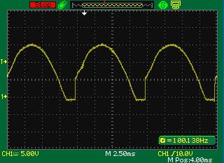
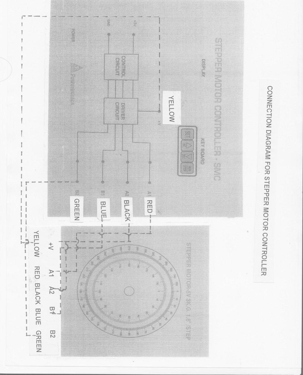
57 Experiment No: 11 Date: SPEED CONTROL OF STEPPER MOTOR AIM: To study the static characteristics of RC Half and Full wave firing circuit. APPARATUS: Stepper motor driving circuit Study unit PROCEDURE: 1) Connect A1, A2, B1 and B2 leads of stepper motor to the corresponding output terminal points. And two common terminals to +V supply. 2) Switch ON the mains supply to the unit. 3) Check the Power supplies. The unit displays WELCOME STEPPER MOTOR After few seconds it displays STOP S/R R/F H/F RPM 1 FOR FULL Stop - Corresponds to RUN/STOP selection. S/R - Corresponds to Step/RPM ( Continuous rotation) selection. R/F - Corresponds to Reverse/Forward - direction selection. H/F - Corresponds to Half step/full step selection. 4) Now RPM blinks. Press INC / DEC key to select STEP or RPM ( Continuous rotation) mode. 5) After selecting RPM/STEP mode press SET key to select the mode. Now 1 blinks. This is corresponds to number of rotation or number of steps selected. 6) Press INC/DEC key to select the speed or steps. 7) Press SET key to set the rpm / number of steps. Now FOR blinks. This is corresponds to direction of rotation Forward. Press INC/DEC key to select the direction of rotation and press SET key to select. 8) Now FULL blinks. This is corresponds to Full step. 9) Press INC/DEC key to select Half step / Full step mode and press SET key to select Half / Full step mode.now the setting is over. 10) Press RUN / STOP key, the stepper motor rotates at the set speed if RPM is selected or it moves the number of steps set and stops. 11) Again pressing RUN/ STOP key the motor stops if it is in RPM mode or it again moves the number of set steps and stops. 12) Set the step mode, 1 step, FORWARD and Half step mode. 13) Check the output status by LED indication for each step and verify with the switching logic sequence as given in the below truth table. 14) Repeat the same for Full step mode. Repeat the same for Reverse direction. 51
58 52
59 CIRCUIT DIAGRAM LOGIC CONTROLLER USING MICROCONTROLLER FREEWHEEING DIODES Red A1 WHITEE - ve Black A2 Rs + ve Blue B1 BLACK Green B2 Rs SWITCHING TRANSISTORS V = 4 X Motor Voltage Rs = 3 X Rm (Motor resistance/ Phase) Suitable for slow RPM SWITCHING LOGIC SEQUENCE Full step A1 A2 B1 B2 Red Black Blue Green Q1 Q2 Q3 Q4 Half step A1 A2 B1 B2 Red Black Blue Green To change the direction read sequence from bottom to top. 53
60 STEPPER MOTOR SPECIFICATION The stepper motor fitted on the panel and all the connections are brought to a connector. The dial is fitted to the shaft of the stepper motor. The inner dial marking in steps and outer marking in degrees. Step angle : or Kg Cm = 0.1 NM Steps per revolution : 200 Half step = VOLTAGE -5V THEORY:- The stepping motor is an electromagnetic device which converts digital pulses into discrete mechanical rotational movements. In rotary step motor, the output shaft or motor rotates in equal increments, in response to a train of input pulses. CHARACTERISTICS: Construction: Stepping Motor is basically a Motor with two phases, eight salient poles, toothed iron rotor and a permanent magnet. This rotor is known as hybrid rotor. The rotor is suspended in the stator by means of sealed ball bearings. All parts of the motors are precision machined for better performance and accuracy of steps. Step Angle: or non cumulative. Holding Torque : 2.8 Kg. Cm. Dynamic Torque: Dynamic torque is mainly controlled by the electronics control Circuits. Torque will drop down as the speed increases. Residual Torque or Detent Torque: Because of the presence of permanent magnet in the Rotor. Working Temperature and insulation Class: Temperature of stepping motors may rise 50 0 C above ambient. It is observed that body temp. Generally stabilizes at about 85 0 C to 90 0 C for continuous duty cy The insulation used is of class B type which can withstand hot spot temp. of C. For better heat dissipation motors duly fitted with heat sinks are recommended. This reduces the temp by about 10 0 C to 15 0 C. Working of Stepping Motor: The stepping action is caused by sequential switching of supply to the two phases of motor as shown in the switching logic sequence table. The specified torque of any Stepping motors is the torque at stands still (holding torque). This torque is directly proportional to the current to rated level within the time given for one step. This is mainly due to L/R time constant of winding. The drop in current level causes drop in torque as the speed increases. In order to improve torque at high speed it is necessary to maintain current at the rated level. Never exceed rated current of the motor. Stepper Motors differ form conventional DC Servo motors in the following respects: 54
61 1. There is no control winding in Stepping Motors Both windings are identical. 2. The stepping rate (Speed of rotation) is governed by frequency of switching and not by supply voltage. 3. A Single pulse input will move the shaft of Motor by one step. Thus number of steps can be precisely controlled by controlling number of pulses. 4. When there is no pulse input, the rotor will remain locked in the position in which the last step was taken since at any time two winding are always energized which lock the rotor electromagnetically. 5. Stepping Motors can be programmed in there parameters namely: a) direction, b) Speed, c) Number of Steps. 6. Stepping Motor is brushless so no wear & tear. 7. Load & no load condition makes no difference in running currents of the motor. PROCEDURE: 1) To begin with switch ON the DC Chopper firing unit. 2) Observe the test point signals and Trigger output signals by varying Duty cycle and Frequency Potentiometer. Be sure the trigger outputs are proper before connecting to the power circuit. 3) Now make the interconnections in the power circuit as given in the circuit diagram for voltage commutated chopper(impulse commutated chopper) 4) Connect DC supply from a Regulated DC power supply unit(30v/2a). 5) Connect a Resistive load (100 Ohms/2Amps Rheostat) 6) Connect respective trigger outputs from the firing circuit to the respective SCRs in the Power Circuit. 7) Initially keep the ON/OFF switch in the firing circuit in OFF position. 8) Switch ON the DC supply. Apply Main SCR trigger pulses by pressing the ON/OFF switch to ON position. 9) Observe the voltage waveforms across load. 10) We can observe the chopped DC waveform. 11) If the commutation fails we can see only the DC voltage. 12) In this case switch OFF the DC supply, Switch OFF pulses and check the connections and try again. 55
62 13) Observe the voltage across load, across Capacitor, across Main SCR and auxiliary SCR by varying Duty cycle and frequency Potentiometer. 14) Draw the wave forms at different duty cycle and at different Frequency. 15) Connect Voltmeter and Ammeter and note down values in the table. 16) Connect R-L Load and repeat the above procedure for with and without freewheeling diode. Result:- Driving circuit for Speed control of Stepper motor is constructed and its performance is studied. 56
63 Experiment No: 12 Date: IMPULSE COMMUTATED CHOPPER AIM: To study the static characteristics of RC Half and Full wave firing circuit. APPARATUS: DC chopper circuit Study unit T1 C T2 Vdc Dm LOAD. L D1 TABULAR COLUMN VOLTAGE COMMUTATED CHOPPER:- Sl. No. V in volts Ton msec T off msce Duty cycle =Ton/T in % Vo volts Io amps 57
64 Actual Waveforms for Voltage commutated chopper Vscr1 V Load V Load Vscr2 b) Waveforms 58
65 THEORY:- DC CHOPPER In many industrial applications, it is required to convert a fixed-voltage DC source into a variablevoltage DC source. A DC chopper converts directly from DC to DC and is also known as a DCto-DC converter. A chopper can be considered as DC equivalent to AC transformer with a continuously variable turns ratio. Like a transformer, it could be used to step-down or step-up a DC voltage source. Choppers are widely used for traction motor control in electric automobiles, trolley cars, marine hoists, fork-lift trucks and mine haulers. They provide smooth acceleration control, high efficiency and fast dynamic response. Chopper can be used in regenerative braking of DC motors to return energy back to the supply, and this feature results in energy savings for transportation systems with frequent stops. Choppers are also used in DC voltage regulators. Circuit Diagram VDC a) Circuit Diagram 59
66 Accessories Required :- 1) Rheostat-100 Ohms/2A. 2) DC power supply -30V/2A (Single) 3) C.R.O.-20MHZ. Procedure:- 1) To begin with switch on the power supply to the firing circuit. Check that trigger pulses by varying the frequency. 2) Make the interconnections of the power circuit as shown in the circuit diagram. 3) Now connect trigger outputs from the firing circuits to Gate and Cathode of SCR`s T1 and T2. 4) Connect input from a 30V/2A Regulated power supply. Switch on the input DC supply. Now apply trigger pulses to the SCR`s and observe voltage wave from across load. 5)Vary the frequency and observe the wave forms. 6) If the inverter frequency increases above the resonant frequency of the power circuit commutation will fail. 7)Then switch OFF the DC supply, reduce the inverter frequency and try again if you will not get the result. Check the input fuse and try again. 8) Repeat the same with different values of L, C and load. 9) And also observe the waveforms with and without fly wheel diodes. The output waveform is entirely depending on load. 10) Plot a graph of frequency verses output voltage. (Output voltage varies with frequency) 11. Tabulate the readings in the table (refer given table). 12. Draw the load voltage waveform. To switch OFF the inverter. Switch OFF the input supply first and then trigger pulses. Resonance frequency:- fr.= 1 1 _ R 2 2 π LC 4L 2 60
67 TABULAR COLUMN:- Sl No. Frequency inhz Load Voltage(AC) volts using multimeter RESULT:-DC chopper circuit have been rigged up with L and C and output waveforms across different circuit elements have been plotted. 61
68 Experiment No: 13 Date: SERIES AND PARALLEL INVERTER AIM: To study the static characteristics of RC Half and Full wave firing circuit. APPARATUS: RC Firing circuit Study unit MODIFIED SERIES INVERTER F U S E D 1 T 1 C 1 (C 2 ) S W I T C H L1 LOAD Lm 50ohms/2A L2 C 1 1 (C 1 2 ) V DC 0-30V RPS D 2 T 2 CIRCUIT DIAGRAM Low frequency eo 62


69 High frequency DIFFERENT WAVEFORMS FOR SERIES INVERTER AS OBSERVED ON DIGITAL STORAGE OSCILLOSCOPE Capacitor-10Microfarad L= 10mh R=15 Ohms app. WAVEFORM ACROSS LOAD (AT LOW FREQUENCY WITH OUT FLY WHEEL DIODES) 63

")
70 WAVEFORM ACROSS LOAD (AT HIGH FREQUENCY WITH OUT FLY WHEEL DIODES WAVEFORM ACROSS LOAD (AT LOW FREQUENCY WITH FLY WHEEL DIODES) WAVEFORM ACROSS LOAD (AT HIGH FREQUENCY WITH FLY WHEEL DIODES) 64
71 Accessories Required :- THEORY : 1) Rheostat-100 Ohms/2A. 2) DC power supply -30V/2A (Single) 3) C.R.O.-20MHZ. The circuit is a typical class C Parallel inverter. Assume T N to be ON and T p to be OFF. The bottom of the commutating capacitor is charged to twice the supply voltage and remains at this value until T P is turned on. When T P is turned on, the current flows through lower half of the primary, T P and commutating inductance L. Since voltage across C cannot instantaneously, the common SCR cathode point raises approximately to 2V dc and reverse biases T N. Thus T N turns off and C discharges through L, the supply circuit and then recharges in the reverse direction. The autotransformer action makes C to charge making now its upper point to reach +2V dc Volts ready to commutate T p, When T N is again turned on and the cycle repeats. The major purpose of commutating inductor L is to limit commutating capacitor charging current during switching. Free wheeling diodes D P and D N assist the inverter in handling a wide range of loads and the value of C may be reduced since the capacitor now does not have to carry the reactive current. To dampen the feedback diode currents within the half period, feedback diodes are connected to tapings of the transformer at 25V tapings. PROCEDURE: - 1) Switch on the firing circuit. Observe the trigger outputs TP and TN by varying frequency potentiometer and by operating ON/OFF switch. 2) Then connect input DC supply to the power circuit from DC Regulated power supply(30v/2a). 3) Connect trigger outputs to Gate and Cathode of SCR TP & TN. 4) Make the interconnections as shown in circuit diagram. 5) Connect load between load terminals(50ohms/2a). 6) Connect free wheeling diodes in the circuit. 7) To begin with set input voltage to 15V. Apply trigger pulses to SCR and observe voltage waveforms across load. 8) Output voltage is square wave only. Then remove freewheeling diode connections and observe the waveforms. 9) Then vary the load, vary the frequency and observe waveforms. To switch OFF the inverter switch OFF DC input supply only. Switch OFF the trigger pulses will lead to short circuit. 10) Since the parallel inverter works on forced commutation, there is a chance of commutation failure. 11) If the commutation fails, there is a dead short circuit in the input DC supply, which will leads to the blown off the input fuse. Please check the fuse if the 65
72 commutation fails. Preferably connect the input DC supply from the 30V/2A regulated DC power supply unit which has over current tripping facility thereby protect the DC supply unit. 12) If the commutation fails, switch off the DC supply first and then trigger Outputs. Check the connections again. CIRCUIT DIAGRAM: D1 30V SCR1 25V 0 _ VDC + L SCR2 C 0V 25V 30V RL 30V D2 TRIGGER OUTPUTS T 1 T 2 +V DC --V DC 66
73 DIFFERENT WAVEFORMS FOR PARALLEL INVERTER AS OBSERVED ON DIGITAL STORAGE OSCILLOSCOPE LOAD VOLTAGE WAVEFORM FOR WITHOUT FREEWHEELING DIODE 67


74 VOLTAGE WAVEFORM AT PRIMARY OF TRANSFORMER WITHOUT FREEWHEELING DIODE LOAD VOLTAGE WAVEFORM FOR WITH FREEWHEELING DIODE VOLTAGE WAVEFORM AT PRIMARY OF TRANSFORMER 68

75 WITH FREEWHEELING DIODE VOLTAGE WAVEFORM ACROSS SCR s TP&TN WITH FREEWHEELING DIODE RESULT:-Series and Parallel Inverter circuits have been rigged up with L and C and output waveforms across different circuit elements have been plotted. 69
S.J.P.N Trust's. Hirasugar Institute of Technology, Nidasoshi
 S.J.P.N Trust's Hirasugar Institute of Technology, Nidasoshi Inculcating Values, Promoting Prosperity Approved by AICTE New Delhi, Recognized by Govt. of Karnataka and Affiliated to VTU Belagavi Tq: Hukkeri
POWER ELECTRONICS LAB
 MUFFAKHAM JAH COLLEGE OF ENGINEERING & TECHNOLOGY Banjara Hills Road No 3, Hyderabad 34 www.mjcollege.ac.in DEPARTMENT OF ELECTRICAL ENGINEERING LABORATORY MANUAL POWER ELECTRONICS LAB For B.E. III/IV
LENDI INSTITUTE OF ENGINEERING & TECHNOLOGY
 LENDI INSTITUTE OF ENGINEERING & TECHNOLOGY (Approved by A.I.C.T.E & Affiliated to JNTU,Kakinada) Jonnada (Village), Denkada (Mandal), Vizianagaram Dist 535 005 Phone No. 08922-241111, 241112 E-Mail: lendi_2008@yahoo.com
POWER ELECTRONICS LAB MANUAL
 JIS College of Engineering (An Autonomous Institution) Department of Electrical Engineering POWER ELECTRONICS LAB MANUAL Exp-1. Study of characteristics of an SCR AIM: To obtain the V-I characteristics
CHADALAWADA RAMANAMMA ENGINEERING COLLEGE (AUTONOMOUS) Chadalawada Nagar, Renigunta Road, Tirupati
 Chadalawada Nagar, Renigunta Road, Tirupati") ELECTRONIC DEVICES AND CIRCUITS LABORATORY MANUAL Subject Code : 17CA04305 Regulations : R17 Class : III Semester (ECE) CHADALAWADA RAMANAMMA ENGINEERING COLLEGE (AUTONOMOUS) Chadalawada Nagar, Renigunta
ELECTRONIC DEVICES AND CIRCUITS LABORATORY MANUAL Subject Code : 17CA04305 Regulations : R17 Class : III Semester (ECE) CHADALAWADA RAMANAMMA ENGINEERING COLLEGE (AUTONOMOUS) Chadalawada Nagar, Renigunta
6. Explain control characteristics of GTO, MCT, SITH with the help of waveforms and circuit diagrams.
 POWER ELECTRONICS QUESTION BANK Unit 1: Introduction 1. Explain the control characteristics of SCR and GTO with circuit diagrams, and waveforms of control signal and output voltage. 2. Explain the different
SSM INSTITUTE OF ENGINEERING AND TECHNOLOGY DINDIGUL PALANI HIGH WAY, SINTHALAGUNDU POST DINDIGUL
 SSM INSTITUTE OF ENGINEERING AND TECHNOLOGY DINDIGUL PALANI HIGH WAY, SINTHALAGUNDU POST DINDIGUL 624002 DEPARTMENT OF ELECTRICAL AND ELECTRONICS ENGINEERING LABORATORY MANUAL CLASS : III rd YEAR EEE SEMESTER
List of Experiments. 1. Steady state characteristics of SCR, IGBT and MOSFET. (Single phase half wave rectifier). (Simulation and hardware).
. (Simulation and hardware).") (Scheme-2013) List of Experiments 1. Steady state characteristics of SCR, IGBT and MOSFET 2. nalog and digital firing methods for SCR (Single phase half wave rectifier). (Simulation and hardware). 3. Full
(Scheme-2013) List of Experiments 1. Steady state characteristics of SCR, IGBT and MOSFET 2. nalog and digital firing methods for SCR (Single phase half wave rectifier). (Simulation and hardware). 3. Full
Dev Bhoomi Institute Of Technology Department of Electronics and Communication Engineering PRACTICAL INSTRUCTION SHEET
 Dev Bhoomi Institute Of Technology Department of Electronics and Communication Engineering PRACTICAL INSTRUCTION SHEET LABORATORY MANUAL EXPERIMENT NO. ISSUE NO. : ISSUE DATE: REV. NO. : REV. DATE : PAGE:
Basic Electronics Prof. T.S. Natarajan Department of Physics Indian Institute of Technology, Madras
 Basic Electronics Prof. T.S. Natarajan Department of Physics Indian Institute of Technology, Madras Lecture 39 Silicon Controlled Rectifier (SCR) (Construction, characteristics (Dc & Ac), Applications,
Shankersinh Vaghela Bapu Institute of Technology INDEX
 Shankersinh Vaghela Bapu Institute of Technology Diploma EE Semester III 3330905: ELECTRONIC COMPONENTS AND CIRCUITS INDEX Sr. No. Title Page Date Sign Grade 1 Obtain I-V characteristic of Diode. 2 To
10ECL78-Power Electronics Lab
 Circuit Diagram-1: Circuit Diagram-2: To find the Latching Current: Dept. of ECE, CIT, Gubbi Page No. 1 Experiment No. 1 a) Static Characteristics of SCR Static Characteristics of SCR and DIAC Date: /
POWER ELECTRONICSAND SIMULATION LAB 3 rd YEAR-II SEMESTER
 POWER ELECTRONICSAND SIMULATION LAB 3 rd YEAR-II SEMESTER NAME OF THE STUDENT : REGISTERNUMBER : YEAR/ SEMESTER : STAFF INCHARGE : Mr. G.SRIDHAR BABU Assoc.Prof/EEE 1 General Instructions to students for
Power Electronics (BEG335EC )
") 1 Power Electronics (BEG335EC ) 2 PURWANCHAL UNIVERSITY V SEMESTER FINAL EXAMINATION - 2003 The figures in margin indicate full marks. Attempt any FIVE questions. Q. [1] [a] A single phase full converter
1 Power Electronics (BEG335EC ) 2 PURWANCHAL UNIVERSITY V SEMESTER FINAL EXAMINATION - 2003 The figures in margin indicate full marks. Attempt any FIVE questions. Q. [1] [a] A single phase full converter
TPCT S College of Engineering, Osmanabad. Laboratory Manual. Power Electronics. For. Third Year Students. Manual Prepared by Prof. S. G.
 TPCT S College of Engineering, Osmanabad Laboratory Manual Power Electronics For Third Year Students Manual Prepared by Prof. S. G. Shinde Author COE, Osmanabad TPCT s College of Engineering Solapur Road,
SCR Triggering Techniques Scientech 2703
 SCR Triggering Techniques Scientech 2703 Learning Material Ver 1.1 An ISO 9001:2008 company Scientech Technologies Pvt. Ltd. 94, Electronic Complex, Pardesipura, Indore - 452 010 India, + 91-731 4211100,
Operating Manual Ver.1.1
 SCR Triggering Techniques ST2703 Operating Manual Ver.1.1 An ISO 9001 : 2000 company 94-101, Electronic Complex Pardesipura, Indore- 452010, India Tel : 91-731- 2570301/02, 4211100 Fax: 91-731- 2555643
Power Electronics (Sample Questions) Module-1
 Module-1") Module-1 Short Questions (Previous Years BPUT Questions 1 to 18) 1. What are the conditions for a thyristor to conduct? di 2. What is the common method used for protection? dt 3. What is the importance
Module-1 Short Questions (Previous Years BPUT Questions 1 to 18) 1. What are the conditions for a thyristor to conduct? di 2. What is the common method used for protection? dt 3. What is the importance
UNIVERSITY QUESTIONS. Unit-1 Introduction to Power Electronics
 UNIVERSITY QUESTIONS Unit-1 Introduction to Power Electronics 1. Give the symbol and characteristic features of the following devices. (i) SCR (ii) GTO (iii) TRIAC (iv) IGBT (v) SIT (June 2012) 2. What
Power Electronics Power semiconductor devices. Dr. Firas Obeidat
 Power Electronics Power semiconductor devices Dr. Firas Obeidat 1 Table of contents 1 Introduction 2 Classifications of Power Switches 3 Power Diodes 4 Thyristors (SCRs) 5 The Triac 6 The Gate Turn-Off
 http://www.electronics-tutorials.ws/power/triac.html Triac Tutorial and Basic Principles In the previous tutorial we looked at the construction and operation of the Silicon Controlled Rectifier more commonly
Power Semiconductor Devices
 TRADEMARK OF INNOVATION Power Semiconductor Devices Introduction This technical article is dedicated to the review of the following power electronics devices which act as solid-state switches in the circuits.
Experiment DC-DC converter
 POWER ELECTRONIC LAB Experiment-7-8-9 DC-DC converter Power Electronics Lab Ali Shafique, Ijhar Khan, Dr. Syed Abdul Rahman Kashif 10/11/2015 This manual needs to be completed before the mid-term examination.
Dr.Arkan A.Hussein Power Electronics Fourth Class. Commutation of Thyristor-Based Circuits Part-I
 Commutation of Thyristor-Based Circuits Part-I ١ This lesson provides the reader the following: (i) (ii) (iii) (iv) Requirements to be satisfied for the successful turn-off of a SCR The turn-off groups
INSTITUTE OF AERONAUTICAL ENGINEERING (Autonomous) Dundigal, Hyderabad
 Dundigal, Hyderabad") I INSTITUTE OF AERONAUTICAL ENGINEERING (Autonomous) Dundigal, Hyderabad-000 DEPARTMENT OF ELECTRICAL AND ELECTRONICS ENGINEERING TUTORIAL QUESTION BANK Course Name : POWER ELECTRONICS Course Code : AEE0
I INSTITUTE OF AERONAUTICAL ENGINEERING (Autonomous) Dundigal, Hyderabad-000 DEPARTMENT OF ELECTRICAL AND ELECTRONICS ENGINEERING TUTORIAL QUESTION BANK Course Name : POWER ELECTRONICS Course Code : AEE0
Experiment (1) Principles of Switching
 Principles of Switching") Experiment (1) Principles of Switching Introduction When you use microcontrollers, sometimes you need to control devices that requires more electrical current than a microcontroller can supply; for this,
Experiment (1) Principles of Switching Introduction When you use microcontrollers, sometimes you need to control devices that requires more electrical current than a microcontroller can supply; for this,
SCR- SILICON CONTROLLED RECTIFIER
 SCR- SILICON CONTROLLED RECTIFIER Definition: When a pn junction is added to a junction transistor, the resulting three pn junction device is called a silicon controlled rectifier. SCR can change alternating
UNIT II JFET, MOSFET, SCR & UJT
 UNIT II JFET, MOSFET, SCR & UJT JFET JFET as an Amplifier and its Output Characteristics JFET Applications MOSFET Working Principles, SCR Equivalent Circuit and V-I Characteristics. SCR as a Half wave
UNIT 3: FIELD EFFECT TRANSISTORS
 FIELD EFFECT TRANSISTOR: UNIT 3: FIELD EFFECT TRANSISTORS The field effect transistor is a semiconductor device, which depends for its operation on the control of current by an electric field. There are
EE6611- POWER ELECTRONICS AND DRIVES
 Dharmapuri 636 703 LAB MANUAL Regulation : 203 Branch : B.E - EEE Year & Semester : III Year / VI Semester EE66- POWER ELECTRONICS AND DRIVES LABORATORY 2 ANNA UNIVERSITY SYLLABUS (203 REGULATION) SEMESTER
Learn about the use, operation and limitations of thyristors, particularly triacs, in power control
 Exotic Triacs: The Gate to Power Control Learn about the use, operation and limitations of thyristors, particularly triacs, in power control D. Mohan Kumar Modern power control systems use electronic devices
Government Polytechnic Muzaffarpur Name of the Lab: Applied Electronics Lab
 Government Polytechnic Muzaffarpur Name of the Lab: Applied Electronics Lab Subject Code: 1620408 Experiment-1 Aim: To obtain the characteristics of field effect transistor (FET). Theory: The Field Effect
2 Marks - Question Bank. Unit 1- INTRODUCTION
 Two marks 1. What is power electronics? EE6503 POWER ELECTRONICS 2 Marks - Question Bank Unit 1- INTRODUCTION Power electronics is a subject that concerns the applications electronics principles into situations
ELECTRONIC DEVICES AND CIRCUITS LABORATORY MANUAL FOR II / IV B.E (EEE): I - SEMESTER
: I - SEMESTER") ELECTRONIC DEVICES AND CIRCUITS LABORATORY MANUAL FOR II / IV B.E (EEE): I - SEMESTER DEPT. OF ELECTRICAL AND ELECTRONICS ENGINEERING SIR C.R.REDDY COLLEGE OF ENGINEERING ELURU 534 007 ELECTRONIC DEVICES
ELECTRONIC DEVICES AND CIRCUITS LABORATORY MANUAL FOR II / IV B.E (EEE): I - SEMESTER DEPT. OF ELECTRICAL AND ELECTRONICS ENGINEERING SIR C.R.REDDY COLLEGE OF ENGINEERING ELURU 534 007 ELECTRONIC DEVICES
Objective: To study and verify the functionality of a) PN junction diode in forward bias. Sl.No. Name Quantity Name Quantity 1 Diode
 PN junction diode in forward bias. Sl.No. Name Quantity Name Quantity 1 Diode") Experiment No: 1 Diode Characteristics Objective: To study and verify the functionality of a) PN junction diode in forward bias Components/ Equipments Required: b) Point-Contact diode in reverse bias Components
Experiment No: 1 Diode Characteristics Objective: To study and verify the functionality of a) PN junction diode in forward bias Components/ Equipments Required: b) Point-Contact diode in reverse bias Components
 ANNA UNIVERSITY, Chennai 2013 REGULATION DEPARTMENT OF ELECTRONICS & COMMUNICATION ENGG. EC6211 CIRCUITS AND DEVICES LABORATORY (I B.E II Semester Batch 2013) EC6211 CIRCUITS AND DEVICES LABORATORY List
ELECTRIC DRIVE LAB Laboratory Manual
 DEV BHOOMI INSTITUTE OF TECHNOLOGY CHAKRATA ROAD, NAVGAOUN MANDUWALA, UTTARAKHAND Programs: B.TECH. (Electrical and Electronics Engineering) ELECTRIC DRIVE LAB Laboratory Manual PREPARED BY ASHISH KUKRETI,
Logic Gates & Training Boards
 Logic Gates & Training Boards ANALOG TO DIGITAL (A/D) CONVERTOR (ELP.112.140) Objective : To study Analog to Digital & Digital to Analog convertors using R-2R network & Successive Approximation Method.
OBJECTIVE TYPE QUESTIONS
 OBJECTIVE TYPE QUESTIONS Q.1 The breakdown mechanism in a lightly doped p-n junction under reverse biased condition is called (A) avalanche breakdown. (B) zener breakdown. (C) breakdown by tunnelling.
FAMILIARISATION WITH P.E. COMPONENTS
 FAMILIARISATION WITH P.E. COMPONENTS A. SINGLE PHASE PAC USING TRIAC. Object : To study a) The triggering circuit of an A.C. phase angle controller using a triac. b) The performance with a resistive load.
Emitter base bias. Collector base bias Active Forward Reverse Saturation forward Forward Cut off Reverse Reverse Inverse Reverse Forward
 SEMICONDUCTOR PHYSICS-2 [Transistor, constructional characteristics, biasing of transistors, transistor configuration, transistor as an amplifier, transistor as a switch, transistor as an oscillator] Transistor
FREQUENTLY ASKED QUESTIONS
 FREQUENTLY ASKED QUESTIONS UNIT-1 SUBJECT : ELECTRONIC DEVICES AND CIRCUITS SUBJECT CODE : EC6202 BRANCH: EEE PART -A 1. What is meant by diffusion current in a semi conductor? (APR/MAY 2010, 2011, NOV/DEC
GOVERNMENT OF KARNATAKA KARNATAKA STATE PRE-UNIVERSITY EDUCATION EXAMINATION BOARD II YEAR PUC EXAMINATION MARCH-2013 SCHEME OF VALUATION
 GOVERNMENT OF KARNATAKA KARNATAKA STATE PRE-UNIVERSITY EDUCATION EXAMINATION BOARD II YEAR PUC EXAMINATION MARCH-03 SCHEME OF VALUATION Subject Code: 0 Subject: PART - A 0. What does the arrow mark indicate
UNIT I POWER SEMI-CONDUCTOR DEVICES
 UNIT I POWER SEMI-CONDUCTOR DEVICES SUBJECT CODE SUBJECT NAME STAFF NAME : EE6503 : Power Electronics : Ms.M.Uma Maheswari 1 SEMICONDUCTOR DEVICES POWER DIODE POWER TRANSISTORS POWER BJT POWER MOSFET IGBT
Electronic & Telecommunication Engineering
 Department of Electronic & Telecommunication Engineering LAB MANUAL ADC B.Tech 3rd Semester KCT College of Engineering & Technology Village Fatehgarh (Distt. Sangrur) INDEX List Of Experiment To construct
DLVP A OPERATOR S MANUAL
 DLVP-50-300-3000A OPERATOR S MANUAL DYNALOAD DIVISION 36 NEWBURGH RD. HACKETTSTOWN, NJ 07840 PHONE (908) 850-5088 FAX (908) 908-0679 TABLE OF CONTENTS INTRODUCTION...3 SPECIFICATIONS...5 MODE SELECTOR
(a) average output voltage (b) average output current (c) average and rms values of SCR current and (d) input power factor. [16]
![(a) average output voltage (b) average output current (c) average and rms values of SCR current and (d) input power factor. [16]](/thumbs/81/83006678.jpg "(a) average output voltage (b) average output current (c) average and rms values of SCR current and (d) input power factor. [16]") Code No: 07A50204 R07 Set No. 2 1. A single phase fully controlled bridge converter is operated from 230 v, 50 Hz source. The load consists of 10Ω and a large inductance so as to reach the load current
Code No: 07A50204 R07 Set No. 2 1. A single phase fully controlled bridge converter is operated from 230 v, 50 Hz source. The load consists of 10Ω and a large inductance so as to reach the load current
Shankersinh Vaghela Bapu Institute of Technology
 Shankersinh Vaghela Bapu Institute of Technology B.E. Semester III (EC) 131101: Basic Electronics INDEX Sr. No. Title Page Date Sign Grade 1 [A] To Study the V-I characteristic of PN junction diode. [B]
REV NO EXPERIMENT NO 1 AIM: To study the PN junction diode characteristics under Forward & Reverse bias conditions. APPARATUS REQUIRED:
 KARNAL INSTITUTE OF TECHNOLOGY & MANAGEMENT KUNJPURA, KARNAL LAB MANUAL OF ------- SUBJECT CODE DATE OF ISSUE: SEMESTER: BRANCH: REV NO EXPERIMENT NO 1 AIM: To study the PN junction diode characteristics
EXPERIMENT 5 : DIODES AND RECTIFICATION
 EXPERIMENT 5 : DIODES AND RECTIFICATION Component List Resistors, one of each o 2 1010W o 1 1k o 1 10k 4 1N4004 (Imax = 1A, PIV = 400V) Diodes Center tap transformer (35.6Vpp, 12.6 VRMS) 100 F Electrolytic
Analog and Telecommunication Electronics
 Politecnico di Torino - ICT School Analog and Telecommunication Electronics F2 Active power devices»mos»bjt» IGBT, TRIAC» Safe Operating Area» Thermal analysis 30/05/2012-1 ATLCE - F2-2011 DDC Lesson F2:
EXPERIMENT 7: DIODE CHARACTERISTICS AND CIRCUITS 10/24/10
 DIODE CHARACTERISTICS AND CIRCUITS EXPERIMENT 7: DIODE CHARACTERISTICS AND CIRCUITS 10/24/10 In this experiment we will measure the I vs V characteristics of Si, Ge, and Zener p-n junction diodes, and
HIGH LOW Astable multivibrators HIGH LOW 1:1
 1. Multivibrators A multivibrator circuit oscillates between a HIGH state and a LOW state producing a continuous output. Astable multivibrators generally have an even 50% duty cycle, that is that 50% of
Prof. Steven S. Saliterman Introductory Medical Device Prototyping
 Introductory Medical Device Prototyping Department of Biomedical Engineering, University of Minnesota http://saliterman.umn.edu/ Solid state power switching: Silicon controlled rectifiers (SCR or Thyristor).
Electrical And Electronics Engg
 Electrical And Electronics Engg Rectifier Cubical panel type Voltage 3Ph 440V /(0-300V) DC 3Ph Isolation transformer-20kva Thyristor rating Current -300A/PIV - 1500V over load protection and necessary
Pre-certification Electronics Questions. Answer the following with the MOST CORRECT answer.
 Electronics Questions Answer the following with the MOST CORRECT answer. 1. The cathode end terminal of a semiconductor diode can be identified by: a. the negative sign marked on the case b. a circular
IFB270 Advanced Electronic Circuits
 IFB270 Advanced Electronic Circuits Chapter 11: Thyristors Prof. Manar Mohaisen Department of EEC Engineering Review of the Precedent Lecture To introduce several concepts on capacitance in amplifiers
POWER ELECTRONICS. Alpha. Science International Ltd. S.C. Tripathy. Oxford, U.K.
 POWER ELECTRONICS S.C. Tripathy Alpha Science International Ltd. Oxford, U.K. Contents Preface vii 1. SEMICONDUCTOR DIODE THEORY 1.1 1.1 Introduction 1.1 1.2 Charge Densities in a Doped Semiconductor 1.1
Practical Manual. Deptt.of Electronics &Communication Engg. (ECE)
") Practical Manual LAB: BASICS OF ELECTRONICS 1 ST SEM.(CSE/CV) Deptt.of Electronics &Communication Engg. (ECE) RAO PAHALD SINGH GROUP OF INSTITUTIONS BALANA(MOHINDER GARH)12302 Prepared By. Mr.SANDEEP KUMAR
Practical Manual LAB: BASICS OF ELECTRONICS 1 ST SEM.(CSE/CV) Deptt.of Electronics &Communication Engg. (ECE) RAO PAHALD SINGH GROUP OF INSTITUTIONS BALANA(MOHINDER GARH)12302 Prepared By. Mr.SANDEEP KUMAR
Federal Urdu University of Arts, Science & Technology Islamabad Pakistan SECOND SEMESTER ELECTRONICS - I
 SECOND SEMESTER ELECTRONICS - I BASIC ELECTRICAL & ELECTRONICS LAB DEPARTMENT OF ELECTRICAL ENGINEERING Prepared By: Checked By: Approved By: Engr. Yousaf Hameed Engr. M.Nasim Khan Dr.Noman Jafri Lecturer
SINGLE PHASE CURRENT SOURCE INVERTER (C.S.I)
") Power Electronics Laboratory SINGLE PHASE CURRENT SOURCE INVERTER (C.S.I) OBJECT: To study the gate firing pulses. To observe and measure the voltages across the Thyristors and across the Load for a current
Power Electronics Laboratory SINGLE PHASE CURRENT SOURCE INVERTER (C.S.I) OBJECT: To study the gate firing pulses. To observe and measure the voltages across the Thyristors and across the Load for a current
THIRD SEMESTER ELECTRONICS - II BASIC ELECTRICAL & ELECTRONICS LAB DEPARTMENT OF ELECTRICAL ENGINEERING
 THIRD SEMESTER ELECTRONICS - II BASIC ELECTRICAL & ELECTRONICS LAB DEPARTMENT OF ELECTRICAL ENGINEERING Prepared By: Checked By: Approved By: Engr. Saqib Riaz Engr. M.Nasim Khan Dr.Noman Jafri Lecturer
1. LINEAR WAVE SHAPING
 Aim: 1. LINEAR WAVE SHAPING i) To design a low pass RC circuit for the given cutoff frequency and obtain its frequency response. ii) To observe the response of the designed low pass RC circuit for the
Experiment No. 2 Half Wave Rectifier using RC-Triggering
 Experiment No. 2 Half Wave Rectifier using RC-Triggering Pre-Lab Reading: 1. Power Electronics: Circuits, Devices and Applications, by M. H. Rashid, 3e. (See page 790 to get help for this experiment).
Field - Effect Transistor
 Page 1 of 6 Field - Effect Transistor Aim :- To draw and study the out put and transfer characteristics of the given FET and to determine its parameters. Apparatus :- FET, two variable power supplies,
ANALOG ELECTRONIC CIRCUITS LABORATORY MANUAL (CODE: EEE - 228)
") ANALOG ELECTRONIC CIRCUITS LABORATORY MANUAL (CODE: EEE - 228) DEPARTMENT OF ELECTRONICS & COMMUNICATION ENGINEERING ANIL NEERUKONDA INSTITUTE OF TECHNOLOGY & SCIENCES (Affiliated to AU, Approved by AICTE
ANALOG ELECTRONIC CIRCUITS LABORATORY MANUAL (CODE: EEE - 228) DEPARTMENT OF ELECTRONICS & COMMUNICATION ENGINEERING ANIL NEERUKONDA INSTITUTE OF TECHNOLOGY & SCIENCES (Affiliated to AU, Approved by AICTE
AN1003. Phase Control Using Thyristors. Introduction. Output Power Characteristics
 AN13 AN139 Phase Control Using Thyristors Introduction Due to high-volume production techniques, thyristors are now priced so that almost any electrical product can benefit from electronic control. A look
Study of 1-phase AC to DC controlled converter (both fully controlled And half controlled)
") Study of 1-phase AC to DC controlled converter (both fully controlled And half controlled) Object: To study the performances of single phase half-controlled bridge Rectifier. A. In configuration A. B.
Study of 1-phase AC to DC controlled converter (both fully controlled And half controlled) Object: To study the performances of single phase half-controlled bridge Rectifier. A. In configuration A. B.
COLLECTOR DRAIN BASE GATE EMITTER. Applying a voltage to the Gate connection allows current to flow between the Drain and Source connections.
 MOSFETS Although the base current in a transistor is usually small (< 0.1 ma), some input devices (e.g. a crystal microphone) may be limited in their output. In order to overcome this, a Field Effect Transistor
DHANALAKSHMI COLLEGE OF ENGINEERING DEPARTMENT OF ELECTRICAL AND ELECTRONICS ENGINEERING EC6202 ELECTRONIC DEVICES AND CIRCUITS
 DHANALAKSHMI COLLEGE OF ENGINEERING DEPARTMENT OF ELECTRICAL AND ELECTRONICS ENGINEERING EC6202 ELECTRONIC DEVICES AND CIRCUITS UNIT-I - PN DIODEAND ITSAPPLICATIONS 1. What is depletion region in PN junction?
ELECTRONICS DEVICE MANUAL (NEC-354)
") ELECTRONICS DEVICE MANUAL (NEC-354) DEPARTMENT OF ELECTRONICS & COMMUNICATION ENGINEERING 27, Knowledge Park-III, Greater Noida, (U.P.) Phone : 0120-2323854-58 website :- www.dronacharya.info CONTENTS
ELECTRONICS DEVICE MANUAL (NEC-354) DEPARTMENT OF ELECTRONICS & COMMUNICATION ENGINEERING 27, Knowledge Park-III, Greater Noida, (U.P.) Phone : 0120-2323854-58 website :- www.dronacharya.info CONTENTS
EXPERIMENT 5 : THE DIODE
 EXPERIMENT 5 : THE DIODE Component List Resistors, one of each o 1 10 10W o 1 1k o 1 10k 4 1N4004 (I max = 1A, PIV = 400V) Diodes Center tap transformer (35.6V pp, 12.6 V RMS ) 100 F Electrolytic Capacitor
Circuit operation Let s look at the operation of this single diode rectifier when connected across an alternating voltage source v s.
 Diode Rectifier Circuits One of the important applications of a semiconductor diode is in rectification of AC signals to DC. Diodes are very commonly used for obtaining DC voltage supplies from the readily
Lesson 1 of Chapter Three Single Phase Half and Fully Controlled Rectifier
 Lesson of Chapter hree Single Phase Half and Fully Controlled Rectifier. Single phase fully controlled half wave rectifier. Resistive load Fig. :Single phase fully controlled half wave rectifier supplying
Difference between BJTs and FETs. Junction Field Effect Transistors (JFET)
") Difference between BJTs and FETs Transistors can be categorized according to their structure, and two of the more commonly known transistor structures, are the BJT and FET. The comparison between BJTs
Difference between BJTs and FETs Transistors can be categorized according to their structure, and two of the more commonly known transistor structures, are the BJT and FET. The comparison between BJTs
Presentation Content Review of Active Clamp and Reset Technique in Single-Ended Forward Converters Design Material/Tools Design procedure and concern
 Active Clamp Forward Converters Design Using UCC2897 Hong Huang August 2007 1 Presentation Content Review of Active Clamp and Reset Technique in Single-Ended Forward Converters Design Material/Tools Design
Application Note AN-3006 Optically Isolated Phase Controlling Circuit Solution
 www.fairchildsemi.com Application Note AN-3006 Optically Isolated Phase Controlling Circuit Solution Introduction Optocouplers simplify logic isolation from the ac line, power supply transformations, and
Unijunction Transistor. T.Y.B.Sc - Eletronics POWER ELETRONICS
 Unijunction Transistor T.Y.B.Sc - Eletronics POWER ELETRONICS Unijunction Transistor Symbol and Construction The Unijunction Transistor is solid state three terminal device that can be used in gate pulse,
Basic Electronics Learning by doing Prof. T.S. Natarajan Department of Physics Indian Institute of Technology, Madras
 Basic Electronics Learning by doing Prof. T.S. Natarajan Department of Physics Indian Institute of Technology, Madras Lecture 38 Unit junction Transistor (UJT) (Characteristics, UJT Relaxation oscillator,
BREAKDOWN DEVICES. Learning Objectives
 C H A P T E R64 Learning Objectives What are Breakdown Devices? Unijunction Transistor UJT Relaxation Oscillator Programmable UJT(PUT) Silicon Controlled Rectifier Comparison between Transistors and Thyristors
Experiment No. 1 Half Wave Rectifier using R-Triggering
 Experiment No. 1 Half Wave Rectifier using R-Triggering Pre-Lab Reading: Power Electronics: Circuits, Devices and Applications, by M. H. Rashid, 3e. Objectives: To analyze resistive firing/triggering of
Contents. Acknowledgments. About the Author
 Contents Figures Tables Preface xi vii xiii Acknowledgments About the Author xv xvii Chapter 1. Basic Mathematics 1 Addition 1 Subtraction 2 Multiplication 2 Division 3 Exponents 3 Equations 5 Subscripts
EXPERIMENT 5 : THE DIODE
 EXPERIMENT 5 : THE DIODE Component List Resistors, one of each o 1 10 10W o 1 1k o 1 10k 4 1N4004 (Imax = 1A, PIV = 400V) Diodes Center tap transformer (35.6Vpp, 12.6 VRMS) 100 F Electrolytic Capacitor
Electronic devices & circuits
 Dundigal, Quthbullapur (M), Hyderabad 43 LABORATORY MANUAL Electronic devices & circuits II B.TECH -I Semester (ECE) AY-2017-2018 DEPARTMENT OF ECE MARRI LAXMAN REDDY INSTITUTE OF TECHNOLOGY & MANAGEMENT
Electrical, Electronic and Communications Engineering Technology/Technician CIP Task Grid
 Secondary Task List 100 SAFETY 101 Describe OSHA safety regulations. 102 Identify, select, and demonstrate proper hand tool use for electronics work. 103 Recognize the types and usages of fire extinguishers.
University Visvesvaraya College of Engineering
 University Visvesvaraya College of Engineering K.R.Circle, -560001 INVITATION FOR QUOTATION TEQIP-II/2013/KA2G01/Shopping/25 29-Nov-2013 To, Sub: Invitation for Quotations for supply of Goods Dear Sir,
Analog Electronic Circuits Lab-manual
 2014 Analog Electronic Circuits Lab-manual Prof. Dr Tahir Izhar University of Engineering & Technology LAHORE 1/09/2014 Contents Experiment-1:...4 Learning to use the multimeter for checking and indentifying
15EE301J- POWER ELECTRONICS LAB
 15EE301J- POWER ELECTRONICS LAB RECORD NOTEBOOK SEMESTER V DEPARTMENT OF ELECTRICAL AND ELECTRONICS ENGINEERING SRM UNIVERSITY KATTANKULATHUR-603203 POWER ELECTRONICS LABORATORY L T P C 15EE301J Total
the reactance of the capacitor, 1/2πfC, is equal to the resistance at a frequency of 4 to 5 khz.
 EXPERIMENT 12 INTRODUCTION TO PSPICE AND AC VOLTAGE DIVIDERS OBJECTIVE To gain familiarity with PSPICE, and to review in greater detail the ac voltage dividers studied in Experiment 14. PROCEDURE 1) Connect
Solid State Devices- Part- II. Module- IV
 Solid State Devices- Part- II Module- IV MOS Capacitor Two terminal MOS device MOS = Metal- Oxide- Semiconductor MOS capacitor - the heart of the MOSFET The MOS capacitor is used to induce charge at the
CRO AIM:- To study the use of Cathode Ray Oscilloscope (CRO).
.") 1. 1 To study CRO. CRO AIM:- To study the use of Cathode Ray Oscilloscope (CRO). Apparatus: - C.R.O, Connecting probe (BNC cable). Theory:An CRO is easily the most useful instrument available for testing
1. 1 To study CRO. CRO AIM:- To study the use of Cathode Ray Oscilloscope (CRO). Apparatus: - C.R.O, Connecting probe (BNC cable). Theory:An CRO is easily the most useful instrument available for testing
EEL 5245 POWER ELECTRONICS I Lecture #4: Chapter 2 Switching Concepts and Semiconductor Overview
 EEL 5245 POWER ELECTRONICS I Lecture #4: Chapter 2 Switching Concepts and Semiconductor Overview Objectives of Lecture Switch realizations Objective is to focus on terminal characteristics Blocking capability
Dev Bhoomi Institute Of Technology Department of Electronics and Communication Engineering PRACTICAL INSTRUCTION SHEET REV. NO. : REV.
 Dev Bhoomi Institute Of Technology Department of Electronics and Communication Engineering PRACTICAL INSTRUCTION SHEET LABORATORY MANUAL EXPERIMENT NO. ISSUE NO. : ISSUE DATE: July 200 REV. NO. : REV.
DOWNLOAD PDF POWER ELECTRONICS DEVICES DRIVERS AND APPLICATIONS
 Chapter 1 : Power Electronics Devices, Drivers, Applications, and Passive theinnatdunvilla.com - Google D Download Power Electronics: Devices, Drivers and Applications By B.W. Williams - Provides a wide
AE103 ELECTRONIC DEVICES & CIRCUITS DEC 2014
 Q.2 a. State and explain the Reciprocity Theorem and Thevenins Theorem. a. Reciprocity Theorem: If we consider two loops A and B of network N and if an ideal voltage source E in loop A produces current
Questions on JFET: 1) Which of the following component is a unipolar device?
 Which of the following component is a unipolar device?") Questions on JFET: 1) Which of the following component is a unipolar device? a) BJT b) FET c) DJT d) EFT 2) Current Conduction in FET takes place due e) Majority charge carriers only f) Minority charge
Questions on JFET: 1) Which of the following component is a unipolar device? a) BJT b) FET c) DJT d) EFT 2) Current Conduction in FET takes place due e) Majority charge carriers only f) Minority charge
4. Forward bias of a silicon P-N junction will produce a barrier voltage of approximately how many volts? A. 0.2 B. 0.3 C. 0.7 D. 0.
 1. The dc current through each diode in a bridge rectifier equals A. the load current B. half the dc load current C. twice the dc load current D. one-fourth the dc load current 2. When matching polarity
Other Electronic Devices
 Other Electronic Devices 1 Contents Field-Effect Transistors(FETs) - JFETs - MOSFETs Insulate Gate Bipolar Transistors(IGBTs) H-bridge driver and PWM Silicon-Controlled Rectifiers(SCRs) TRIACs Device Selection
THIRD SEMESTER DIPLOMA EXAMINATION IN ELECTRICAL & ELECTRONICS ENGINEERING, MARCH 2013 ELECTRONIC DEVICES AND CIRCUITS
 REVISION-2010 Reg. No SUB CODE:3053 Signature THIRD SEMESTER DIPLOMA EXAMINATION IN ELECTRICAL & ELECTRONICS ENGINEERING, MARCH 2013 ELECTRONIC DEVICES AND CIRCUITS Time :3hours Maximum marks:100 PART
UNIVERSITY OF TECHNOLOGY, JAMAICA School of Engineering -
 UNIVERSITY OF TECHNOLOGY, JAMAICA School of Engineering - Electrical Engineering Science Laboratory Manual Table of Contents Safety Rules and Operating Procedures... 3 Troubleshooting Hints... 4 Experiment