THIRD SEMESTER ELECTRONICS - II BASIC ELECTRICAL & ELECTRONICS LAB DEPARTMENT OF ELECTRICAL ENGINEERING
|
|
|
- Garey Strickland
- 6 years ago
- Views:
Transcription

1 THIRD SEMESTER ELECTRONICS - II BASIC ELECTRICAL & ELECTRONICS LAB DEPARTMENT OF ELECTRICAL ENGINEERING Prepared By: Checked By: Approved By: Engr. Saqib Riaz Engr. M.Nasim Khan Dr.Noman Jafri Lecturer (Lab) Senior Lab Engineer Dean Electrical Department ELECTRONICS-II 1
2 Name: Registration No: Semester: Batch: FEDERAL URDU UNIVERSITY OF ARTS, SCIENCE & TECHNOLOGY ELECTRONICS-II 2
3 PRACTICAL LIST S.NO. PRACTICAL NAME 01 Verification of the calculated value of a BJT amplifier 02 Implementation of OR gate using BJT s 03 Determination of Input-offset voltage of LM Implementation of the Buffer/Non-Inverting Amplifier using LM Implementation of the Inverting Amplifier using LM Implementation of the Summing Amplifier using LM Frequency Response of Active Low Pass Filter 08 Frequency Response of Active High Pass Filter 09 Plot the Drain Characteristics of a JFET 10 Plot the Transfer Characteristics of a JFET 11 JFET Self Biased Network 12 JFET Voltage Divider Bias Network 13 Implementation of Common Source Amplifier using JFET 14 Implementation of Common Drain Amplifier using JFET 15 A-stable Operation of a 555 Timer 16 Mono-stable Operation of a 555 Timer ELECTRONICS-II 3
4 Experiment # 01 VERIFICATION OF THE CALCULATED VALUES OF A BJT AMPLIFIER OBJECTIVE: APPARATUS: Understand and analyze the operation of common-emitter amplifiers. BJT (2N3904) AC/DC POWER SUPPLY BREAD BOARD CAPACITORS 10UF RESISTORS 57K, 3K MULTIMETER CONNECTING WIRES INITIAL CONDITIONS: CIRCUIT DIAGRAM: IC = 2mA & VCE= VCC/2 Vcc 12V V2-1m/1mV 1kHz C1 10uF RB 57k RC 3k C2 10uF Q1 2N3904 RL 1k Common Emitter Amplifier PROCEDURE: 1. Connect the circuit as shown in circuit diagram 2. Use the multimeter to find out the type of transistor and the value of beta. 3. Set the initial condition for the circuit and calculate the value of Rc and RB. ELECTRONICS-II 4
5 4. Use the following relationship RC= (VCC-VCE)/IC RB= (VCC-VBE)/IB IC= βib 5. Measure the Output Voltage Vo (p-p) for different values of input voltage Vin (p-p). 6. All the readings are tabulated and voltage gain in db is calculated by using the expression CALCULATIONS: A v =20 log 10 (V 0 /V i ) Table No. 01: S. No. Red Wire () Black Wire (-) Voltage 1 A B 2 B A 3 A C 4 C A 5 B C 6 C B From voltage table: Side A is Side B is Side C is Transistor is. Table No. 02: Calculated Values Actual Values RB RC RB RC ELECTRONICS-II 5
6 Table No. 03: Input Signal Output Signal Gain A V= (V 0 /V i ) Gain in db A v =20log 10 (V 0 /V i ) Input Signal 01 Output Signal 01 ELECTRONICS-II 6
7 Input Signal 02 Output Signal 02 Input Signal 03 ELECTRONICS-II 7
8 Output Signal 03 OBSERVATIONS: Teacher s Signature:. Date:. Teacher s Name: Engr Saqib Riaz. ELECTRONICS-II 8
9 Experiment # 02 IMPLEMENTATION OF OR GATE USING BJT S OBJECTIVE: Understand the working of digital OR gate. See how the truth table is constructed & also understand the outputs of the OR gate. APPARATUS: CIRCUIT DIAGRAM: BJT (2N3904) DC POWER SUPPLY BREAD BOARD LED s (Red & Green) RESISTORS 10K, 1K, 10K & 3.3K MULTIMETER CONNECTING WIRES VCC 5V RC1 1k RC2 1k RBB1 100k Q1 2N3904 RBB2 100k Q2 2N3904 VBB1 0/5V RE1 100 VBB2 0/5V RE2 100 RL 10k OR Gate using BJT s PROCEDURE: 1. Construct the circuit as shown above. 2. Clearly mark the inputs and outputs of the circuit 3. Apply the different possible combinations of the inputs to the circuit. 4. Construct the truth table for the inputs as well as for the outputs. 5. Verify the operation of the lab circuit. ELECTRONICS-II 9
10 Truth Table for an OR gate: Input A Input B Output Y Table of results from the circuit: Vin1 Vin2 Vout Question: Draw the circuit diagram of AND gate using BJT s? Also make truth table for it. ELECTRONICS-II 10
11 OBSERVATIONS:. Teacher s Signature:. Date:. Teacher s Name: Engr Saqib Riaz. ELECTRONICS-II 11
12 EXPERIMENT # 03 DETERMINATION OF INPUT-OFFSET VOLTAGE OF OPAMP OBJECTIVE: LM 741 To sketch and briefly explain an operational amplifier circuit symbol and identify all terminals. To understand the pin configurations, specifications & functioning of LM741 opamp used in the practical applications. To reduce the offset voltage zero at the output. APPARATUS: OPAMP LM741 RESISTORS 100K DC POWER SUPPLY (15,-15) MULTIMETER CONNECTING WIRES PIN CONFIGURATION OF LM741 OPAMP: SPECIFICATIONS: 1. Supply voltage: µa 741A, µa 741, µa 741E ±22V µa 741C ±18 V 2. Internal power dissipation DIP package mw. 3. Differential input voltage ±30 V. ELECTRONICS-II 12
13 4. Operating temperature range Military (µa 741A, µa 741) to C. Commercial (µa 741E, µa 741C) C to 70 0 C. 5. Input offset voltage mv. 6. Input Bias current na. 7. PSSR µV/V. 8. Input resistance MΩ. 9. CMMR dB. 10. Output resistance Ω. 11. Bandwidth MHz. 12. Slew rate V/µ sec. CIRCUIT DIAGRAM 1: R1 100k V1 15V R3 100k U1 UA741 R2 100k Vout V2 15V PROCEDURE: 1. Connect the circuit as shown in the figure (1). 2. Make both the inputs inverting as well as non-inverting to ground. 3. Make sure that you have powered the chip with the dual power supply. 4. Measure the DC output voltage at pin 6 using multimeter and record the result in table Calculate the input offset voltage using the formula and record the value in table 1. Vin = Vout/Av 6. Replace the 100 K resistance with 220 K and repeat the above steps. ELECTRONICS-II 13
14 Table 1: Resistance Vout Vin 100 K 220 K Elimination of the OFFSET voltage: 1. Connect the circuit as shown in the figure (2). 2. To eliminate this offset voltage connects the stationary ends of 5K potentiometer between pin 1 & Use the pot, to zero the output of the amplifier this is how the offset voltage is eliminated. 4. In your experiment due to pot sensitivity, you may not get a full zero volt output. A 10 mv at the output will be sufficient. 5. Record the reading of voltage drop across the variable resistance that makes output zero in the following table 2. CIRCUIT DIAGRAM 2: V1 15V R3 100k R1 100k U2 UA748 R2 100k V2 15V V Vout R4 10k 40% Table 2: Vin Vr Vout ELECTRONICS-II 14
15 OBSERVATIONS:. Teacher s Signature:. Date:. Teacher s Name: Engr Saqib Riaz. ELECTRONICS-II 15
16 EXPERIMENT # 04 IMPLEMENTATION OF NON-INVERTING/BUFFER AMPLIFIER BY USING LM741 OBJECTIVE: Understand the op-amp as a voltage follower or buffer. Analyze the non-inverting configuration & understand the closed loop gain. APPARATUS: OP-AMP IC LM741 RESISTOR 22K & 100K AC/DC POWER SUPPLIES OSCILLOSCOPE CONNECTING WIRES CIRCUIT DIAGRAM: V3-2/2V V1 15V U1 UA741 1kHz RL 10k V2 15V PROCEDURE: 1. Construct the buffer amplifier circuit as shown in the figure. 2. Connect AC input signal at the non-inverting end of the amplifier i.e ve end. 3. Use the oscilloscope to observe the input as well as the output signal. 4. Compute the voltage gain by the following formula. AV = VOUT/VIN = 1 RF/RIN 5. Sketch the observed input & output waveforms. ELECTRONICS-II 16
17 Calculations: Table Input Signal (VP-P) Output Signal (VP-P) Calculated Voltage Gain AV Measured Voltage Gain AV Difference Calculation of the waveform: input Signal Output Signal ELECTRONICS-II 17
18 CIRCUIT DIAGRAM: V3-2/2V V1 15V U1 UA741 1kHz Rf Rin 22k 100k RL 10k V2 15V PROCEDURE: 1. Construct the non-inverting amplifier circuit as shown in the above figure. 2. Connect AC input signal at the non-inverting end of the amplifier i.e ve end. 3. Use the oscilloscope to observe the input as well as the output signal. 4. Compute the voltage gain by the following formula. AV = VOUT/VIN = 1 RF/RIN 5. Sketch the observed input & output waveforms. Calculations: Table Input Signal (VP-P) Output Signal (VP-P) Calculated Voltage Gain Measured Voltage Gain Difference AV AV ELECTRONICS-II 18
19 Input Signal Output Signal OBSERVATIONS: Teacher s Signature:. Date:. Teacher s Name: Engr Saqib Riaz. ELECTRONICS-II 19
20 EXPERIMENT # 05 IMPLEMENTATION OF INVERTING AMPLIFIER BY USING LM741 OBJECTIVE: Analyze the inverting configuration & understand the voltage gain. APPARATUS: OP-AMP IC LM741 RESISTOR 22K & 100K AC/DC POWER SUPPLIES OSCILLOSCOPE CONNECTING WIRES CIRCUIT DIAGRAM: V3-2/2V 1kHz Rin 22k V1 15V U1 UA741 V2 15V Rf 100k RL 10k PROCEDURE: 1. Construct the inverting amplifier circuit as shown in the figure. 2. Connect AC input signal at the inverting end of the amplifier i.e -ve end. 3. Use the oscilloscope to observe the input as well as the output signal. 4. Compute the voltage gain by the following formula. AV = VOUT/VIN = - RF/RIN 5. Sketch the observed input & output waveform ELECTRONICS-II 20
21 Calculations: Table: Input Signal (VP-P)/Freq. Output Signal (VP-P)/Freq. Calculated Voltage Gain AV Measured Voltage Gain AV Difference Input Signal Output Signal ELECTRONICS-II 21
22 Input Signal Output Signal OBSERVATIONS: Teacher s Signature:. Date:. Teacher s Name: Engr Saqib Riaz. ELECTRONICS-II 22
23 EXPERIMENT # 06 IMPLEMENTATION OF SUMMING INVERTING AMPLIFIER BY USING LM741 OBJECTIVE: Analyze the operation of summing amplifiers & how to achieve any specified gain greater than unity APPARATUS: OP-AMP IC LM741 RESISTOR 10K, 22K & 100K AC/DC POWER SUPPLIES OSCILLOSCOPE CONNECTING WIRES CIRCUIT DIAGRAM: V4-1/1V 1kHz Rin1 22k V1 15V V3-1/1V 1kHz Rin 22k U1 UA741 Rf 50k RL 10k V2 15V Summing Inverting Amplifier PROCEDURE: 1. Construct the summing inverting amplifier circuit as shown in the figure. 2. Connect at least two AC input signal at the inverting end of the amplifier i.e -ve end. 3. Use the oscilloscope to observe the input as well as the output signal. 4. Compute the voltage gain by the following formula. AV = VOUT/VIN = - {Rf/Rin1Rf/Rin2} 5. Sketch the observed input & output waveforms. ELECTRONICS-II 23
24 Calculations: Table: Input Signal (VP-P)/Freq. Output Signal (VP-P)/Freq. Calculated Voltage Gain AV Measured Voltage Gain AV Difference Vin1 Vin2 Calculation of the waveform: Input Signal 1 ELECTRONICS-II 24
25 Input Signal 2 Output Signal OBSERVATIONS: Teacher s Signature:. Date:. Teacher s Name: Engr Saqib Riaz. ELECTRONICS-II 25
26 EXPERIMENT # 07 FREQUENCY RESPONSE OF ACTIVE LOW PASS FILTER OBJECTIVE: Describe the gain-versus-frequency responses of the basic filters & explain the low-pass response. APPARATUS: OP-AMP IC LM741 RESISTOR 10K, 22K & 100K AC/DC POWER SUPPLIES OSCILLOSCOPE CONNECTING WIRES CIRCUIT DIAGRAM: V1 15V V4-1/1V R1 U1 UA741 1kHz 10k C1.1uF Rin 22k V2 15V Rf 100k RL 10k Active Low Pass Filter PROCEDURE: 1. Construct the active low pass filter circuit as shown in the figure. 2. Connect AC input signal at the non-inverting end of the amplifier i.e ve end. 3. Use the oscilloscope to observe the input as well as the output signal. 4. Increase the input signal frequency in steps from 1KHz to 1MHz & Observe the corresponding output voltage of the filter and tabulate the results. 5. Compute the voltage gain by the following formula. AV = VOUT/VIN = (AF)/ 1(f/fc) 2 ELECTRONICS-II 26
27 Where, AF= the pass band gain of the filter (1Rf/Rin) f = the frequency of the input signal fc = the cut-off frequency (fc=1/2πrc) 6. Plot the frequency response curve of the low pass filter with the experimental results obtained & compare it with the expected waveform. Table: Input Frequency(F in ) in Hz V in Input volatage in volts V out Output Voltage in volts GAIN V out / V in 20 Log (V out / V in ) Magnitude in db ELECTRONICS-II 27
28 Calculation of the waveform: Output Signal Frequency vs Gain in db OBSERVATIONS: Teacher s Signature:. Date:. Teacher s Name: Engr Saqib Riaz. ELECTRONICS-II 28
29 EXPERIMENT # 08 FREQUENCY RESPONSE OF ACTIVE HIGH PASS FILTER OBJECTIVE: Explain the high-pass response & determine the critical frequency of a high-pass filter. APPARATUS: OP-AMP IC LM741 RESISTOR 10K, 22K & 100K AC/DC POWER SUPPLIES OSCILLOSCOPE CONNECTING WIRES CIRCUIT DIAGRAM: V1 15V V4-1/1V C1.1uF U1 UA Hz R1 10k Rin 22k V2 15V Rf 100k RL 10k Active High Pass Filter PROCEDURE: 1. Construct the active high pass filter circuit as shown in the figure. 2. Connect AC input signal at the non-inverting end of the amplifier i.e ve end. 3. Use the oscilloscope to observe the input as well as the output signal. 4. Increase the input signal frequency in steps from 1KHz to 1MHz & Observe the corresponding output voltage of the filter and tabulate the results. 5. Compute the voltage gain by the following formula. AV = VOUT/VIN = AF(f/fc)/ 1(f/fc) 2 ELECTRONICS-II 29
30 Where, AF= the pass band gain of the filter (1Rf/Rin) f = the frequency of the input signal fc = the cut-off frequency (fc=1/2πrc) 6. Plot the frequency response curve of the low pass filter with the experimental results obtained & compare it with the expected waveform. Table: Input Frequency(F in ) in Hz V in Input volatage in volts V out Output Voltage in volts GAIN V out / V in 20 Log (V out / V in ) Magnitude in db ELECTRONICS-II 30
31 Calculation of the waveform: Output Signal Frequency vs Gain in db OBSERVATIONS: Teacher s Signature:. Date:. Teacher s Name: Engr Saqib Riaz. ELECTRONICS-II 31
32 EXPERIMENT # 09 PLOT THE DRAIN CHARACTERISTICS OF JFET OBJECTIVE: Explain ohmic area, constant current area and breakdown. Also explain pinch-off voltage. APPARATUS: JFET KS-192 RESISTOR 1K & 1M DC POWER SUPPLIES MULTIMETER CONNECTING WIRES CIRCUIT DIAGRAM: Rd 1k VGS Rg 1M 0V,-2V Q1 2N V VDD Rs 470 ohm PROCEDURE: 1. Construct the circuit diagram as shown above. 2. Set VGS=0V & measured ID=VRD/RD. 3. As VGS=0V, therefore the resulting drain current is IDSS with VGS=0V. 4. Slowly increase VDD to 3V & measure VDS and ID. 5. Increase VDD to 6V & measure VDS and ID. 6. Take couple of more measurements by increasing the value of VDD. 7. Plot the resulting curve between VDS & ID. 8. Repeat the same procedure with VGS = -2V. ELECTRONICS-II 32
33 Table for VGS = 0V: VDD(V) Calculated Measured VDS(V) ID(mA) ID(mA) Table for VGS = -2V: VDD(V) Calculated Measured VDS(V) ID(mA) ID(mA) ELECTRONICS-II 33
34 Calculations: VDS vs ID OBSERVATIONS: Teacher s Signature:. Date:. Teacher s Name: Engr Saqib Riaz. ELECTRONICS-II 34
35 EXPERIMENT # 10 PLOT THE TRANSFER CHARACTERISTICS OF JFET OBJECTIVE: Analyze a JFET transfer characteristic curve & Use the equation for the transfer characteristic to calculate ID also calculate transconductance. APPARATUS: JFET KS-192 RESISTOR 1K & 1M DC POWER SUPPLIES MULTIMETER CONNECTING WIRES CIRCUIT DIAGRAM: Rd 1k VGS Rg 1M 0V,-2V Q1 2N V VDD Rs 470 ohm PROCEDURE: 1. Construct the circuit diagram as shown above. 2. Set VGS=0V & VDD = 10V at this point measure the drain current ID. 3. Slowly increase VGS to -1V & VDD = 10V measure ID. 4. Take couple of more measurements by increasing the value of VGS. 5. Measures drain current & transconductance by using following equation. ID = IDSS (1 VGS/VGS (off)) 2. (1) gm = ID/ VGS. (2) ELECTRONICS-II 35
36 Table for VDD = 10V: VGS(V) Measured ID(mA) Calculations: VGS vs ID OBSERVATIONS: Teacher s Signature:. Date:. Teacher s Name: Engr Saqib Riaz. ELECTRONICS-II 36
37 OBJECTIVE: EXPERIMENT # 11 JFET SELF BIASED NETWORK Analyze JFET bias circuits & self-biased JFET circuit. Set the self-biased Q-point APPARATUS: JFET KS-192 RESISTOR 1K, 220Ω & 10M DC POWER SUPPLIES MULTIMETER CONNECTING WIRES CIRCUIT DIAGRAM: RD 1k Q1 2N5457 VDD 15V RG 10M RS 220 PROCEDURE: 1. Construct the circuit diagram as shown above. 2. Set VGS=0V & VDD = 15V at this point measure the drain current ID. 3. Slowly decrease the value of VDD = 10V measure ID. 4. Take couple of more measurements by decreasing the value of VDD. 5. Calculate VS by the following formula: VS = IDRS 6. Calculate drain-source voltage by the following formula. VDS = VDD ID (RDRS) ELECTRONICS-II 37
38 Table at VGS = 0V: Drain Voltage VDD Drain Current Measured ID Calculated Source Voltage VS Calculated Drain-Source Voltage VDS Measured Drain- Source Voltage VDS Calculations: VGS vs ID OBSERVATIONS: Teacher s Signature:. Date:. Teacher s Name: Engr Saqib Riaz. ELECTRONICS-II 38
39 EXPERIMENT # 12 JFET VOLTAGE DIVIDER BIASED NETWORK OBJECTIVE: Analyze JFET bias circuits & the effect of parallel resistance on JFET circuit. APPARATUS: JFET KS-192 RESISTOR 1M, 2.2K, 3.3K & 10M DC POWER SUPPLIES MULTIMETER CONNECTING WIRES CIRCUIT DIAGRAM: R1 6.8M RD 3.3k Q1 2N5457 VDD 15V R2 1M RS 2.2k PROCEDURE: 1. Construct the circuit diagram as shown above. 2. Set VGS=0V & VDD = 15V at this point measure the drain current ID. 3. Calculate VS by the following formula: VS = IDRS 4. Calculate gate voltage VG & VGS by the following formula: VG = (R2/ (R1 R2)) * VDD VGS = VG - VS ELECTRONICS-II 39
40 Table at VGS = 0V: Gate- Source Voltage Drain Voltage VDD Drain Current Measured Calculated Source Voltage Calculated Gate Voltage VDS Calculated Gate-Source Voltage VGS ID VS VGS 0 15 OBSERVATIONS: Teacher s Signature:. Date:. Teacher s Name: Engr Saqib Riaz. ELECTRONICS-II 40
41 OBJECTIVE: EXPERIMENT # 13 COMMON SOURCE AMPLIFIER OF JFET Explain and analyze the operation of common-source FET amplifiers. APPARATUS: JFET KS-192 RESISTOR 1M, 2.2K, 1K & 10K CAPACITOR 0.01uF, 1uF & 10uF AC/DC POWER SUPPLIES MULTIMETER CONNECTING WIRES CIRCUIT DIAGRAM: RD 2.2k C2 V1-1/1V C1 0.01uF Q1 2N5457 1uF V2 10V 1kHz R1 1k RL 10k RS 1k C3 10uF PROCEDURE: 1. Construct the circuit diagram as shown above. 2. Set VIN=1Vp-p & VDD = 12V. 3. Measure the Output Voltage Vo (p-p) for different values of input voltage Vin (p-p). 4. Voltage gain of the common source amplifier is given by: AV = gm RD 5. The output signal voltage VDS at the drain is: Vout = VDS = AVVGS ELECTRONICS-II 41
42 Table : Input Signal Output Signal Gain A V= (V 0 /V i ) Gain in db A v =20log 10 (V 0 /V i ) Calculation of the waveform: Input Signal 01 Output Signal 01 Output Signal 01 ELECTRONICS-II 42
43 Input Signal 02 Output Signal 02 OBSERVATIONS: Teacher s Signature:. Date:. Teacher s Name: Engr Saqib Riaz. ELECTRONICS-II 43
44 OBJECTIVE: EXPERIMENT # 14 COMMON DRAIN AMPLIFIER OF JFET Explain and analyze the operation of common-drain FET amplifiers. APPARATUS: JFET KS-192 RESISTOR 1M, 2.2K, 1K & 10K CAPACITOR 0.01uF & 10uF AC/DC POWER SUPPLIES MULTIMETER CONNECTING WIRES CIRCUIT DIAGRAM: RD 2.2k V1-1/1V 100kHz C1 0.01uF R1 1k RS Q1 2N5457 1k C3 1uF RL 10k V2 10V PROCEDURE: 1. Construct the circuit diagram as shown above. 2. Set VIN=1Vp-p & VDD = 12V. 3. Measure the Output Voltage Vo (p-p) for different values of input voltage Vin (p-p). 4. Voltage gain of the common source amplifier is given by: AV = gm RS / 1 gm RS ELECTRONICS-II 44
45 Table : Input Signal Output Signal Gain A V= (V 0 /V i ) Gain in db A v =20log 10 (V 0 /V i ) Calculation of the waveform: Input Signal 01 Output Signal 01 Input Signal 01 ELECTRONICS-II 45
46 IntPut Signal 02 Output Signal 02 Output Signal 02 OBSERVATIONS: Teacher s Signature:. Date:. Teacher s Name: Engr Saqib Riaz. ELECTRONICS-II 46
47 OBJECTIVE: EXPERIMENT # 15 A-STABLE OPERATION OF 555 TIMER To investigate the operation of 555 timer in the A-Stable mode APPARATUS: LM 555 RESISTORS CAPACITORS DC POWER SUPLLY DIGITAL MULTIMETER OSCILLOSCOPE OPERATION: A-stable circuit produces a 'square wave ; this is a digital waveform with sharp transitions between low (0V) and high (Vs). Note that the durations of the low and high states may be different. The circuit is called an A-stable because it is not stable in any state the output is continually changing between 'low' and 'high'. The time period (T) of the square wave is the time for one complete cycle, but it is usually better to consider frequency (f) which is the number of cycles per second. ELECTRONICS-II 47
 C1 R2 = resistance in ohms ( ) C1 = capacitance in farads (F) The time period can be split into two parts: T = Tm Ts Mark time: (output high): Tm = 0.")
48 T = time period in seconds (s) f = frequency in hertz (Hz) R1 = resistance in ohms (Ω) T = 0.7 (R1 2R2) C1 and f = 1.4 (R1 2R2) C1 R2 = resistance in ohms ( ) C1 = capacitance in farads (F) The time period can be split into two parts: T = Tm Ts Mark time: (output high): Tm = 0.7 (R1 R2) C1 Space time: (output low): Ts = 0.7 R2 C1 Many circuits require Tm and Ts to be almost equal; this is achieved if R2 is much larger than R1. For a standard a-stable circuit Tm cannot be less than Ts, but this is not too restricting because the output can both sink and source current. For example an LED can be made to flash briefly with long gaps by connecting it (with its resistor) between Vs and the output. This way the LED is on during Ts, so brief flashes are achieved with R1 larger than R2, making Ts short and Tm long. Tm must be less than Ts a diode can be added to the circuit as explained under duty cycle below. Choosing R1, R2 and C1: R1 and R2 should be in the range 1k to 1M. It is best to choose C1 first because capacitors are available in just a few values. Choose C1 to suit the frequency range you require (use the table as a guide). Choose R2 to give the frequency (f) you require. Assume that R1 is much smaller than R2 (so that Tm and Ts are almost equal), then you can use: ELECTRONICS-II 48
49 R2 = 0.7 f C1 Choose R1 to be about a tenth of R2 (1k min.) unless you want the mark time Tm to be significantly longer than the space time Ts. If you wish to use a variable resistor it is best to make it R2. If R1 is variable it must have a fixed resistor of at least 1k in series (this is not required for R2 if it is variable). A-stable operation With the output high (Vs) the capacitor C1 is charged by current flowing through R1 and R2. The threshold and trigger inputs monitor the capacitor voltage and when it reaches 2/3Vs (threshold voltage) the output becomes low and the discharge pin is connected to 0V. The capacitor now discharges with current flowing through R2 into the discharge pin. When the voltage falls to 1/3Vs (trigger voltage) the output becomes high again and the discharge pin is disconnected, allowing the capacitor to start charging again. This cycle repeats continuously unless the reset input is connected to 0V which forces the output low while reset is 0V. A-stable can be used to provide the clock signal for circuits such as counters. A low frequency A-stable (< 10Hz) can be used to flash an LED on and off, higher frequency flashes are too fast to be seen clearly. Driving a loudspeaker or piezo transducer with a low frequency of less than 20Hz will produce a series of 'clicks' (one for each low/high transition) and this can be used to make a simple metronome. An audio frequency A-stable (20Hz to 20 khz) can be used to produce a sound from a loudspeaker or piezo transducer. The sound is suitable for buzzes and beeps. The natural (resonant) frequency of most piezo transducers is about 3 khz and this will make them produce a particularly loud sound. OBSERVATIONS: Teacher s Signature:. Date:. Teacher s Name: Engr Saqib Riaz. ELECTRONICS-II 49
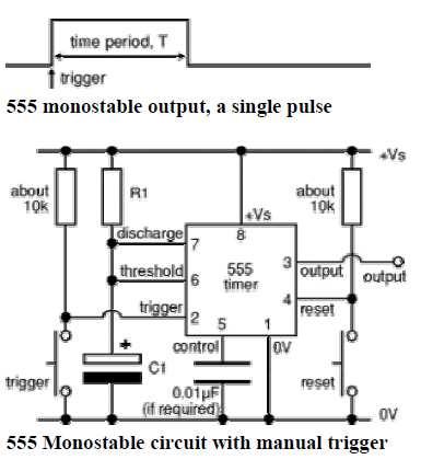
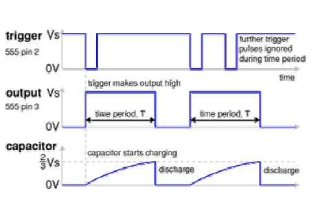
50 EXPERIMENT # 16 MONOSTABLE OPERATION OF 555 TIMER OBJECTIVE: To investigate the operation of 555 timer in the Mono-Stable mode APPARATUS: LM 555 RESISTORS CAPACITORS DC POWER SUPLLY DIGITAL MULTIMETER OSCILLOSCOPE OPERATION: A Mono-stable circuit produces a single output pulse when triggered. It is called a Monostable because it is stable in just one state: 'output low'. The 'output high' state is temporary. The duration of the pulse is called the time period (T) and this is determined by resistor R1 and capacitor C1: time period, T = 1.1 R1 C1 T = time period in seconds (s) R1 = resistance in ohms (Ω) C1 = capacitance in farads (F) The maximum reliable time period is about 10 minutes. Why 1.1? The capacitor charges to 2/3 = 67% so it is a bit longer than the time constant (R1 C1) which is the time taken to charge to 63%. Choose C1 first (there are relatively few values available). Choose R1 to give the time period you need. R1 should be in the range 1k to 1M, so use a fixed resistor of at least 1k in series if R1 is variable. Beware that electrolytic capacitor values are not accurate; errors of at least 20% are common. Beware that electrolytic capacitors leak charge which substantially increases the time period if you are using a high value resistor - use the formula as only a very rough guide! For example the Timer Project should have a maximum time period of 266s (about 4½ minutes), but many electrolytic capacitors extend this to about 10 minutes! The timing period is triggered (started) when the trigger input (555 pin 2) is less than 1/3 Vs, this makes the output high (Vs) and the capacitor C1 starts to charge through resistor R1. Once the time period has started further trigger pulses are ignored. The threshold input (555 pin 6) monitors the voltage across C1 and when this reaches 2/3 Vs the time period is over and the output becomes low. At the same time discharge (555 pin 7) is connected to 0V, discharging the capacitor ready for the next trigger. The reset input (555 pin 4) overrides all other inputs and the timing may be cancelled at any time by connecting reset to 0V, this instantly makes the output low and discharges the capacitor. If the reset function is not required the reset pin should be connected to Vs. ELECTRONICS-II 50
51 ELECTRONICS-II 51
 a push switch as shown in the diagram.")

52 Power-on reset or trigger: It may be useful to ensure that a mono-stable circuit is reset or triggered automatically when the power supply is connected or switched on. This is achieved by using a capacitor instead of (or in addition to) a push switch as shown in the diagram. The capacitor takes a short time to charge, briefly holding the input close to 0V when the circuit is switched on. A switch may be connected in parallel with the capacitor if manual operation is also required. This arrangement is used for the trigger in the Timer Project. Edge-triggering: If the trigger input is still less than 1/3 Vs at the end of the time period the output will remain high until the trigger is greater than 1/3 Vs. This situation can occur if the input signal is from an on-off switch or sensor. The Mono-stable can be made edge triggered, responding only to changes of an input signal, by connecting the trigger signal through a capacitor to the trigger input. The capacitor passes sudden changes (AC) but blocks a constant (DC) signal. For further information please see the page on capacitance. The circuit is 'negative edge triggered' because it responds to a sudden fall in the input signal. The resistor between the trigger (555 pin 2) and Vs ensures that the trigger is normally high (Vs). OBSERVATIONS: Teacher s Signature:. Date:. Teacher s Name: Engr Saqib Riaz. ELECTRONICS-II 52
Federal Urdu University of Arts, Science & Technology Islamabad Pakistan THIRD SEMESTER ELECTRONICS - II BASIC ELECTRICAL & ELECTRONICS LAB
 THIRD SEMESTER ELECTRONICS - II BASIC ELECTRICAL & ELECTRONICS LAB DEPARTMENT OF ELECTRICAL ENGINEERING Prepared By: Checked By: Approved By: Engr. Saqib Riaz Engr. M.Nasim Khan Dr.Noman Jafri Lecturer
Government Polytechnic Muzaffarpur Name of the Lab: Applied Electronics Lab
 Government Polytechnic Muzaffarpur Name of the Lab: Applied Electronics Lab Subject Code: 1620408 Experiment-1 Aim: To obtain the characteristics of field effect transistor (FET). Theory: The Field Effect
Facility of Engineering. Biomedical Engineering Department. Medical Electronic Lab BME (317) Post-lab Forms
 Post-lab Forms") Facility of Engineering Biomedical Engineering Department Medical Electronic Lab BME (317) Post-lab Forms Prepared by Eng.Hala Amari Spring 2014 Facility of Engineering Biomedical Engineering Department
Facility of Engineering Biomedical Engineering Department Medical Electronic Lab BME (317) Post-lab Forms Prepared by Eng.Hala Amari Spring 2014 Facility of Engineering Biomedical Engineering Department
CHARACTERIZATION OF OP-AMP
 EXPERIMENT 4 CHARACTERIZATION OF OP-AMP OBJECTIVES 1. To sketch and briefly explain an operational amplifier circuit symbol and identify all terminals. 2. To list the amplifier stages in a typical op-amp
Objective: To study and verify the functionality of a) PN junction diode in forward bias. Sl.No. Name Quantity Name Quantity 1 Diode
 PN junction diode in forward bias. Sl.No. Name Quantity Name Quantity 1 Diode") Experiment No: 1 Diode Characteristics Objective: To study and verify the functionality of a) PN junction diode in forward bias Components/ Equipments Required: b) Point-Contact diode in reverse bias Components
Experiment No: 1 Diode Characteristics Objective: To study and verify the functionality of a) PN junction diode in forward bias Components/ Equipments Required: b) Point-Contact diode in reverse bias Components
Linear IC s and applications
 Questions and Solutions PART-A Unit-1 INTRODUCTION TO OP-AMPS 1. Explain data acquisition system Jan13 DATA ACQUISITION SYSYTEM BLOCK DIAGRAM: Input stage Intermediate stage Level shifting stage Output
Concepts to be Reviewed
 Introductory Medical Device Prototyping Analog Circuits Part 3 Operational Amplifiers, http://saliterman.umn.edu/ Department of Biomedical Engineering, University of Minnesota Concepts to be Reviewed Operational
EXPERIMENT NO -9 TRANSITOR COMMON -BASE CONFIGURATION CHARACTERISTICS
 Contents EXPERIMENT NO -9 TRANSITOR COMMON -BASE CONFIGURATION CHARACTERISTICS... 3 EXPERIMENT NO -10. FET CHARACTERISTICS... 8 Experiment # 11 Non-inverting amplifier... 13 Experiment #11(B) Inverting
LIC & COMMUNICATION LAB MANUAL
 LIC & Communication Lab Manual LIC & COMMUNICATION LAB MANUAL FOR V SEMESTER B.E (E& ( E&C) (For private circulation only) NAME: DEPARTMENT OF ELECTRONICS & COMMUNICATION SRI SIDDHARTHA INSTITUTE OF TECHNOLOGY
GATE SOLVED PAPER - IN
 YEAR 202 ONE MARK Q. The i-v characteristics of the diode in the circuit given below are : v -. A v 0.7 V i 500 07 $ = * 0 A, v < 0.7 V The current in the circuit is (A) 0 ma (C) 6.67 ma (B) 9.3 ma (D)
Dev Bhoomi Institute Of Technology Department of Electronics and Communication Engineering PRACTICAL INSTRUCTION SHEET
 Dev Bhoomi Institute Of Technology Department of Electronics and Communication Engineering PRACTICAL INSTRUCTION SHEET LABORATORY MANUAL EXPERIMENT NO. ISSUE NO. : ISSUE DATE: REV. NO. : REV. DATE : PAGE:
LINEAR IC APPLICATIONS
 1 B.Tech III Year I Semester (R09) Regular & Supplementary Examinations December/January 2013/14 1 (a) Why is R e in an emitter-coupled differential amplifier replaced by a constant current source? (b)
Electronic Circuits II - Revision
 Electronic Circuits II - Revision -1 / 16 - T & F # 1 A bypass capacitor in a CE amplifier decreases the voltage gain. 2 If RC in a CE amplifier is increased, the voltage gain is reduced. 3 4 5 The load
ECEN Network Analysis Section 3. Laboratory Manual
 ECEN 3714----Network Analysis Section 3 Laboratory Manual LAB 07: Active Low Pass Filter Oklahoma State University School of Electrical and Computer Engineering. Section 3 Laboratory manual - 1 - Spring
Shankersinh Vaghela Bapu Institute of Technology INDEX
 Shankersinh Vaghela Bapu Institute of Technology Diploma EE Semester III 3330905: ELECTRONIC COMPONENTS AND CIRCUITS INDEX Sr. No. Title Page Date Sign Grade 1 Obtain I-V characteristic of Diode. 2 To
For input: Peak to peak amplitude of the input = volts. Time period for 1 full cycle = sec
 Inverting amplifier: [Closed Loop Configuration] Design: A CL = V o /V in = - R f / R in ; Assume R in = ; Gain = ; Circuit Diagram: RF +10V F.G ~ + Rin 2 3 7 IC741 + 4 6 v0-10v CRO Model Graph Inverting
Difference between BJTs and FETs. Junction Field Effect Transistors (JFET)
") Difference between BJTs and FETs Transistors can be categorized according to their structure, and two of the more commonly known transistor structures, are the BJT and FET. The comparison between BJTs
Difference between BJTs and FETs Transistors can be categorized according to their structure, and two of the more commonly known transistor structures, are the BJT and FET. The comparison between BJTs
LM2900 LM3900 LM3301 Quad Amplifiers
 LM2900 LM3900 LM3301 Quad Amplifiers General Description The LM2900 series consists of four independent dual input internally compensated amplifiers which were designed specifically to operate off of a
Facility of Engineering. Biomedical Engineering Department. Medical Electronic Lab BME (317) Pre-Report Forms
 Pre-Report Forms") Facility of Engineering Biomedical Engineering Department Medical Electronic Lab BME (317) Pre-Report Forms Prepared by Eng.Hala Amari Spring 2014 Facility of Engineering Biomedical Engineering Department
Facility of Engineering Biomedical Engineering Department Medical Electronic Lab BME (317) Pre-Report Forms Prepared by Eng.Hala Amari Spring 2014 Facility of Engineering Biomedical Engineering Department
Federal Urdu University of Arts, Science & Technology Islamabad Pakistan SECOND SEMESTER ELECTRONICS - I
 SECOND SEMESTER ELECTRONICS - I BASIC ELECTRICAL & ELECTRONICS LAB DEPARTMENT OF ELECTRICAL ENGINEERING Prepared By: Checked By: Approved By: Engr. Yousaf Hameed Engr. M.Nasim Khan Dr.Noman Jafri Lecturer
ENEE307 Lab 7 MOS Transistors 2: Small Signal Amplifiers and Digital Circuits
 ENEE307 Lab 7 MOS Transistors 2: Small Signal Amplifiers and Digital Circuits In this lab, we will be looking at ac signals with MOSFET circuits and digital electronics. The experiments will be performed
Op-Amp Simulation Part II
 Op-Amp Simulation Part II EE/CS 5720/6720 This assignment continues the simulation and characterization of a simple operational amplifier. Turn in a copy of this assignment with answers in the appropriate
UNIT - 1 OPERATIONAL AMPLIFIER FUNDAMENTALS
 UNIT - 1 OPERATIONAL AMPLIFIER FUNDAMENTALS 1.1 Basic operational amplifier circuit- hte basic circuit of an operational amplifier is as shown in above fig. has a differential amplifier input stage and
LF442 Dual Low Power JFET Input Operational Amplifier
 LF442 Dual Low Power JFET Input Operational Amplifier General Description The LF442 dual low power operational amplifiers provide many of the same AC characteristics as the industry standard LM1458 while
UNIVERSITY OF NORTH CAROLINA AT CHARLOTTE Department of Electrical and Computer Engineering
 UNIVERSITY OF NORTH CAROLINA AT CHARLOTTE Department of Electrical and Computer Engineering EXPERIMENT 5 GAIN-BANDWIDTH PRODUCT AND SLEW RATE OBJECTIVES In this experiment the student will explore two
INTEGRATED CIRCUITS AND APPLICATIONS LAB MANUAL
 INTEGRATED CIRCUITS AND APPLICATIONS LAB MANUAL V SEMESTER Department of Electronics and communication Engineering Government Engineering College, Dahod-389151 http://www.gecdahod.ac.in/ L A B M A N U
LM13600 Dual Operational Transconductance Amplifiers with Linearizing Diodes and Buffers
 LM13600 Dual Operational Transconductance Amplifiers with Linearizing Diodes and Buffers General Description The LM13600 series consists of two current controlled transconductance amplifiers each with
Amplifier Frequency Response, Feedback, Oscillations; Op-Amp Block Diagram and Gain-Bandwidth Product
 Amplifier Frequency Response, Feedback, Oscillations; Op-Amp Block Diagram and Gain-Bandwidth Product Physics116A,12/4/06 Draft Rev. 1, 12/12/06 D. Pellett 2 Negative Feedback and Voltage Amplifier AB
ASTABLE MULTIVIBRATOR
 555 TIMER ASTABLE MULTIIBRATOR MONOSTABLE MULTIIBRATOR 555 TIMER PHYSICS (LAB MANUAL) PHYSICS (LAB MANUAL) 555 TIMER Introduction The 555 timer is an integrated circuit (chip) implementing a variety of
Analog Circuit II Laboratory ( EC 409) EC 409 Analog Electronics Lab - II
 EC 409 Analog Electronics Lab - II") Analog Circuit II Laboratory ( EC 409) Subject Subject Title L T P Contact Credit Full Code Hours / Unit# Marks EC 409 Analog Electronics Lab - II 0 0 2 2 1 100 Course Outcomes:- After successful completion
Analog Circuit II Laboratory ( EC 409) Subject Subject Title L T P Contact Credit Full Code Hours / Unit# Marks EC 409 Analog Electronics Lab - II 0 0 2 2 1 100 Course Outcomes:- After successful completion
Department of Biomedical Engineering BME 317. Medical Electronics Lab
 Department of Biomedical Engineering BME 317 Medical Electronics Lab Modified by Dr.Husam AL.Hamad and Eng.Roba AL.Omari Summer 2009 Exp # Title Page 1 2 3 4 An Introduction To Basic Laboratory Equipments
ELECTRONIC DEVICES AND CIRCUITS LABORATORY MANUAL FOR II / IV B.E (EEE): I - SEMESTER
: I - SEMESTER") ELECTRONIC DEVICES AND CIRCUITS LABORATORY MANUAL FOR II / IV B.E (EEE): I - SEMESTER DEPT. OF ELECTRICAL AND ELECTRONICS ENGINEERING SIR C.R.REDDY COLLEGE OF ENGINEERING ELURU 534 007 ELECTRONIC DEVICES
ELECTRONIC DEVICES AND CIRCUITS LABORATORY MANUAL FOR II / IV B.E (EEE): I - SEMESTER DEPT. OF ELECTRICAL AND ELECTRONICS ENGINEERING SIR C.R.REDDY COLLEGE OF ENGINEERING ELURU 534 007 ELECTRONIC DEVICES
CHARACTERISTICS OF OPERATIONAL AMPLIFIERS - I
 CHARACTERISTICS OF OPERATIONAL AMPLIFIERS - I OBJECTIVE The purpose of the experiment is to examine non-ideal characteristics of an operational amplifier. The characteristics that are investigated include
Lab 2: Discrete BJT Op-Amps (Part I)
") Lab 2: Discrete BJT Op-Amps (Part I) This is a three-week laboratory. You are required to write only one lab report for all parts of this experiment. 1.0. INTRODUCTION In this lab, we will introduce and
Lab 2: Discrete BJT Op-Amps (Part I) This is a three-week laboratory. You are required to write only one lab report for all parts of this experiment. 1.0. INTRODUCTION In this lab, we will introduce and
LABORATORY #3 QUARTZ CRYSTAL OSCILLATOR DESIGN
 LABORATORY #3 QUARTZ CRYSTAL OSCILLATOR DESIGN OBJECTIVES 1. To design and DC bias the JFET transistor oscillator for a 9.545 MHz sinusoidal signal. 2. To simulate JFET transistor oscillator using MicroCap
Electronics Lab. (EE21338)
") Princess Sumaya University for Technology The King Abdullah II School for Engineering Electrical Engineering Department Electronics Lab. (EE21338) Prepared By: Eng. Eyad Al-Kouz October, 2012 Table of
Princess Sumaya University for Technology The King Abdullah II School for Engineering Electrical Engineering Department Electronics Lab. (EE21338) Prepared By: Eng. Eyad Al-Kouz October, 2012 Table of
Phy 335, Unit 4 Transistors and transistor circuits (part one)
") Mini-lecture topics (multiple lectures): Phy 335, Unit 4 Transistors and transistor circuits (part one) p-n junctions re-visited How does a bipolar transistor works; analogy with a valve Basic circuit
Mini-lecture topics (multiple lectures): Phy 335, Unit 4 Transistors and transistor circuits (part one) p-n junctions re-visited How does a bipolar transistor works; analogy with a valve Basic circuit
FACTFILE: GCSE Technology and Design
 FACTFILE: GCSE Technology and Design OPTION A: ELECTRONIC AND MICROELECTRONIC CONTROL SYSTEMS 2.14 Timers Astable Learning Outcomes You should be able to: demonstrate knowledge and understanding of the
UNIVERSITY OF NORTH CAROLINA AT CHARLOTTE Department of Electrical and Computer Engineering
 UNIVERSITY OF NORTH CAROLINA AT CHARLOTTE Department of Electrical and Computer Engineering EXPERIMENT 8 MOSFET AMPLIFIER CONFIGURATIONS AND INPUT/OUTPUT IMPEDANCE OBJECTIVES The purpose of this experiment
Lab 9: Operational amplifiers II (version 1.5)
") Lab 9: Operational amplifiers II (version 1.5) WARNING: Use electrical test equipment with care! Always double-check connections before applying power. Look for short circuits, which can quickly destroy
Lab 9: Operational amplifiers II (version 1.5) WARNING: Use electrical test equipment with care! Always double-check connections before applying power. Look for short circuits, which can quickly destroy
4.2.2 Metal Oxide Semiconductor Field Effect Transistor (MOSFET)
") 4.2.2 Metal Oxide Semiconductor Field Effect Transistor (MOSFET) The Metal Oxide Semitonductor Field Effect Transistor (MOSFET) has two modes of operation, the depletion mode, and the enhancement mode.
4.2.2 Metal Oxide Semiconductor Field Effect Transistor (MOSFET) The Metal Oxide Semitonductor Field Effect Transistor (MOSFET) has two modes of operation, the depletion mode, and the enhancement mode.
Chapter 8: Field Effect Transistors
 Chapter 8: Field Effect Transistors Transistors are different from the basic electronic elements in that they have three terminals. Consequently, we need more parameters to describe their behavior than
CHARACTERISTICS OF OPERATIONAL AMPLIFIERS - II
 CHARACTERISTICS OF OPERATIONAL AMPLIFIERS - II OBJECTIVE The purpose of the experiment is to examine non-ideal characteristics of an operational amplifier. The characteristics that are investigated include
EE 3305 Lab I Revised July 18, 2003
 Operational Amplifiers Operational amplifiers are high-gain amplifiers with a similar general description typified by the most famous example, the LM741. The LM741 is used for many amplifier varieties
EE 210 Lab Exercise #5: OP-AMPS I
 EE 210 Lab Exercise #5: OP-AMPS I ITEMS REQUIRED EE210 crate, DMM, EE210 parts kit, T-connector, 50Ω terminator, Breadboard Lab report due at the ASSIGNMENT beginning of the next lab period Data and results
Third Year (Electrical & Telecommunication Engineering)
") Z PRACTICAL WORK BOOK For The Course EE-315 Electric Filter For Third Year (Electrical & Telecommunication Engineering) Name of Student: Class: Batch : Discipline: Class Roll No.: Examination Seat No.
Z PRACTICAL WORK BOOK For The Course EE-315 Electric Filter For Third Year (Electrical & Telecommunication Engineering) Name of Student: Class: Batch : Discipline: Class Roll No.: Examination Seat No.
GATE: Electronics MCQs (Practice Test 1 of 13)
") GATE: Electronics MCQs (Practice Test 1 of 13) 1. Removing bypass capacitor across the emitter leg resistor in a CE amplifier causes a. increase in current gain b. decrease in current gain c. increase
GATE: Electronics MCQs (Practice Test 1 of 13) 1. Removing bypass capacitor across the emitter leg resistor in a CE amplifier causes a. increase in current gain b. decrease in current gain c. increase
CHADALAWADA RAMANAMMA ENGINEERING COLLEGE (AUTONOMOUS) Chadalawada Nagar, Renigunta Road, Tirupati
 Chadalawada Nagar, Renigunta Road, Tirupati") ELECTRONIC DEVICES AND CIRCUITS LABORATORY MANUAL Subject Code : 17CA04305 Regulations : R17 Class : III Semester (ECE) CHADALAWADA RAMANAMMA ENGINEERING COLLEGE (AUTONOMOUS) Chadalawada Nagar, Renigunta
ELECTRONIC DEVICES AND CIRCUITS LABORATORY MANUAL Subject Code : 17CA04305 Regulations : R17 Class : III Semester (ECE) CHADALAWADA RAMANAMMA ENGINEERING COLLEGE (AUTONOMOUS) Chadalawada Nagar, Renigunta
Dimensions in inches (mm) .268 (6.81).255 (6.48) .390 (9.91).379 (9.63) .045 (1.14).030 (.76) 4 Typ. Figure 1. Typical application circuit.
 .268 (6.81).255 (6.48) .390 (9.91).379 (9.63) .045 (1.14).030 (.76) 4 Typ. Figure 1. Typical application circuit.") LINEAR OPTOCOUPLER FEATURES Couples AC and DC signals.% Servo Linearity Wide Bandwidth, > KHz High Gain Stability, ±.%/C Low Input-Output Capacitance Low Power Consumption, < mw Isolation Test Voltage,
LINEAR OPTOCOUPLER FEATURES Couples AC and DC signals.% Servo Linearity Wide Bandwidth, > KHz High Gain Stability, ±.%/C Low Input-Output Capacitance Low Power Consumption, < mw Isolation Test Voltage,
ENGR4300 Test 3A Fall 2002
 1. 555 Timer (20 points) Figure 1: 555 Timer Circuit For the 555 timer circuit in Figure 1, find the following values for R1 = 1K, R2 = 2K, C1 = 0.1uF. Show all work. a) (4 points) T1: b) (4 points) T2:
University of North Carolina, Charlotte Department of Electrical and Computer Engineering ECGR 3157 EE Design II Fall 2009
 University of North Carolina, Charlotte Department of Electrical and Computer Engineering ECGR 3157 EE Design II Fall 2009 Lab 1 Power Amplifier Circuits Issued August 25, 2009 Due: September 11, 2009
DEPARTMENT OF ELECTRICAL ENGINEERING AND COMPUTER SCIENCE MASSACHUSETTS INSTITUTE OF TECHNOLOGY CAMBRIDGE, MASSACHUSETTS 02139
 DEPARTMENT OF ELECTRICAL ENGINEERING AND COMPUTER SCIENCE MASSACHUSETTS INSTITUTE OF TECHNOLOGY CAMBRIDGE, MASSACHUSETTS 019.101 Introductory Analog Electronics Laboratory Laboratory No. READING ASSIGNMENT
NJM324C. Low power quad operational amplifiers
 Low power quad operational amplifiers Features Wide gain bandwidth:.mhz typ. Input common-mode voltage range includes ground Large voltage gain:db typ. Very low supply current per amplifier:ua typ. Low
hij Teacher Resource Bank GCE Electronics Exemplar Examination Questions ELEC2 Further Electronics
 hij Teacher Resource Bank GCE Electronics Exemplar Examination Questions ELEC2 Further Electronics The Assessment and Qualifications Alliance (AQA) is a company limited by guarantee registered in England
Practical Manual. Deptt.of Electronics &Communication Engg. (ECE)
") Practical Manual LAB: BASICS OF ELECTRONICS 1 ST SEM.(CSE/CV) Deptt.of Electronics &Communication Engg. (ECE) RAO PAHALD SINGH GROUP OF INSTITUTIONS BALANA(MOHINDER GARH)12302 Prepared By. Mr.SANDEEP KUMAR
Practical Manual LAB: BASICS OF ELECTRONICS 1 ST SEM.(CSE/CV) Deptt.of Electronics &Communication Engg. (ECE) RAO PAHALD SINGH GROUP OF INSTITUTIONS BALANA(MOHINDER GARH)12302 Prepared By. Mr.SANDEEP KUMAR
Başkent University Department of Electrical and Electronics Engineering EEM 214 Electronics I Experiment 9
 Başkent University Department of Electrical and Electronics Engineering EEM 214 Electronics I Experiment 9 COMMON-COLLECTOR (EMITTER FOLLOWER) AMPLIFIER Aim: 1. To measure the open-circuit voltage gain,
EE 230 Lab Lab 9. Prior to Lab
 MOS transistor characteristics This week we look at some MOS transistor characteristics and circuits. Most of the measurements will be done with our usual lab equipment, but we will also use the parameter
CIRCUIT DIAGRAM Half Wave Rectifier. Half Wave Rectifier with filter 2012/ODD/III/ECE/EC I/LM 1
 CIRCUIT DIAGRAM Half Wave Rectifier Half Wave Rectifier with filter 2012/ODD/III/ECE/EC I/LM 1 Ex.No. 1 Date: / /2012 Power supply circuit using Half Wave rectifiers AIM To Build and understand the operation
Lecture (03) The JFET
 The JFET") Lecture (03) The JFET By: Dr. Ahmed ElShafee ١ JFET Basic Structure Figure shows the basic structure of an n channel JFET (junction field effect transistor). Wire leads are connected to each end of the
Lecture (03) The JFET By: Dr. Ahmed ElShafee ١ JFET Basic Structure Figure shows the basic structure of an n channel JFET (junction field effect transistor). Wire leads are connected to each end of the
Analog Circuits Part 3 Operational Amplifiers
 Introductory Medical Device Prototyping Analog Circuits Part 3 Operational Amplifiers, http://saliterman.umn.edu/ Department of Biomedical Engineering, University of Minnesota Concepts to be Reviewed Operational
Assist Lecturer: Marwa Maki. Active Filters
 Active Filters In past lecture we noticed that the main disadvantage of Passive Filters is that the amplitude of the output signals is less than that of the input signals, i.e., the gain is never greater
Chapter 10: Operational Amplifiers
 Chapter 10: Operational Amplifiers Differential Amplifier Differential amplifier has two identical transistors with two inputs and two outputs. 2 Differential Amplifier Differential amplifier has two identical
Lab 1 - Revisited. Oscilloscope demo IAP Lecture 2 1
 Lab 1 - Revisited Display signals on scope Measure the time, frequency, voltage visually and with the scope Voltage measurement* Build simple circuits on a protoboard.* Oscilloscope demo 6.091 IAP Lecture
Homework Assignment 07
 Homework Assignment 07 Question 1 (Short Takes). 2 points each unless otherwise noted. 1. A single-pole op-amp has an open-loop low-frequency gain of A = 10 5 and an open loop, 3-dB frequency of 4 Hz.
Lecture 2 Analog circuits. Seeing the light..
 Lecture 2 Analog circuits Seeing the light.. I t IR light V1 9V +V IR detection Noise sources: Electrical (60Hz, 120Hz, 180Hz.) Other electrical IR from lights IR from cameras (autofocus) Visible light
ET Training. Electronics: JFET Instructor: H.Pham. The JUNCTION FIELF EFFECT TRANSISTOR (JFET) n channel JFET p channel JFET
 n channel JFET p channel JFET") The JUNCTION FIELF EFFECT TRANSISTOR (JFET) n channel JFET p channel JFET 1 The BIASED JFET VDD provides a drain-to-source voltage and supplies current from drain to source VGG sets the reverse-biased
The JUNCTION FIELF EFFECT TRANSISTOR (JFET) n channel JFET p channel JFET 1 The BIASED JFET VDD provides a drain-to-source voltage and supplies current from drain to source VGG sets the reverse-biased
Draw in the space below a possible arrangement for the resistor and capacitor. encapsulated components
 1). An encapsulated component is known to consist of a resistor and a capacitor. It has two input terminals and two output terminals. A 5V, 1kHz square wave signal is connected to the input terminals and
Quad Ground Sense Operational Amplifier. The CO324 is monolithic IC with four built-in operational amplifiers featuring internal phase compensation.
 The CO4 is monolithic IC with four built-in operational amplifiers featuring internal phase compensation. Either a dual or single power supply can be driven, and these products can be driven by a digital
NJM4151 V-F / F-V CONVERTOR
 V-F / F-V CONVERTOR GENERAL DESCRIPTION PACKAGE OUTLINE The NJM4151 provide a simple low-cost method of A/D conversion. They have all the inherent advantages of the voltage-to-frequency conversion technique.
Analog Electronic Circuits Lab-manual
 2014 Analog Electronic Circuits Lab-manual Prof. Dr Tahir Izhar University of Engineering & Technology LAHORE 1/09/2014 Contents Experiment-1:...4 Learning to use the multimeter for checking and indentifying
Experiments #6. Differential Amplifier
 Experiments #6 Differential Amplifier 1) Objectives: To understand the DC and AC operation of a differential amplifier. To measure DC voltages and currents in differential amplifier. To obtain measured
Introduction to Op Amps
 Introduction to Op Amps ENGI 242 ELEC 222 Basic Op-Amp The op-amp is a differential amplifier with a very high open loop gain 25k AVOL 500k (much higher for FET inputs) high input impedance 500kΩ ZIN 10MΩ
Linear electronic. Lecture No. 1
 1 Lecture No. 1 2 3 4 5 Lecture No. 2 6 7 8 9 10 11 Lecture No. 3 12 13 14 Lecture No. 4 Example: find Frequency response analysis for the circuit shown in figure below. Where R S =4kR B1 =8kR B2 =4k R
ECE 3274 MOSFET CD Amplifier Project
 ECE 3274 MOSFET CD Amplifier Project 1. Objective This project will show the biasing, gain, frequency response, and impedance properties of the MOSFET common drain (CD) amplifier. 2. Components Qty Device
The MOSFET can be easily damaged by static electricity, so careful handling is important.
 ECE 3274 MOSFET CS Amplifier Project Richard Cooper 1. Objective This project will show the biasing, gain, frequency response, and impedance properties of the MOSFET common source (CS) amplifiers. 2. Components
Experiment EB2: IC Multivibrator Circuits
 EEE1026 Electronics II: Experiment Instruction Learning Outcomes Experiment EB2: IC Multivibrator Circuits LO1: Explain the principles and operation of amplifiers and switching circuits LO2: Analyze high
 Distributed by: www.jameco.com 1-800-831-4242 The content and copyrights of the attached material are the property of its owner. LM2900 LM3900 LM3301 Quad Amplifiers General Description The LM2900 series
To design/build monostable multivibrators using 555 IC and verify their operation using measurements by observing waveforms.
 AIM: SUBJECT: ANALOG ELECTRONICS (2130902) EXPERIMENT NO. 09 DATE : TITLE: TO DESIGN/BUILD MONOSTABLE MULTIVIBRATORS USING 555 IC AND VERIFY THEIR OPERATION USING MEASUREMENTS BY OBSERVING WAVEFORMS. DOC.
LM2904AH. Low-power, dual operational amplifier. Related products. Description. Features. See LM2904WH for enhanced ESD performances
 LM2904AH Low-power, dual operational amplifier Datasheet - production data Related products See LM2904WH for enhanced ESD performances Features Frequency compensation implemented internally Large DC voltage
Dev Bhoomi Institute Of Technology Department of Electronics and Communication Engineering PRACTICAL INSTRUCTION SHEET REV. NO. : REV.
 Dev Bhoomi Institute Of Technology Department of Electronics and Communication Engineering PRACTICAL INSTRUCTION SHEET LABORATORY MANUAL EXPERIMENT NO. ISSUE NO. : ISSUE DATE: July 200 REV. NO. : REV.
LF411 Low Offset, Low Drift JFET Input Operational Amplifier
 Low Offset, Low Drift JFET Input Operational Amplifier General Description These devices are low cost, high speed, JFET input operational amplifiers with very low input offset voltage and guaranteed input
Process Components. Process component
 What are PROCESS COMPONENTS? Input Transducer Process component Output Transducer The input transducer circuits are connected to PROCESS COMPONENTS. These components control the action of the OUTPUT components
ENGR 201 Homework, Fall 2018
 Chapter 1 Voltage, Current, Circuit Laws (Selected contents from Chapter 1-3 in the text book) 1. What are the following instruments? Draw lines to match them to their cables: Fig. 1-1 2. Complete the
Question Paper Code: 21398
 Reg. No. : Question Paper Code: 21398 B.E./B.Tech. DEGREE EXAMINATION, MAY/JUNE 2013 Fourth Semester Electrical and Electronics Engineering EE2254 LINEAR INTEGRATED CIRCUITS AND APPLICATIONS (Regulation
Unit WorkBook 4 Level 4 ENG U19 Electrical and Electronic Principles LO4 Digital & Analogue Electronics 2018 Unicourse Ltd. All Rights Reserved.
 Pearson BTEC Levels 4 Higher Nationals in Engineering (RQF) Unit 19: Electrical and Electronic Principles Unit Workbook 4 in a series of 4 for this unit Learning Outcome 4 Digital & Analogue Electronics
TL494M PULSE-WIDTH-MODULATION CONTROL CIRCUIT
 Complete PWM Power Control Circuitry Uncommitted Outputs for 00-mA Sink or Source Current Output Control Selects Single-Ended or Push-Pull Operation Internal Circuitry Prohibits Double Pulse at Either
AURORA S ENGINEERING COLLEGE BHONGIR, NALGONDA DIST
 AURORA S ENGINEERING COLLEGE BHONGIR, NALGONDA DIST. 508116. Lab manual of IC APPLICATIONS LAB 3 rd Year 1 st Sem. ECE 2014-15 DEPARTMENT OF ELECTRONICS AND COMMUNICATION ENGINEERING 1 PREFACE Integrated
Lecture 2 Analog circuits. Seeing the light..
 Lecture 2 Analog circuits Seeing the light.. I t IR light V1 9V +V IR detection Noise sources: Electrical (60Hz, 120Hz, 180Hz.) Other electrical IR from lights IR from cameras (autofocus) Visible light
ECE 310L : LAB 9. Fall 2012 (Hay)
") ECE 310L : LAB 9 PRELAB ASSIGNMENT: Read the lab assignment in its entirety. 1. For the circuit shown in Figure 3, compute a value for R1 that will result in a 1N5230B zener diode current of approximately
ECE 310L : LAB 9 PRELAB ASSIGNMENT: Read the lab assignment in its entirety. 1. For the circuit shown in Figure 3, compute a value for R1 that will result in a 1N5230B zener diode current of approximately
Dual Operational Amplifiers
 FEATURES Wide range of supply voltages Low supply current drain independent of supply voltage Low input biasing current Low input offset voltage and offset current Input common-mode voltage range includes
Quad ground sense operational amplifier
 Quad ground sense operational amplifier BAA / BAAF / BAAFV The BAA, BAAF, and BAAFV are monolithic ICs with four built-in operational amplifiers featuring internal phase compensation. Either a dual or
ML4818 Phase Modulation/Soft Switching Controller
 Phase Modulation/Soft Switching Controller www.fairchildsemi.com Features Full bridge phase modulation zero voltage switching circuit with programmable ZV transition times Constant frequency operation
Operational Amplifiers: Part II
 1. Introduction Operational Amplifiers: Part II The name "operational amplifier" comes from this amplifier's ability to perform mathematical operations. Three good examples of this are the summing amplifier,
ANALOG ELECTRONIC CIRCUITS LABORATORY MANUAL (CODE: EEE - 228)
") ANALOG ELECTRONIC CIRCUITS LABORATORY MANUAL (CODE: EEE - 228) DEPARTMENT OF ELECTRONICS & COMMUNICATION ENGINEERING ANIL NEERUKONDA INSTITUTE OF TECHNOLOGY & SCIENCES (Affiliated to AU, Approved by AICTE
ANALOG ELECTRONIC CIRCUITS LABORATORY MANUAL (CODE: EEE - 228) DEPARTMENT OF ELECTRONICS & COMMUNICATION ENGINEERING ANIL NEERUKONDA INSTITUTE OF TECHNOLOGY & SCIENCES (Affiliated to AU, Approved by AICTE
B.E. SEMESTER III (ELECTRICAL) SUBJECT CODE: X30902 Subject Name: Analog & Digital Electronics
 SUBJECT CODE: X30902 Subject Name: Analog & Digital Electronics") B.E. SEMESTER III (ELECTRICAL) SUBJECT CODE: X30902 Subject Name: Analog & Digital Electronics Sr. No. Date TITLE To From Marks Sign 1 To verify the application of op-amp as an Inverting Amplifier 2 To
B.E. SEMESTER III (ELECTRICAL) SUBJECT CODE: X30902 Subject Name: Analog & Digital Electronics Sr. No. Date TITLE To From Marks Sign 1 To verify the application of op-amp as an Inverting Amplifier 2 To
Lab 2 Revisited Exercise
 Lab 2 Revisited Exercise +15V 100k 1K 2N2222 Wire up led display Note the ground leads LED orientation 6.091 IAP 2008 Lecture 3 1 Comparator, Oscillator +5 +15 1k 2 V- 7 6 Vin 3 V+ 4 V o Notice that power
ENGR4300 Test 4A Spring 2005
 Question 1 Diodes Assume that the forward bias threshold voltage for the diode in the circuit is 0.7V. A. Consider the following circuit a) What type of diode circuit is the circuit above? (1 pt) half
Experiment#: 8. The JFET Characteristics & DC Biasing. Electronics (I) Laboratory. The Hashemite University. Faculty of Engineering
 Laboratory. The Hashemite University. Faculty of Engineering") The Hashemite University Faculty of Engineering Department of Electrical and Computer Engineering Electronics (I) Laboratory Experiment#: 8 The JFET Characteristics & DC Biasing Student s Name : Ja'afar
The Hashemite University Faculty of Engineering Department of Electrical and Computer Engineering Electronics (I) Laboratory Experiment#: 8 The JFET Characteristics & DC Biasing Student s Name : Ja'afar
Experiments #7. Operational Amplifier part 1
 Experiments #7 Operational Amplifier part 1 1) Objectives: The objective of this lab is to study operational amplifier (op amp) and its applications. We will be simulating and building some basic op-amp
ECE 363 FINAL (F16) 6 problems for 100 pts Problem #1: Fuel Pump Controller (18 pts)
 6 problems for 100 pts Problem #1: Fuel Pump Controller (18 pts)") ECE 363 FINAL (F16) NAME: 6 problems for 100 pts Problem #1: Fuel Pump Controller (18 pts) You are asked to design a high-side switch for a remotely operated fuel pump. You decide to use the IRF9520 power
ECE 363 FINAL (F16) NAME: 6 problems for 100 pts Problem #1: Fuel Pump Controller (18 pts) You are asked to design a high-side switch for a remotely operated fuel pump. You decide to use the IRF9520 power