Supertex inc. AN-H56. Designing An Ultrasound Pulser with MD1812/MD1813 Composite Drivers By Ching Chu, Sr. Application Engineer.
|
|
|
- Douglas Spencer
- 6 years ago
- Views:
Transcription
1 AN-H Application Note Designing An Ultrasound Pulser with MD8/MD8 Composite Drivers By Ching Chu, Sr. Application Engineer Introduction The MD8 and the MD8 are two unique composite return-to-zero (RTZ) pulser drivers for ultrasound applications. The ICs have built-in level shifters that provide negative P-MOS gate DC bias and fast AC coupled gate drive signals. They enable the fast damping functions necessary to generate return-to-zero bipolar pulses, and are also able to keep the zero-state to as long as needed, even to infinity. These kinds of fast return-to zero and DC coupled features are very useful for medical ultrasound imaging equipment, piezoelectric transducer drivers, material flaw detection, ultrasonic NDT detection, and sonar ranger applications, especially for those that need to launch ultrasound in pseudorandom codes. Designing a Pulser with the MD8/ This application note describes how to use MD8 or MD8 to design the basic channel of an ultrasound transmitter with the RTZ feature. The circuit is a single channel ultrasound transmitter using the MD8 or MD8 to drive TC0 & TC0 MOSFETs. It can generate fast return to zero waveforms. The output of high voltage to transducer has ±A source and sink current capability. A CPLD programmable logic circuit and on-board 0MHz crystal oscillator generate a fast logic signal to control the pulse circuit. The CPLD has a six-pin JTAG connection for Xilinx s USB or a convenient parallel-port programming link cable. The circuit consists of one MD8K or MD8K in a -lead xx0.9mm QFN package, driving TC0FGs and TC0FGs, two complementary high-voltage P and N- channel MOSFETs in one single SO-8 package. The input stage of the MD8/ is a high-speed level translator that is able to operate with logic input signals of.v to.0v amplitude. In this circuit, the CPLD output logic is typically.v. An adaptive threshold circuit is used with the pin inside of the MD8 to set the level translator threshold to the middle of the input logic 0 and logic levels. The pin serves a dual purpose. First, its logic level is used to compute the threshold voltage level for the channel input level translators. Second, when is low, the outputs are disabled, with the A and C outputs high and the B and D outputs low (for MD8 only). This assists in properly precharging the coupling capacitors that may be used in series in the gate drive circuit of external PMOS and NMOS FETs. The MD8/ level translator uses a proprietary composite drive circuit, which provides DC coupling, together with highspeed operation. The output pin, OUT C, is designed to drive the return-to-zero PMOS FET through a capacitor as fast as an AC coupling gate driver, and OUT G provides delayed DC coupling negative biased gate control to the same PMOS FET. The OUT C swings between V H and V L voltages, while OUT G is within V SS or V NEG levels. Note that the OUT C and OUT G pins of one chip are designed to drive together for one PMOS FET, and that the PMOS FET source is typically connected to the same potential of the MD8/ V SS voltage. Each of the output stages of OUT A, OUT B, OUT C & OUT D of MD8/ are capable of peak currents of up to ±.0A, depending on the supply voltages used and load capacitance. But a kω resistor, R, must be between OUT G and the gate of the PMOS FET, which is driven by the OUT C through a capacitor. This configuration provides the optimal series resistance value of the gate DC bias driver circuit. The output stage of the MD8/ has separate power connections enabling the output signal high and low levels to be chosen independently from the driver supply voltages. As an example, the input logic levels may be 0V and.8v, the control logic may be powered by +V and V, and the output high and low levels may be varied anywhere over the range of +V to -V. In this design example, MD8/ s V DD and V H are both powered by +0V, V SS and V L are grounded, and V NEG is 0V. The source pin of the RTZ PMOS FET driven by the OUT C and OUT G pins is connected to ground. PCB Layout Techniques It is very important that the slab at the bottom of the IC package, which is the IC substrate pin, be externally connected to the V NEG pin to make sure it always has the lowest potential in any condition. Doc.# DSAN-AN-H A00
2 Use high-speed PCB trace design practices that are compatible with the circuit s operating speed. The internal circuitry of the MD8/ can operate at up to 00MHz, with the primary speed limitation being due to load capacitance. Because of this high speed and the high transient currents that result when driving capacitive loads, the supply voltage bypass capacitors should be as close to the supply pins as possible. The V SS and V L pins should have low inductance feed-through connections that are connected directly to a solid ground plane. If these voltages are not zero, they will require bypass capacitors similar to the positive power supplies. The V DD supplies determine the output logic levels. These two pins can draw fast transient currents of up to.0a, so they should be provided with a low-impedance bypass capacitor at the chip s pins. A ceramic capacitor of up to.0µf may be appropriate. Minimize the trace length to the ground plane, and insert a ferrite bead in the power supply lead to the capacitor to prevent resonance in the power supply lines. A common voltage source and local decoupling capacitor may be used for the V DD pins, which should always have the same DC level applied to them. For applications that are sensitive to jitter and noise, insert another ferrite bead between V DD and decouple each pin separately. Pay particular attention to minimizing trace lengths and using sufficient trace width to reduce inductance. Surface mount components are highly recommended. Since the output impedance of this driver is very low, in some cases it may be desirable to add a small value resistor in series with the output to obtain better waveform integrity at the load terminals. This will, of course, reduce the output voltage slew rate at the terminals of a capacitive load. Pay particular attention to the parasitic coupling from the driver s output to the input signal terminals. This feedback may cause oscillations or spurious waveform shapes on the edges of signal transitions. Since the input operates with signals down to.v, even small coupling voltages may cause problems. Use of a solid ground plane and good power and signal layout practices will prevent this problem. Also ensure that the circulating ground return current from a capacitive load cannot react with common inductance to create noise voltages in the input logic circuitry. Testing the Ultrasound Pulser The MD8 RTZ pulser design example is tested with the following power supply voltage and current limiting: 0 to +00V ma, 0 to -00V ma, V DD = +0V 0mA, V NEG -0V ma, V CC +.V, 90mA. AN-H The signal appears at the SMA connector J. There is a : attenuation of the signal, due to the value of resistor R. When driving a real transducer load, the value of this resistor should be reduced in value to match the load impedance. The signal passes through jumper J, which can be used to terminate the signal in a dummy load, comprising a 0pF capacitor in parallel with a kω resistor. When an external load is connected, the dummy load is not required, and J can be configured to pass the signals straight through to the output connector J. All the on-board test points are designed to work with an active oscilloscope probe, such as the Tektronix P MΩ active probe. Because TP is connected to the, where potentially damaging voltages could be present, make sure that / does not exceed the probe limit. If using another type of high impedance oscilloscope probe for the test points, ensure that the ground lead connections to the circuit board ground plane are as short as possible. There are multiple frequency and waveform combinations that can be selected as bipolar pulses, PW or CW waveforms. An external clock input can be used if the on-board 0MHzoscillator is disabled. The external trigger input can be used to synchronize the output waveforms. There are five push buttons for selecting demo waveform, frequency, phase, and MD8 chip enable functions. Color LEDs indicate the demo selection states. The CH output allows the monitoring of one of the inputs (IN A, IN B, IN C, IN D or O E ) of the MD8/ via the select button. The MD8 and the MD8 are very similar in function. The only differences between them are the control of the (MD8) vs VLL (MD8) pin and their logic functions. Please read their data sheets for the details. In this design example, the CPLD program is using an on-board solder jumper, R, to sense the difference and works accordingly. The example MD8/ pulser circuit schematic, detail signals definitions, and some measured waveforms are shown below. Doc.# DSAN-AN-H A00
3 AN-H Operating Supply Voltages Sym Parameter Min Typ Max Units V NEG Negative Drive Supply V V DD Positive Drive Supply. 0 V V CC Logic Supply.8..0 V TC0 HV Positive Supply 0-00 V TC0 HV Negative Supply V Current Consumption Sym Typ Units Condition I DD. ma V DD = V I H.0 ma V H = V I NEG.0 ma V NEG = -V I CC 0 ma V CC =.V I PP.0 ma = 00V I NN.0 ma = -00V Waveform C, 0MHz, 8 cycles Load: 0pF//k Clock, Signal, and Trigger Frequency Internal Clock (MHz) A OUT /B OUT Signal (MHz) Internal Trigger (Hz) External Trigger (Hz) > f ET > > f ET > > f ET > > f ET >... 0> f ET > > f ET > > f ET >8. Doc.# DSAN-AN-H A00
4 AN-H Pulser Circuit Schematic +.V JTAG +0V +0V +00V 0.µF 0.µF.0µF CH- EXCLK OSC CLKIN Waveform Generator CPLD IN A IN B IN C IN D +.V IN A IN B IN C IN D VDD LT VH OUT A OUT B OUT G OUT C OUT D 0nF 0nF.0K TC0-00V.0µF JP XDCR 0MHz EN WAVE FREQ SEL PHASE ENAB SENSE LED LED LED PWR ENA 0 = MD8 VSS VL VNEG -0V MD8 0.µF 0nF TC0 C L R L Waveform A Waveform B Waveform C Waveform D Note: The duty cycle of the PW burst is set about 0.% for limited power dissipation Note: The duty cycle of the PW burst is set about % at.0mhz for limited power dissipation. Doc.# DSAN-AN-H A00
5 MD8/ Reference Design AN-H TP0 VNEG U P TC0 N 8 TP VDD TP J R C0 0pF 00V R k TP8 W J XDCR + TP TP R TP9 k VPP VNN D8 B00- WAV FRE SEL ENABLE PHASE SENSE N.C. 0 9 TMS TDI TDO TCK ENA 8 PWR 9 LED 0 LED LED J EX = Low R k R k SW TP D YLW (+.8,.,.0V) 8 TESTA TESTB TESTC CLK 0 9 CH EXTRG U XC9XL_VQ C 0. SENSE=0:MD8 DA U MD8 VL FB VNEG R9 00 C 0n 00V TP0 C 0 V + VPP + TP R0 00 VNN EN 0MHz X OUT TP TP8 TP TP DB D0 MMBD00BRM U P TC0 N 8 C 0 V DB DA C 0 V C µ 00V J J C µ 00V D9 B00- J EXCLK J CH J9 EXTRG TP R 0 TP R k R 0 R k R0 0 C 0. D YLW D YLW D GRN D RED C 0. C9 0. C 0. C 0. R k R k R k R k R k TP9 TP R8 00 R8 00 C 0. J JTAG R k R k R k R8 k R9 00 R0 00 R 00 R 00 R 00 R 0 SW SW SW SW C 0. C 0. C 0. C8 0. TP R 00 TP R 00 C 0. VDD VSS FB C0 0. VDD VH FB OUTA OUTB R9 00 R 00 C 0n 00V C8 0n 00V TP TP TP C µ 00V C9 µ 00V C 0. LT VNEG OUTG OUTC OUTD SUB C 0. R 00 R k TP R 00 Doc.# DSAN-AN-H A00


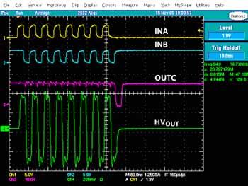
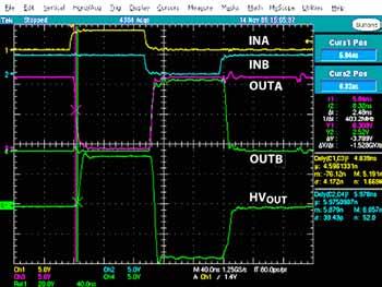
6 Fig. Waveform of.mhz Fig. Waveform of MHz AN-H Fig. Waveform of 0MHz Fig. Waveform of 0MHz Inverting Fig. Waveform of 0MHz 8 Cycles Fig. Waveform of mhz & Delay Readings Doc.# DSAN-AN-H A00
 AN-H Fig.")
 Doc.")
7 Fig. Waveform of 0MHz (at IN C, OUT C, OUT G, and P- Gate, V DD = V, V NEG = -0V) AN-H Fig. 8 Waveform of MHz (at IN C, OUT C, OUT G, and P- Gate, V DD = V, V NEG = -0V) Doc.# DSAN-AN-H A00
8 Board Connector and Test Pin Description CPLD Pin # Signal Description,, V LL Logic Power Supply +.V.,, Logic Power Ground 0V. AN-H WAV Selecting waveform pattern, push button input signal, Active low. See Fig. and Note. FRE Selecting frequency: 0,0,,.,. and 0.MHz button input signal, active low. SEL Selecting waveform to CH of oscilloscope, push button input signal, active low. ENABLE Enable button, Active low, Control. PHASE Button for output waveform phase control. IN A Output signal to MD8. 8 IN B Output signal to MD8. 9 IN C Output signal of MD8. 0 IN D Output signal of MD8. Output signal to MD8. LED Output signal LED, Yellow. LED Output signal LED, Yellow. 0 LED Output signal LED, Yellow. 8 ENA Output signal LED, RED, indicates = Hi. 9 PWR Output signal LED, Green, indicates power supply ok. 0 TMS Test Mode Select of JTAG. 9 TDI Test Data In of JTAG. TDO Test Data Out of JTAG. TCK Test Clock of JTAG. CLK CPLD clock input. 0 CH Output signal to CH of oscilloscope, select one of the output signal: IN A, IN B, IN C, IN D. 9 EXTRG External trigger signal input to control waveform timing. SENSE Sense solder jumper pin for MD8 = Hi or MD8 = Low, manufacture installation only. N.C. Reserved for manufacture test only. TEST_A Test pin reserved. TEST_B Test pin reserved. 8 TEST_C Test pin reserved. Doc.# DSAN-AN-H A00 8
9 AN-H Board Connector and Test Pin Description JTAG Connector Pin Number Signal Description J8- TMS Test Mode Select of CPLD J8- TDI Test Data In of CPLD J8- TDO Test Data Out of CPLD J8- TCK Test Clock of CPLD J8- Logic Power Supply Ground 0V for programming only J8- V CC Logic Power Supply +.V for programming only Signal / Jumper Pin Number Signal Description J EXCLK External clock input when on-board oscillator is disabled, or output the clock when it is enabled. J9 EXTRG External trigger signal input J CH CH waveform output signal to oscilloscope or other test equipment, CMOS logic level J XDCR MD8 / TC0s switching waveform output, to user load and/or oscilloscope, high voltage 0 to +/-00V J OSC_EN Jumper for on-board oscillator enable / disable, open = enabled, short = disable J Load JP Jumper for on-board RC load to MD8 high voltage output and XDCR connector R Jumper Solder jumper open if MD8 in installed, short to if MD8 is installed Low Voltage Supply Connector Pin Number Signal Description J- V CC +.V logic voltage supply for V CC (for CPLD only) J- V NEG -.0 to -V negative bias supply for V NEG and SUB J- Power supply ground J- Power supply ground J- V DD +0V positive driver voltage supply for V DD J- V DD +0V positive driver voltage supply for V DD High Voltage Supply Connector Pin Number Signal Description J- 0 to +00V positive high voltage supply with current limiting maximum to.0ma J- High voltage power supply return, 0V J- 0 to -00V Negative high voltage supply with current limiting maximum to.0ma does not recommend the use of its products in life support applications, and will not knowingly sell them for use in such applications unless it receives an adequate product liability indemnification insurance agreement. does not assume responsibility for use of devices described, and limits its liability to the replacement of the devices determined defective due to workmanship. No responsibility is assumed for possible omissions and inaccuracies. Circuitry and specifications are subject to change without notice. For the latest product specifications refer to the (website: http//) 0 All rights reserved. Unauthorized use or reproduction is prohibited. Doc.# DSAN-AN-H A00 9 Bordeaux Drive, Sunnyvale, CA 9089 Tel:
150V, 1.5A, Unipolar Ultrasound Pulser Demoboard +5.0V VLL AVDD PWR VSS VDD VPP CWD VDD VDD VDD. Q[7:0] Data Latch. Shift Register D0 SDI SUB VSUB
![150V, 1.5A, Unipolar Ultrasound Pulser Demoboard +5.0V VLL AVDD PWR VSS VDD VPP CWD VDD VDD VDD. Q[7:0] Data Latch. Shift Register D0 SDI SUB VSUB](/thumbs/88/116190510.jpg "150V, 1.5A, Unipolar Ultrasound Pulser Demoboard +5.0V VLL AVDD PWR VSS VDD VPP CWD VDD VDD VDD. Q[7:0] Data Latch. Shift Register D0 SDI SUB VSUB") 5V,.5A, Unipolar Ultrasound Pulser Demoboard General Description The HV755 is a monolithic eight-channel, high-speed, high voltage, unipolar ultrasound transmitter pulser. This integrated, high performance
5V,.5A, Unipolar Ultrasound Pulser Demoboard General Description The HV755 is a monolithic eight-channel, high-speed, high voltage, unipolar ultrasound transmitter pulser. This integrated, high performance
Supertex inc. MD1822DB3. MD TC8220: Three Level High Speed ±100V 3.0A Pulser Demoboard. Waveform Generator CPLD.
 MD8 + TC8: Three Level High Speed ±V.A Pulser Demoboard MD8DB Demoboard Features Ultrasound high voltage & high current RTZ pulser MD8 driving TC8 with two pairs of MOSFETs -level voltage pulse waveform
Supertex inc. MD1213DB1 MD TC6320 Demoboard High Speed ±100V 2A Pulser. Block Diagram TC6320 MD1213. Demoboard Features. General Description
 MDDB MD + TC0 Demoboard High Speed ±00V A Pulser General Description The MDDB can drive a transducer as a single channel transmitter for ultrasound and other applications. The demoboard consists of one
High Voltage Pulser Circuits By Ching Chu, Sr. Applications Engineer
 High Voltage Circuits By Ching Chu, Sr. Applications Engineer AN-H53 Application Note Introduction The high voltage pulser circuit shown in Figure 1 utilizes s complementary P- and N-channel transistors
Supertex inc. MD1210. High Speed Dual MOSFET Driver. Supertex MD1210. Features. General Description. Applications. Typical Application Circuit
 Supertex inc. MD0 High Speed Dual MOSFET Driver Features 6ns rise and fall time with 000pF load.0a peak output source/sink current.v to 5.0V input CMOS compatible 4.5V to 3V single positive supply voltage
Supertex inc. HV748DB1 HV748 ±75V 1.25A Ultrasound Pulser Demoboard
 HV78DB HV78 ±75V.5A Ultrasound Pulser Demoboard Introduction The HV78 is a monolithic -channel, high speed, high voltage, ultrasound transmitter pulser. This integrated, high performance circuit is in
HV739 ±100V 3.0A Ultrasound Pulser Demo Board
 HV79 ±00V.0A Ultrasound Pulser Demo Board HV79DB Introduction The HV79 is a monolithic single channel, high-speed, high voltage, ultrasound transmitter pulser. This integrated, high performance circuit
High Speed ±100V 2A Integrated Ultrasound Pulser Demo Board
 Introduction High Speed ±0V A Integrated Ultrasound Pulser Demo Board The HV7 is a complete, high-speed, high voltage, ultrasound tramitter pulser. This integrated high performance circuit is in a single
150V, 1.5A, Unipolar Ultrasound Pulser Demoboard +5.0V VLL AVDD PWR VSS VDD VPP CWD VDD VDD VDD. Q[7:0] Data Latch. Shift Register D0 SDI SUB VSUB
![150V, 1.5A, Unipolar Ultrasound Pulser Demoboard +5.0V VLL AVDD PWR VSS VDD VPP CWD VDD VDD VDD. Q[7:0] Data Latch. Shift Register D0 SDI SUB VSUB](/thumbs/88/114913177.jpg "150V, 1.5A, Unipolar Ultrasound Pulser Demoboard +5.0V VLL AVDD PWR VSS VDD VPP CWD VDD VDD VDD. Q[7:0] Data Latch. Shift Register D0 SDI SUB VSUB") HV755DB 5V,.5A, Unipolar Ultrasound Pulser Demoboard General Description The HV755 is a monolithic eight-channel, high-speed, high voltage, unipolar ultrasound transmitter pulser. This integrated, high
HV755DB 5V,.5A, Unipolar Ultrasound Pulser Demoboard General Description The HV755 is a monolithic eight-channel, high-speed, high voltage, unipolar ultrasound transmitter pulser. This integrated, high
High Speed Quad MOSFET Driver
 High Speed Quad MOSFET Driver Features General Description 6ns rise and fall time 2A peak output source/sink current.2v to 5V input CMOS compatible ±5V to ±2V supply voltage operation Smart Logic threshold
MD2130 Ultrasound Beamforming Transmitter Demoboard
 MD0DB MD0 Ultrasound Beamforming Transmitter Demoboard Introduction MD0 is a high-speed arbitrary waveform push-pull source-driver. It is designed for medical ultrasound imaging and HIFU beamforming applications.
Supertex inc. MD2131DB1. MD2131 Ultrasound Beamforming Transmitter Demoboard CPLD MD2131
 MD Ultrasound Beamforming Transmitter Demoboard Introduction The MD is a high speed, arbitrary waveform, push-pull source driver. It is designed for medical ultrasound imaging and HIFU beamforming applications.
Supertex inc. TC8220. Two Pair, N- and P-Channel Enhancement-Mode MOSFET. Features. General Description. Applications. Typical Application Circuit
 Supertex inc. TC8220 Two Pair, N- and P-Channel Enhancement-Mode MOSFET Features High voltage Vertical DMOS technology Integrated gate-to-source resistor Integrated gate-to-source Zener diode Low threshold,
Supertex inc. MD2134DB2. MD2134 Ultrasound Beamforming Transmitter Demoboard with Coupled Inductor CPLD MD2134
 MDDB MD Ultrasound Beamforming Transmitter Demoboard with Coupled Inductor Introduction The MD is a high speed, arbitrary waveform, push-pull source driver. It is designed for medical ultrasound imaging
Supertex inc. MD2131DB2. MD2131 Ultrasound Beamforming Transmitter Demoboard with Coupled Inductor CPLD MD2131
 MDDB MD Ultrasound Beamforming Transmitter Demoboard with Coupled Inductor Introduction The MD is a high speed, arbitrary waveform, push-pull source driver. It is designed for medical ultrasound imaging
Supertex inc. MD2134DB1. MD2134 Ultrasound Beamforming Transmitter Demoboard CPLD MD2134
 MD Ultrasound Beamforming Transmitter Demoboard Introduction The MD is a high-speed, arbitrary waveform, push-pull source-driver. It is designed for medical ultrasound imaging and HIFU beam forming applications.
High Speed, Integrated Ultrasound Driver IC +10V OUTPA1. 10nF OUTNA1. 10nF DV DD OUTPA2. 10nF OUTNA2. 10nF 48 AVSS -50V 0V OUTPA3 V SS OUTNA3 +10V
 Supertex inc. MD7 High Speed, Integrated Ultrasound Driver IC Features Drives two ultrasound transducer channels Generates five-level waveform Drives high voltage MOSFETs ±.0A source and sink peak current
Supertex inc. TC7920. Two Pair, N- and P-Channel Enhancement-Mode MOSFET with Drain-Diodes
 Two Pair, N- and P-Channel Enhancement-Mode MOSFET with Drain-Diodes Features High voltage Vertical DMOS technology Integrated drain output high voltage diodes Integrated gate-to-source resistor Integrated
High Speed ±100V 2A Integrated Ultrasound Pulser
 High Speed ±100V 2A Integrated Ultrasound Pulser Features HVCMOS technology for high performance 0 to ±100V output voltage ±2.0A source and sink current Built-in damping for RTZ waveform capability Gate-clamp
Four-Channel, High Speed, ±65V 750mA Ultrasound Pulser. General Description C2 C3 C4 VSUB. P-Driver. N-Driver. RGND 1 of 4 Channels GREF VNF HV738
 Supertex inc. HV738 Four-Channel, High Speed, ±65V 750mA Ultrasound Pulser Features HVCMOS technology for high performance High density integration ultrasound transmitter 0 to ±65V output voltage ±750mA
High-Voltage Switchmode Controllers with MOSFET
 HV91 HV912 HV913 High-Voltage Switchmode Controllers with MOSFET Ordering Information V IN Feedback Max MOSFET Switch Package Options Min Max Voltage Duty Cycle BV DSS R DS (ON) 14 Pin Plastic DIP 2 Pin
High-Voltage Current-Mode PWM Controller
 HV9112 High-Voltage Current-Mode PWM Controller Features 9. to 8V input voltage range Current-mode control High efficiency Up to 1.MHz internal oscillator Internal start-up circuit Low internal noise 5%
Low Charge Injection 32-Channel High Voltage Analog Switch. General Description. Level Shifters. Latches D LE CLR D LE CLR D LE CLR D LE CLR D LE CLR
 Low Charge Injection 32-Channel High Voltage Analog Switch Features 32-Channel high voltage analog switch 2:1 Multiplexer / emultiplexer 3.3V or 5.0V CMOS input logic level 20MHz data shift clock frequency
16-Channel Serial to Parallel Converter with High Voltage Backplane Driver and Push-Pull Outputs
 16-Channel Serial to Parallel Converter with High Voltage Backplane Driver and Push-Pull Outputs Features HVCMOS technology Output voltage up to +200V Shift register speed 500kHz @ V DD = 1.7V 16 high
High Voltage, Low Noise, Inductorless EL Lamp Driver. = 3.4V to 4.2V only) VDD HV850 REL GND 4 CLKIN CLKEN 5
 VDD HV850 REL GND 4 CLKIN CLKEN 5") Supertex inc. High Voltage, Low Noise, Inductorless Lamp Driver Features No external components required when using an external clock frequency frequency can be set by an external resistor Low noise DC
Supertex inc. High Voltage, Low Noise, Inductorless Lamp Driver Features No external components required when using an external clock frequency frequency can be set by an external resistor Low noise DC
8-Channel Serial to Parallel Converter with High Voltage Push-Pull Outputs, POL, Hi-Z, and Short Circuit Detect. General Description
 Features HVCMOS technology Operating output voltage of 250V Low power level shifting from 5.0 to 250V Shift register speed.0mhz @ V DD = 5.0V latch data outputs Output polarity and blanking Output short
Supertex inc. HV816. High Voltage, Dimmable EL Lamp Driver. Features. Applications. General Description
 Supertex inc. HV816 High Voltage, Dimmable EL Lamp Driver Features 360V PP output voltage for high brightness Large output load capability of up to 150nF 2.7 to 5.5V operating supply voltage Single lithium
High Speed, 200V, Full H-Bridge MOSFET Driver
 High Speed, 2V, Full H-Bridge MOSFET MD72 Features HVCMOS technology for high performance All N-MOSFET full-bridge driver Designed for 2V bridge supply voltage Up to.mhz operation frequency Greater than
Low Charge Injection 32-Channel High Voltage Analog Switch. General Description /V NN. Level Shifters. Latches D LE CLR D LE CLR D LE CLR D LE CLR
 Supertex inc. HV2801 Low Charge Injection 32-Channel High Voltage Analog Switch Features 32 Channels of high voltage analog switch 2:1 Multiplexer / emultiplexer 3.3V or 5.0V CMOS input logic level 30MHz
Supertex inc. HV Channel Serial To Parallel Converter With Open Drain Outputs. Features. General Description. Applications.
 Supertex inc. HV5523 32-Channel Serial To Parallel Converter With Open Drain Outputs Features Processed with HVCMOS technology Sink current minimum 00mA Shift register speed 6MHz Polarity and blanking
16-Channel Serial to Parallel Converter with High Voltage Backplane Driver and Push-Pull Outputs
 16-Channel Serial to Parallel Converter with High Voltage Backplane Driver and Push-Pull Outputs Features HVCMOS technology Output voltage up to +200V Shift register speed 500kHz @ = 2.0V 16 high voltage
Supertex inc. HV2661 Low Charge Injection 24-Channel High Voltage Analog Switch. General Description. Features. Applications.
 Low Charge Injection 24-Channel High Voltage Analog Switch Features 24 Channels of high voltage analog switch 3.3 or 5.0V CMOS input logic level 3:1 MUX-deMUX with 8 states 20MHz data shift clock frequency
TC7320 Six Pair, N- and P-Channel Enhancement-Mode MOSFET
 Six Pair, N- and P-Channel Enhancement-Mode MOSFET Features Six N- and P-channel MOSFET pairs Integrated gate-to-source resistor Integrated gate-to-source Zener diode Low threshold Low on-resistance Low
Supertex inc. HV9150DB1. Hysteretic DC/DC Controller Demoboard. General Description. Specifications. Board Layout. Supertex inc.
 HV90DB Hysteretic DC/DC Controller Demoboard General Description The Supertex HV90DB demoboard is for the evaluation of the HV90 hysteretic DC/DC controller. This demoboard consists of all necessary components
Supertex inc. AN-D26 Application Note High Voltage Isolated MOSFET Driver. Features
 Supertex inc. Features ND pplication Note High Voltage Isolated MOSFET Driver Switches up to ±00V from ground referenced logic Provides ±00V isolation between outputs No floating power supplies required
Supertex inc. LN V Cascoded N-Channel MOSFET L 100 YWLL
 Features 1200V breakdown voltage Low threshold, 1.V max. High input impedance Low input capacitance Integrated high voltage resistor divider Integrated 1000:1 resistor divider Compact 3x3 LFGA package
HV440DB2 Demo Board by Jimes Lei, Applications Engineering Manager
 Demo Board by Jimes Lei, Applications Engineering Manager Introduction The Supertex HV440 is a power-efficient, switch-mode ring generator IC requiring minimal external components. The demo board contains
Supertex inc. HV9910B. Universal High Brightness LED Driver. Features. General Description. Applications. Typical Application Circuit HV9910B
 Supertex inc. HV9910B Universal High Brightness LED Driver Features Switch mode controller for single switch LED drivers Enhanced drop-in replacement to the HV9910 Open loop peak current controller Internal
Supertex inc. HV7022C. 34-Channel Symmetric Row Driver. General Description. Features. Functional Block Diagram. Supertex inc.
 34-Channel Symmetric Row Driver Features HVCMOS technology Symmetric row drive (reduces latent imaging in ACTFEL displays) Output voltage up to +230V Low power level shifting Source/sink current minimum
Supertex inc. HV9150 HV9150. High Voltage Output Hysteretic Mode Step Up DC/DC Controller. Features. General Description. Applications.
 High Voltage Output Hysteretic Mode Step Up DC/DC Controller Features Wide output voltage range: 6V to 500V Low input voltage: 2.7V 5W maximum output power with external MOSFET driver Built-in charge pump
HV Channel, Low Harmonic Distortion, High Voltage Analog Switch with Bleed Resistors. General Description
 Supertex inc. HV2733 16-Channel, Low Harmonic istortion, Analog Switch with Bleed Resistors Features Low harmonic distortion Integrated bleed resistors on the outputs 3.3 or 5.5V CMOS input logic level
Dimmable, Low Noise, Dual EL Lamp Driver. 100µH Coilcraft LPS MΩ VREG VOUT LX CS 3 12 VDD EL1 2.0MΩ HV861K7-G. REL-Osc COM1 2. RSW-Osc.
 Supertex inc. HV86 Features Adjustable output regulation for dimming Lamp fade-in/fade-out capability Low audible noise 80V PP output voltage for higher brightness.v enable input logic high Single cell
HV9931 Unity Power Factor LED Lamp Driver
 Unity Power Factor LED Lamp Driver Features Constant output current Large step-down ratio Unity power factor Low input current harmonic distortion Fixed frequency or fixed off-time operation Internal 450V
Obsolete. Supertex inc. MD Channel Low-Noise Amplifier. General Description. Features. Applications. Typical Application Circuit
 Supertex inc. 4-Channel Low-oise Amplifier MD3880 Features 2.5 ± 0.125V operation 4 independent channels Fully differential inputs and outputs 0.74nV/ Hz input-referred noise at 18.5dB gain Ultra low current
Low Charge Injection 24-Channel SPST High Voltage Analog Switch with Bleed Resistors. Level Shifters. Latches D LE CLR D LE CLR D LE CLR D LE CLR
 Low Charge Injection 24-Channel SPST High Voltage nalog Switch with Bleed Resistors Features 24 Channels of high voltage analog switch Integrated bleed resistors on the outputs 3.3 or 5.0V CMOS input logic
Supertex inc. AN-H59. Application Note
 Supertex inc. AN-H Application Note High Voltage DC/DC Converter for Supertex Ultrasound Transmitter Demoboards By Afshaneh Brown, Applications Engineer, and Jimes Lei, Applications Manager Introduction
32-Channel High Voltage Amplifier Array
 32-Channel High Voltage Amplifier Array Features 32 independent high voltage amplifiers 3 operating voltage 295V output voltage 2.2V/µs typical output slew rate Adjustable output current source limit Adjustable
Supertex inc. HV264. Quad, High Voltage, Amplifier Array. Features. General Description. Applications. Block Diagram. Supertex inc.
 Quad, High Voltage, Amplifier Array Features Four independent high voltage amplifiers 190V output swing 9.0V/µs typical output slew rate Fixed gain of 66.7V/V High value internal feedback resistors Very
Supertex inc. HV2221. Low Charge Injection, 8-Channel, Unipolar, Negative High Voltage, Analog Switch. Features. General Description.
 Supertex inc. HV2221 Low Charge Injection, 8-Channel, Unipolar, Negative High Voltage, Analog Switch Features Low on-resistance, 14Ω max. HVCMOS technology for high performance 3.3 or 5.0V CMOS input logic
Supertex inc. HV7801 HV7801. High Side Current Monitor 8.0 to 450V Voltage Gain of 5. Features. General Description. Applications
 High Side Current Monitor 80 to 450V Voltage Gain of 5 Features Supply voltage 8V to 450V Voltage output device Typical gain 50±1% Max 500mV Fast rise and fall time, 700ns to 20µs Maximum quiescent current
Supertex inc. TP2510. P-Channel Enhancement-Mode Vertical DMOS FET TP5AW. Features. General Description. Applications. Ordering Information
 TP251 P-Channel Enhancement-Mode Vertical DMOS FET Features Low threshold (-2.4V max.) High input impedance Low input capacitance (125pF max.) Fast switching speeds Low on-resistance Free from secondary
24/48V Fan Driver/Controller With High-Side Drive
 24/48V Fan Driver/Controller With High-Side Drive Features High-side drive allows use of tachs Direct interface to host controller Noise-immune linear speed control 4-bit digital speed control Operates
Supertex inc. HV809. Off-Line, High Voltage EL Lamp Driver. Features. General Description. Applications. Block Diagram.
 Off-Line, High Voltage EL Lamp Driver Features Processed with HVCMOS technology Input voltage up to 200V DC 400V peak-to-peak output voltage Output load up to 30nF (00in 2 for 3.nF/in 2 lamp) djustable
64-Channel Serial to Parallel Converter With High Voltage Push-Pull Outputs
 64-Channel Serial to Parallel Converter With High Voltage Push-Pull Outputs Features Processed with HVCMOS technology Operating output voltages to 300V Low power level shifting from 5.0 to 300V Shift register
N- and P-Channel Enhancement-Mode Dual MOSFET
 N- and P-Channel Enhancement-Mode Dual MOSFET TC2320 Features Low threshold Low on-resistance Low input capacitance Fast switching speeds Freedom from secondary breakdown Low input and output leakage Independent,
Supertex inc. HV892 HV892. Inductorless Liquid Lens Driver. General Description. Features. Applications. Typical Application Circuit. Supertex inc.
 Inductorless Liquid Lens Driver Features Drives capacitive loads up to 200pF Programmable drive amplitude (compatible with 40V RMS to 60V RMS lenses) On-chip boost converter No external inductor I 2 C
Features. RAMP Feed Forward Ramp/ Volt Sec Clamp Reference & Isolation. Voltage-Mode Half-Bridge Converter CIrcuit
 MIC3838/3839 Flexible Push-Pull PWM Controller General Description The MIC3838 and MIC3839 are a family of complementary output push-pull PWM control ICs that feature high speed and low power consumption.
Supertex inc. TP2540. P-Channel Enhancement-Mode Vertical DMOS FET. Features. General Description. Applications. Ordering Information.
 Features Low threshold (-2.4V max.) High input impedance Low input capacitance (6pF typical) Fast switching speeds Low on-resistance Free from secondary breakdown Low input and output leakage Applications
Supertex inc. HV9971DB1. Isolated, Constant Current HV9971 LED Driver Demoboard. Board Layout and Connection Diagram.
 Isolated, Constant Current HV9971 LED Driver Demoboard Board Layout and Connection Diagram Terminals for Monitoring Bus Voltage - + V AC = + 180-265VAC = 18-24V - I OUT = 330mA Connections 1. Input Voltage:
3-Channel LED Array Driver IC
 -Channel LED Array Driver IC Features Integrated 00V, 5Ω (typ.) MOSFETs Programmable output current to 80mA per channel TTL compatible PWM dimming inputs -Phase synchronous operation Leading edge blanking
Supertex inc. TN0702. N-Channel Enhancement-Mode Vertical DMOS FET. Features
 TN72 Features Low threshold - 1.6V max. High input impedance Low input capacitance - 13pF typical Fast switching speeds Low on-resistance guaranteed at = 2, 3, and 5V Free from secondary breakdown Low
Supertex inc. HV825. High Voltage EL Lamp Driver IC. Features
 High Voltage EL Lamp Driver IC Features Processed with HVCMOS technology.0 to.6v operating supply voltage DC to C conversion Output load of typically up to 6.0nF djustable output lamp frequency djustable
Supertex inc. LR8 High Input Voltage, Adjustable 3-Terminal Linear Regulator Features General Description Applications Typical Application Circuit
 Supertex inc. High Input Voltage, Adjustable 3-Terminal Linear Regulator Features 13.2-45 input voltage range Adjustable 1.20-44 output regulation 5% output voltage tolerance Output current limiting 10µA
Supertex inc. TN0106. N-Channel Enhancement-Mode Vertical DMOS FET
 TN16 N-Channel Enhancement-Mode Vertical DMOS FET Features Low threshold - 2.V max. High input impedance Low input capacitance - 5pF typical Fast switching speeds Low on-resistance Free from secondary
Supertex inc. HV9910BDB3. Low Voltage, High Current, LED Driver Demoboard. General Description. Specifications. Connection Diagram.
 HV990BDB3 Low Voltage, High Current, LED Driver Demoboard General Description The HV990BDB3 demoboard is a high current LED driver designed to drive one LED or two LEDs in series at currents up to.0a from
Supertex inc. VN10K. N-Channel Enhancement-Mode Vertical DMOS FET. Features. General Description. Applications. Ordering Information.
 VN1K N-Channel Enhancement-Mode Vertical DMOS FET Features Free from secondary breakdown Low power drive requirement Ease of paralleling Low C ISS and fast switching speeds Excellent thermal stability
Low Charge Injection 8-Channel High Voltage Analog Switches with Bleed Resistors. Level Shifters. Latches D LE CL D LE CL D LE CL D LE CL D LE CL
 Low Charge Injection 8-Channel High Voltage Analog Switches with Bleed Resistors Features HVCMOS technology for high performance Very low quiescent power dissipation (10µA max.) Output on-resistance (22Ω
Features. Slope Comp Reference & Isolation
 MIC388/389 Push-Pull PWM Controller General Description The MIC388 and MIC389 are a family of complementary output push-pull PWM control ICs that feature high speed and low power consumption. The MIC388/9
Supertex inc. TP0610T. P-Channel Enhancement Mode Vertical DMOS FETs. Features. General Description. Applications. Ordering Information
 Supertex inc. P-Channel Enhancement Mode Vertical DMOS FETs Features High input impedance and high gain Low power drive requirement Ease of paralleling Low C ISS and fast switching speeds Excellent thermal
Supertex inc. VN0109. N-Channel Enhancement-Mode Vertical DMOS FET. Features. General Description. Applications. Ordering Information.
 VN19 N-Channel Enhancement-Mode Vertical DMOS FET Features Free from secondary breakdown Low power drive requirement Ease of paralleling Low C ISS and fast switching speeds Excellent thermal stability
High Input Voltage, Adjustable 3-Terminal Linear Regulator
 High Input Voltage, Adjustable 3-Terminal Linear Regulator Features 13.2 to 100V input voltage range Stable with output capacitor Adjustable 1.20 to 88V output regulation 5% reference voltage tolerance
High Input Voltage, Adjustable 3-Terminal Linear Regulator
 High Input Voltage, Adjustable 3-Terminal Linear Regulator Features 13.2-450V input voltage range Adjustable 1.20-440V output regulation 5% output voltage tolerance Output current limiting 10µA typical
32-Channel Serial To Parallel Converter With High Voltage Push-Pull Outputs
 HV9308 HV9408 Ordering Information 3-Channel Serial To Parallel Converter With High Voltage Push-Pull Outputs Package Options Device Recommended 44 J-Lead Dice in Operating Quad Plastic Waffle Pack V PP
Supertex inc. TN2510. N-Channel Enhancement-Mode Vertical DMOS FET. Features. General Description. Applications. Ordering Information.
 TN51 N-Channel Enhancement-Mode Vertical DMOS FET Features Low threshold (.V max.) High input impedance Low input capacitance (15pF max.) Fast switching speeds Low on-resistance Free from secondary breakdown
Supertex inc. AN-H37. HV440 High Voltage Ring Generator. Application Note. Ramp Generator. Error Amp and PWM HV440
 AN-H37 Application Note HV440 High Voltage Ring Generator by Jimes Lei, Applications Engineering Manager Introduction The Supertex HV440 is used for implementing a pulse width modulated high voltage ring
Supertex inc. HV Pin Hotswap, Inrush Current Limiter Controllers (Negative Supply Rail) Features. General Description.
 Features. General Description.") 3-Pin Hotswap, Inrush Current Limiter Controllers (Negative Supply Rail) Features Pass element is only external part No sense resistor required Auto-adapt to pass element Short circuit protection UV &
3-Pin Hotswap, Inrush Current Limiter Controllers (Negative Supply Rail) Features Pass element is only external part No sense resistor required Auto-adapt to pass element Short circuit protection UV &
12-Channel High Voltage Analog Switch
 12-Channel Analog Switch Features HVCMOS technology for high performance Operating voltage of up to 200V Output on-resistance typically 22Ω Integrated bleed resistors on the outputs 5.0V to 12.0V CMOS
BV /BV DS(ON) D(ON) DSS DGS
 D(ON) DSS DGS") TP61T P-Channel Enhancement-Mode Vertical DMOS FET Features High input impedance and high gain Low power drive requirement Ease of paralleling Low C ISS and fast switching speeds Excellent thermal stability
TP61T P-Channel Enhancement-Mode Vertical DMOS FET Features High input impedance and high gain Low power drive requirement Ease of paralleling Low C ISS and fast switching speeds Excellent thermal stability
Supertex inc. TP2104. P-Channel Enhancement-Mode Vertical DMOS FET. Features. General Description. Applications. Ordering Information.
 TP214 Features High input impedance and high gain Low power drive requirement Ease of paralleling Low C ISS and fast switching speeds Excellent thermal stability Integral source-drain diode Free from secondary
High Speed PWM Controller
 High Speed PWM Controller FEATURES Compatible with Voltage or Current Mode Topologies Practical Operation Switching Frequencies to 1MHz 50ns Propagation Delay to Output High Current Dual Totem Pole Outputs
Supertex inc. HV Channel Serial to Parallel Converter With High Voltage Push-Pull Outputs. General Description. Features.
 32-Channel Serial to Parallel Converter With High Voltage Push-Pull Outputs Features Processed with HVCMOS technology Output voltages up to 80V Low power level shifting Shift register speed 8.0MHz ed data
Supertex inc. MD0105. Four-Channel High Voltage Protection T/R Switch. Features. General Description. Applications. Typical Application Circuit +130V
 Four-Channel High Voltage Protection T/R Switch Features Up to ±30V input voltage protection Low on resistance - 5Ω typical Fast switching speed Four electrically isolated channels No external supplies
Supertex inc. AN-D26. High Voltage Isolated MOSFET Driver. Application Note. Features
 Features High Voltage Isolated MOSFET river Switches up to ±00V from ground referenced logic Provides ±00V isolation between outputs No floating power supplies required to bias MOSFETs Operates isolated
MIC4478/4479/4480. General Description. Features. Applications. Typical Application. 32V Low-Side Dual MOSFET Drivers
 32V Low-Side Dual MOSFET Drivers General Description The MIC4478, MIC4479, and MIC4480 are low-side dual MOSFET drivers are designed to switch N-channel enhancement type MOSFETs from TTL-compatible control
MIC915. Features. General Description. Applications. Ordering Information. Pin Configuration. Pin Description. Dual 135MHz Low-Power Op Amp
 MIC915 Dual 135MHz Low-Power Op Amp General Description The MIC915 is a high-speed, unity-gain stable operational amplifier. It provides a gain-bandwidth product of 135MHz with a very low, 2.4mA supply
Low Charge Injection, 8-Channel, Enhanced, High Voltage Analog Switch. General Description. Level Shifters. Latches D LE CL D LE CL D LE CL D LE CL
 Supertex inc. HV2201 Low Charge Injection, 8-Channel, Enhanced, High Voltage Analog Switch Features HVCMOS technology for high performance 8 Channels of high voltage analog switch 3.3 or 5.0V CMOS input
High Speed PWM Controller
 High Speed PWM Controller application INFO available FEATURES Compatible with Voltage or Current Mode Topologies Practical Operation Switching Frequencies to 1MHz 50ns Propagation Delay to Output High
Supertex inc. HV Channel Serial to Parallel Converter With Open Drain Outputs. Features. General Description. Functional Block Diagram
 Supertex inc. HV5522 32-Channel Serial to Parallel Converter With Open Drain Outputs Features General Description Processed with HVCMOS technology Sink current minimum 00mA Shift register speed 8.0MHz
Supertex inc. CL8801. Sequential Linear LED Driver CL8801 GND SET1 SET2 SET3 SET4. Features. General Description. Applications
 Sequential Linear LED Driver Features Minimal component count (base config: + 4 resistors + diode bridge) No magnetics, no capacitors Up to 3W output >5Lm/W using efficient LEDs 85-90% electrical efficiency
Supertex inc. HV9911DB2 Boost LED Driver Demoboard with 1:3000 Dimming Ratio and Excellent Current Regulation. Board Layout and Connection Diagram
 The is an LED driver capable of driving up to twenty 100mA LEDs in series from an input of 9-16V DC. The demoboard uses Supertex s HV9911 IC in a boost topology. The converter has a very good initial regulation,
Understanding MOSFET Data. Type of Channel N-Channel, or P-Channel. Design Supertex Family Number TO-243AA (SOT-89) Die
 Die") Understanding MOSFET Data Application Note The following outline explains how to read and use Supertex MOSFET data sheets. The approach is simple and care has been taken to avoid getting lost in a maze
Understanding MOSFET Data Application Note The following outline explains how to read and use Supertex MOSFET data sheets. The approach is simple and care has been taken to avoid getting lost in a maze
BV /BV DS(ON) D(ON) DSS DGS
 D(ON) DSS DGS") P-Channel Enhancement-Mode Vertical DMOS FETs VP216 Features Free from secondary breakdown Low power drive requirement Ease of paralleling Low C ISS and fast switching speeds Excellent thermal stability
P-Channel Enhancement-Mode Vertical DMOS FETs VP216 Features Free from secondary breakdown Low power drive requirement Ease of paralleling Low C ISS and fast switching speeds Excellent thermal stability
DSX DGS DS(ON) D(ON) (V)
 D(ON) (V)") N7 N-Channel Enhancement-Mode Vertical DMOS FETs Features Free from secondary breakdown Low power drive requirement Ease of paralleling Low C ISS and fast switching speeds Excellent thermal stability Integral
N7 N-Channel Enhancement-Mode Vertical DMOS FETs Features Free from secondary breakdown Low power drive requirement Ease of paralleling Low C ISS and fast switching speeds Excellent thermal stability Integral
Supertex inc. TN2640. N-Channel Enhancement-Mode Vertical DMOS FETs. Features
 TN264 Features Low threshold (2.V max.) High input impedance Low input capacitance Fast switching speeds Low on-resistance Free from secondary breakdown Low input and output leakage pplications Logic level
Supertex inc. TN0604. N-Channel Enhancement-Mode Vertical DMOS FET. Features. General Description. Applications. Ordering Information.
 TN64 N-Channel Enhancement-Mode ertical DMOS FET Features Low threshold (1.6 max.) High input impedance Low input capacitance (14pF typical) Fast switching speeds Low on-resistance Free from secondary
32-Channel Serial to Parallel Converter With High Voltage Push-Pull Outputs VPP. High Voltage. Level Translators & Push-Pull Output Buffers
 32-Channel Serial to Parallel Converter With High Voltage Push-Pull Outputs Features Processed with HVCMOS technology Low power level shifting Source/sink current minimum 20mA Shift register speed 8.0MHz
Inductorless, Dual Output Off-Line Regulators
 SR036 Demo Kit Available Inductorless, Dual Output Off-Line Regulators Features Accepts peak input voltages up to 700 Operates directly off of rectified 120 AC or 240 AC Integrated linear regulator Minimal
Low Charge Injection, 8-Channel, High Voltage, Enhanced Analog Switch with Bleed Resistors. Level Shifters. Latches D LE CL D LE CL D LE CL D LE CL
 Supertex inc. HV2301 Low Charge Injection, 8-Channel, High Voltage, Enhanced Analog Switch with Bleed Resistors Features HVCMOS technology for high performance Integrated bleed resistors on the outputs
Supertex inc. TN2106. N-Channel Enhancement-Mode Vertical DMOS FET. Features. General Description. Applications. Ordering Information.
 Features Free from secondary breakdown Low power drive requirement Ease of paralleling Low C ISS and fast switching speeds Excellent thermal stability Integral source-drain diode High input impedance and
Supertex inc. DN2540. N-Channel Depletion-Mode Vertical DMOS FETs. General Description. Features. Applications. Ordering Information
 Supertex inc. DN254 N-Channel Depletion-Mode Vertical DMOS FETs Features High input impedance Low input capacitance Fast switching speeds Low on-resistance Free from secondary breakdown Low input and output