Three-terminal experiments on Si-MgO tunneling structures
|
|
|
- Alexandrina Norman
- 5 years ago
- Views:
Transcription


1 Juliane Laurer AG Dr. Max Bougeard Mustermann Referat Kommunikation & Marketing Verwaltung Three-terminal experiments on Si-MgO tunneling structures SFB 689 C9: Spin Injection into Silicon Juliane Laurer AG Bougeard FAKULTÄT FÜR PHYSIK
2 Measurement configurations Non-local spin-valve geometry: Separation of charge and spin current No parasitic effects such as AMR Pure spin information BUT: Processing and measurement not easy since 29 only two groups reported on successful spin injection into silicon
3 Measurement configurations Non-local spin-valve geometry: Separation of charge and spin current No parasitic effects such as AMR Pure spin information BUT: Processing and measurement not easy since 29 only two groups reported on successful spin injection into silicon Three-terminal Hanle geometry: Only one tunnel contact for spin injection and detection No separation of charge and spin current & detector is biased Spin lifetimes are much longer than theoretically expected Debate on the origin of measured Hanle-like signals
4 Origin of 3T signal: competing models Group of R. Jansen: S. Sharma, et al. PRB 89, 7531 (214) Hanle effect due to spin injection into Si, but describing theory is incorrect Group of M. Tanaka: S. Sato, et al. APL 17, 3247 (215) Paramagnetic layer formed at ferromagnettunnel barrier interface Group of M. Yamamoto: T. Uemura, et al. APL 11, (212) Tunneling rates depend on external B-field Group of H. Jaffrès & A. Fert: M. Tran, et al. PRL 12, 3661 (29) Sequential tunneling via localized states in the tunnel barrier or at the interfaces Groups of H. Dery & F. Casanova: O. Txoperena, et al. PRL 113, (214) Magnetoresistance due to Pauli spin blockade in defect states in the tunnel barrier
5 Origin of 3T signal: competing models Group of R. Jansen: S. Sharma, et al. PRB 89, 7531 (214) Hanle effect due to spin injection into Si, but describing theory is incorrect Group of M. Tanaka: S. Sato, et al. APL 17, 3247 (215) Paramagnetic layer formed at ferromagnettunnel barrier interface Group of M. Yamamoto: T. Uemura, et al. APL 11, (212) Tunneling rates depend on external B-field Group of H. Jaffrès & A. Fert: M. Tran, et al. PRL 12, 3661 (29) Sequential tunneling via localized states in the tunnel barrier or at the interfaces Groups of H. Dery & F. Casanova: O. Txoperena, et al. PRL 113, (214) Magnetoresistance due to Pauli spin blockade in defect states in the tunnel barrier
6 Outline 1. Growth and characterization of epitaxial hybrid Si/MgO/Fe/Au tunnel junctions 2. Three-terminal experiments on epitaxial tunnel junctions


7 Sample growth in combined MBE system Vacuum channel connected Si/Ge- and metal-mbe Growth of hybrid stacks without breaking the vacuum Good interface control Possibility of epitaxial growth with single crystalline tunnel barriers
8 Epitaxial Si/MgO/Fe/Au-stacks Au Fe MgO n + -Si Si/MgO/Fe/Au Atomically flat Si-MgO and Fe-MgO interfaces Single crystalline MgO tunnel barrier MgO predominantly grows in MgO 11 direction on Si 11

9 Epitaxial Si/MgO/Fe/Au-stacks Au Fe MgO n + -Si Fe 1 Si 11 Epitaxial Si/MgO/Fe/Au-stack with pronounced four-fold in plane magnetic anisotropy Excellent material for Si-based spin injection experiments
10 Current (ma) 3T experiments on Si/MgO/Fe/Au T = 4.2 K Extraction Injection Voltage (V)
11 Current (ma) Voltage 3T (µv) 3T experiments on Si/MgO/Fe/Au T = 4.2 K Extraction 35 T = 4.2 K I=-4µA I=-2µA I= µa I= 5µA I= 2µA I= 4µA I= 6µA I= 8µA Injection Voltage (V) Several B dependent signals: 1 T < B < 2 T Rotation of magnetization out of plane Magnetic field (T)
12 Current (ma) Voltage 3T (µv) 3T experiments on Si/MgO/Fe/Au T = 4.2 K Extraction 35 T = 4.2 K I=-4µA I=-2µA I= µa I= 5µA I= 2µA I= 4µA I= 6µA I= 8µA Injection Voltage (V) Several B dependent signals: 1 T < B < 2 T Rotation of magnetization out of plane mt < B < 1 T Magnetoresistive background? Magnetic field (T)
13 Current (ma) Voltage 3T (µv) 3T experiments on Si/MgO/Fe/Au T = 4.2 K Extraction 35 T = 4.2 K I=-4µA I=-2µA I= µa I= 5µA I= 2µA I= 4µA I= 6µA I= 8µA Injection Voltage (V) Several B dependent signals: 1 T < B < 2 T Rotation of magnetization out of plane mt < B < 1 T Magnetoresistive background? Magnetic field (T) B < 7 mt R drops with increasing B Hanle signal?
14 Curent (ma) 3T experiments with ohmic contacts 1. T = 4.2 K Extraction Injection Voltage (V)
15 Curent (ma) Voltage 3T (µv) 3T experiments with ohmic contacts T = 4.2 K I = -15µA I = -5µA I = 2µA I = 2µA I = 5µA 4 1. T = 4.2 K Extraction Injection Voltage (V) Magnetic field (T) Ohmic contacts no ferromagnet involved and no sign of tunneling Weak quadratic background signal No evidence of Hanle-type signal around B =
16 Current (ma) Samples without ferromagnet.4 T = 4.2 K Extraction Injection Voltage (V)
 I = -25µA I = -2")
17 Current (ma) Voltage 3T(mV) Samples without ferromagnet T = 4.2 K Extraction Injection Voltage (V) T = 4.2 K Magnetic field (T) I = -25µA I = -2.5µA I = -.5µA I = 3µA I = 25µA I = 5µA I = 15µA Weak linear background signal, especially for current extraction Strong Hanle-like signal around B = with FWHM 7 mt BUT: no ferromagnet Signal does NOT originate from spin injection into Si channel
18 Voltage 3T (µv) Voltage 3T (µv) Comparison: Samples with & without Fe Hanle-like signal with same FWHM for both samples BUT: without Fe: R increases with increasing B with Fe: R decreases with increasing B Magnetoresistive effect from tunneling through MgO barrier? Si / MgO / Au I= -75µA I= -25µA I= -2.5µA I= -.5µA I= 3µA I= 25µA I= 5µA I= 15µA Si / MgO / Fe / Au I=-4µA I=-2µA I= µa I= 5µA I= 2µA I= 4µA I= 6µA I= 8µA Magnetic field (T)
19 Voltage 3T (µv) Voltage 3T (µv) Comparison: Samples with & without Fe Hanle-like signal with same FWHM for both samples BUT: without Fe: R increases with increasing B with Fe: R decreases with increasing B Magnetoresistive effect from tunneling through MgO barrier? Si / MgO / Au I= -75µA I= -25µA I= -2.5µA I= -.5µA I= 3µA I= 25µA I= 5µA I= 15µA B = Groups of H. Dery & F. Casanova: O. Txoperena, et al. PRL 113, (214) Magnetoresistance due to Pauli spin blockade in defect states in the tunnel barrier Si / MgO / Fe / Au I=-4µA I=-2µA I= µa I= 5µA I= 2µA I= 4µA I= 6µA I= 8µA Magnetic field (T)

 Magnetoresistance due to Pauli spin blockade in defect states in the tunnel barrier 35 3 25 2 15 1 5-5 -1 Si / MgO / Fe / Au I=-4µA I=-2µA I= µa I=")
20 Voltage 3T (µv) Voltage 3T (µv) Comparison: Samples with & without Fe Hanle-like signal with same FWHM for both samples BUT: without Fe: R increases with increasing B with Fe: R decreases with increasing B Magnetoresistive effect from tunneling through MgO barrier? Si / MgO / Au I= -75µA I= -25µA I= -2.5µA I= -.5µA I= 3µA I= 25µA I= 5µA I= 15µA B = B Groups of H. Dery & F. Casanova: O. Txoperena, et al. PRL 113, (214) Magnetoresistance due to Pauli spin blockade in defect states in the tunnel barrier Si / MgO / Fe / Au I=-4µA I=-2µA I= µa I= 5µA I= 2µA I= 4µA I= 6µA I= 8µA Magnetic field (T)
21 Voltage 3T (mv) Voltage 3T (µv) Samples without ferromagnet Temperature dependence Dependence on orientation of B B out of plane B 45 B in plane Injection: I = -1µA T = 4.2K Extraction I = 1µA Magnetic field (T) 5K 4K 3K 2K 1K 4K Magnetic field (T) Background decreases with increasing temperature Hanle-like signal vanishes at T 5 K Hanle-like signal is independent on orientation of external magnetic field
22 Voltage (µv) Voltage (µv) Summary and outlook Epitaxial Si/MgO/Fe/Au tunneling stacks single crystalline MgO tunnel barrier Pronounced fourfold magnetic anisotropy Three-terminal experiments with & without Fe layer Hanle-like signal only occurs if MgO tunnel barrier is involved Signal cannot only stem from injected spins in the Si channel Analogies to Pauli spin blockade model in defect states of MgO R211A2_13 Si / MgO / Au R29A4_4 Si / MgO / Fe / Au I= -75µA I= -25µA I= -2.5µA I= -.5µA I= 3µA I= 25µA I= 5µA I= 15µA I=-4µA I=-2µA I= µa I= 5µA I= 2µA I= 4µA I= 6µA I= 8µA Magnetic field (T) Juliane Laurer, AG Bougeard, Juliane.Laurer@ur.de

23 Voltage (µv) Voltage (µv) Summary and outlook Epitaxial Si/MgO/Fe/Au tunneling stacks single crystalline MgO tunnel barrier Pronounced fourfold magnetic anisotropy Three-terminal experiments with & without Fe layer Hanle-like signal only occurs if MgO tunnel barrier is involved Signal cannot only stem from injected spins in the Si channel Analogies to Pauli spin blockade model in defect states of MgO R211A2_13 Si / MgO / Au R29A4_4 Si / MgO / Fe / Au I= -75µA I= -25µA I= -2.5µA I= -.5µA I= 3µA I= 25µA I= 5µA I= 15µA I=-4µA I=-2µA I= µa I= 5µA I= 2µA I= 4µA I= 6µA I= 8µA Magnetic field (T) Outlook Non-local spin-valve and non-local Hanle measurements for pure spin information Juliane Laurer, AG Bougeard, Juliane.Laurer@ur.de


24 Acknowledgment AG Bougeard Prof. Dr. Dominique Bougeard Mareen Schäfer Michaela Trottmann Chair Weiss Prof. Dr. Dieter Weiss Dr. Mariusz Ciorga Chair Back Prof. Dr. Christian Back Prof. Dr. Josef Zweck Dr. Matthias Kronseder Markus Härtinger Thank you for your attention.
<1> Au(1)<11> Si(1)<1> MgO(1)<1> Fe(1)<11>")
25 RHEED pattern of Si/MgO/Fe/Au Si(1)<11> MgO(1)<11> Fe(1)<1> Au(1)<11> Si(1)<1> MgO(1)<1> Fe(1)<11> Au(1)<1>
26 Kerr signal (a. u.) Kerr signal (a. u.) MOKE measurements in plane easy axis Kerr signal out of plane Kerr signal Magnetic field (mt) Magnetic field (T) Along in plane easy axis: Coercive field H C.36 mt Out of plane, i.e. along hard axis: Saturation at B 2.1 T


27 Epitaxial Si/MgO/Fe/Au-stacks Au Fe Si 11 MgO MgO 1 MgO 11 n + -Si Si/MgO/Fe/Au Very sharp and atomically flat interfaces MgO predominantly grows in MgO 11 direction on Si 11 BUT: observation of both, MgO 11 and MgO 1
28 Voltage 3T (µv) Voltage 3T (mv) Samples with ferromagnet Temperature dependence Dependence on orientation of B Extraction: I = -8µA T = 4.2K B out of plane B 45 B in plane Magnetic field (T) 4.2K 4K 5K 7K 1K 13K 15K 175K Magnetif field (T) Hanle-like signal present at least up to T = 175 K Strength of background signal decreases In-plane magnetic anisotropy comes into play Hanle-like signal might still be present in plane
29 V 3T (µv) R (k ) 3T comparison to Txoperena µA -5µA -2µA -5µA -3µA -1µA -,5µA µa R 3T ( ) R R = dv/di R = V(B=)/I magnetic field (T) V B=T (mv)
30 Voltage (µv) Voltage (µv) V NL (µv) V NL (µv) Voltage (µv) V NL (µv) V NL (µv) Voltage (µv) V NL (µv) V NL (µv) Non-local spin-valve experiments 5 Extraction Injection I = 3 µa T = 4.3 K magnetic field (T) R241A2_6 Extraction Inj 4, Det 7-1 I=2µA I=-2µA Inj 7, Det I=4µA I=-4µA 75 1 Inj 6, Det I=6µA I=-6µA Inj 7, Det 6 Det 4 Det 6 Det magnetic field (T) magnetic field (T) Inj 4, Det Inj 6, Det magnetic field (T)


")

")
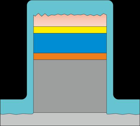
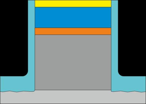

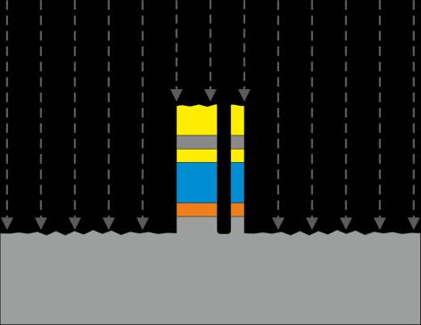
31 Mesa etching with channel isolation Au MgO Fe n + -Si Ion beam etching (IBE, Ar ions) Reactive ion etching (RIE, SF 6 + Ar) Al 2 O 3 deposition (ALD) Lift-off
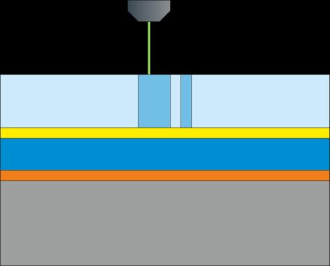


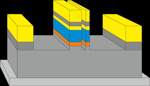


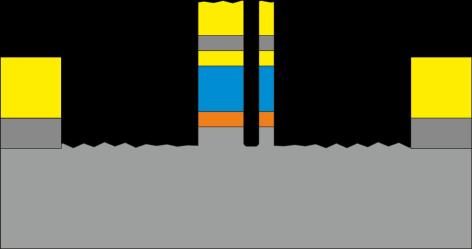
32 Processing steps on the mesa E-beam lithography Ti/Au evaporation IBE RIE (SF 6 + CHF 3 ) HF dip Ti/Au evaporation

33 Epitaxy and lattice mismatch
Supplementary Figure 1 High-resolution transmission electron micrograph of the
 Supplementary Figure 1 High-resolution transmission electron micrograph of the LAO/STO structure. LAO/STO interface indicated by the dotted line was atomically sharp and dislocation-free. Supplementary
SUPPLEMENTARY INFORMATION
 SUPPLEMENTARY INFORMATION doi:10.1038/nature11293 1. Formation of (111)B polar surface on Si(111) for selective-area growth of InGaAs nanowires on Si. Conventional III-V nanowires (NWs) tend to grow in
Supplementary information for Stretchable photonic crystal cavity with
 Supplementary information for Stretchable photonic crystal cavity with wide frequency tunability Chun L. Yu, 1,, Hyunwoo Kim, 1, Nathalie de Leon, 1,2 Ian W. Frank, 3 Jacob T. Robinson, 1,! Murray McCutcheon,
High-Speed Scalable Silicon-MoS 2 P-N Heterojunction Photodetectors
 High-Speed Scalable Silicon-MoS 2 P-N Heterojunction Photodetectors Veerendra Dhyani 1, and Samaresh Das 1* 1 Centre for Applied Research in Electronics, Indian Institute of Technology Delhi, New Delhi-110016,
MgO MTJ biosensors for immunomagnetic lateralflow
 MgO MTJ biosensors for immunomagnetic lateralflow detection Ricardo Jorge Penelas Janeiro Under supervision of Susana Isabel Pinheiro Cardoso de Freitas Dep. Physics, IST, Lisbon, Portugal Octrober 15,
SUPPLEMENTARY INFORMATION
 Induction of coherent magnetization switching in a few atomic layers of FeCo using voltage pulses Yoichi Shiota 1, Takayuki Nozaki 1, 2,, Frédéric Bonell 1, Shinichi Murakami 1,2, Teruya Shinjo 1, and
Compact size 3D magnetometer based on magnetoresistive sensors
 Compact size 3D magnetometer based on magnetoresistive sensors Gabriel António Nunes Farinha Under supervision of Prof. Susana Freitas Instituto de Engenharia de Sistemas e Computadores, Microsistemas
Progress toward a thousandfold reduction in 1/ f noise in magnetic sensors using an ac microelectromechanical system flux concentrator invited
 Progress toward a thousandfold reduction in 1/ f noise in magnetic sensors using an ac microelectromechanical system flux concentrator invited A. S. Edelstein a and G. A. Fischer U.S. Army Research Laboratory,
Nano-structured superconducting single-photon detector
 Nano-structured superconducting single-photon detector G. Gol'tsman *a, A. Korneev a,v. Izbenko a, K. Smirnov a, P. Kouminov a, B. Voronov a, A. Verevkin b, J. Zhang b, A. Pearlman b, W. Slysz b, and R.
HDD Technology Trends
 R e s e a r c h HDD Technology Trends Dr. Richard New Director of Research Hitachi Global Storage Technologies HDD Technology Challenges Storage Technology Capabilities Storage Usage Requirements Storage
Wu Lu Department of Electrical and Computer Engineering and Microelectronics Laboratory, University of Illinois, Urbana, Illinois 61801
 Comparative study of self-aligned and nonself-aligned SiGe p-metal oxide semiconductor modulation-doped field effect transistors with nanometer gate lengths Wu Lu Department of Electrical and Computer
Integration of III-V heterostructure tunnel FETs on Si using Template Assisted Selective Epitaxy (TASE)
") Integration of III-V heterostructure tunnel FETs on Si using Template Assisted Selective Epitaxy (TASE) K. Moselund 1, D. Cutaia 1. M. Borg 1, H. Schmid 1, S. Sant 2, A. Schenk 2 and H. Riel 1 1 IBM Research
Integration of III-V heterostructure tunnel FETs on Si using Template Assisted Selective Epitaxy (TASE) K. Moselund 1, D. Cutaia 1. M. Borg 1, H. Schmid 1, S. Sant 2, A. Schenk 2 and H. Riel 1 1 IBM Research
Magnetic tunnel junction sensors with conetic alloy. Lei, ZQ; Li, GJ; Egelhoff Jr, WF; Lai, PT; Pong, PWT
 Title Magnetic tunnel junction sensors with conetic alloy Author(s) Lei, ZQ; Li, GJ; Egelhoff Jr, WF; Lai, PT; Pong, PWT Citation The 2010 Asia-Pacific Data Storage Conference (APDSC'10), Hualien, Taiwan,
Spin-Precession Organic Magnetic Sensor
 Final Report 26 September 2012 Spin-Precession Organic Magnetic Sensor SRI Project P19028 ONR Contract N00014-09-C-0292 Prepared by: Srini Krishnamurthy, Senior Principal Scientist Applied Physical Sciences
Magnetic and Electromagnetic Microsystems. 4. Example: magnetic read/write head
 Magnetic and Electromagnetic Microsystems 1. Magnetic Sensors 2. Magnetic Actuators 3. Electromagnetic Sensors 4. Example: magnetic read/write head (C) Andrei Sazonov 2005, 2006 1 Magnetic microsystems
Magnetic Spin Devices: 7 Years From Lab To Product. Jim Daughton, NVE Corporation. Symposium X, MRS 2004 Fall Meeting
 Magnetic Spin Devices: 7 Years From Lab To Product Jim Daughton, NVE Corporation Symposium X, MRS 2004 Fall Meeting Boston, MA December 1, 2004 Outline of Presentation Early Discoveries - 1988 to 1995
Hybrid Group IV Nanophotonic Structures. Incorporating Diamond Silicon-Vacancy Color
 Hybrid Group IV Nanophotonic Structures Incorporating Diamond Silicon-Vacancy Color Centers Jingyuan Linda Zhang, Hitoshi Ishiwata 2,3, Thomas M. Babinec, Marina Radulaski, Kai Müller, Konstantinos G.
SUPPLEMENTARY INFORMATION
 SUPPLEMENTARY INFORMATION doi: 10.1038/nmat797 Spin injection/detection via an organic-based magnetic semiconductor Jung-Woo Yoo 1,, Chia-Yi Chen 3, H. W. Jang 4, C. W. Bark 4, V. N. Prigodin 1, C. B.
Vertical field effect transistors realized by cleaved-edge overgrowth
 Version date: 03.09.2001 Final version Paper number: C031178 Vertical field effect transistors realized by cleaved-edge overgrowth F. Ertl a, T. Asperger a, R. A. Deutschmann a, W. Wegscheider a,b, M.
NOVEL CHIP GEOMETRIES FOR THz SCHOTTKY DIODES
 Page 404 NOVEL CHIP GEOMETRIES FOR THz SCHOTTKY DIODES W. M. Kelly, Farran Technology Ltd., Cork, Ireland S. Mackenzie and P. Maaskant, National Microelectronics Research Centre, University College, Cork,
Machine-Aligned Fabrication of Submicron SIS Tunnel Junctions Using a Focused Ion Beam
 Machine-Aligned Fabrication of Submicron SIS Tunnel Junctions Using a Focused Ion Beam Robert. B. Bass, Jian. Z. Zhang and Aurthur. W. Lichtenberger Department of Electrical Engineering, University of
Magnetic tunnel junction sensor development for industrial applications
 Magnetic tunnel junction sensor development for industrial applications Introduction Magnetic tunnel junctions (MTJs) are a new class of thin film device which was first successfully fabricated in the
Supporting Information. Vertical Graphene-Base Hot-Electron Transistor
 Supporting Information Vertical Graphene-Base Hot-Electron Transistor Caifu Zeng, Emil B. Song, Minsheng Wang, Sejoon Lee, Carlos M. Torres Jr., Jianshi Tang, Bruce H. Weiller, and Kang L. Wang Department
InGaAs MOSFETs for CMOS:
 InGaAs MOSFETs for CMOS: Recent Advances in Process Technology J. A. del Alamo, D. Antoniadis, A. Guo, D.-H. Kim 1, T.-W. Kim 2, J. Lin, W. Lu, A. Vardi and X. Zhao Microsystems Technology Laboratories,
High-Ohmic Resistors using Nanometer-Thin Pure-Boron Chemical-Vapour-Deposited Layers
 High-Ohmic Resistors using Nanometer-Thin Pure-Boron Chemical-Vapour-Deposited Layers Negin Golshani, Vahid Mohammadi, Siva Ramesh, Lis K. Nanver Delft University of Technology The Netherlands ESSDERC
Vertical InAs/GaAsSb/GaSb tunneling field-effect transistor on Si with S = 48 mv/decade and Ion = 10 A/m for Ioff = 1 na/m at VDS = 0.
 Vertical InAs/GaAsSb/GaSb tunneling field-effect transistor on Si with S = 48 mv/decade and Ion = 10 A/m for Ioff = 1 na/m at VDS = 0.3 V Memisevic, E.; Svensson, Johannes; Hellenbrand, Markus; Lind, Erik;
IBM Research Report. Research Division Almaden - Austin - Beijing - Cambridge - Haifa - India - T. J. Watson - Tokyo - Zurich
 RC24655 (W0809-114) September 29, 2008 Physics IBM Research Report Field and Bias Dependence of High-frequency Magnetic Noise in MgO-based Magnetic Tunnel Junctions Y. Guan, D. W. Abraham, M. C. Gaidis,
Bistability in Bipolar Cascade VCSELs
 Bistability in Bipolar Cascade VCSELs Thomas Knödl Measurement results on the formation of bistability loops in the light versus current and current versus voltage characteristics of two-stage bipolar
SUPPLEMENTARY INFORMATION
 Room-temperature continuous-wave electrically injected InGaN-based laser directly grown on Si Authors: Yi Sun 1,2, Kun Zhou 1, Qian Sun 1 *, Jianping Liu 1, Meixin Feng 1, Zengcheng Li 1, Yu Zhou 1, Liqun
THE MEMS FLUX CONCENTRATOR: POTENTIAL LOW-COST, HIGHSENSITIVITY MAGNETOMETER
 University of Nebraska - Lincoln DigitalCommons@University of Nebraska - Lincoln US Army Research U.S. Department of Defense 2006 THE MEMS FLUX CONCENTRATOR: POTENTIAL LOW-COST, HIGHSENSITIVITY MAGNETOMETER
Resonant Tunneling Device. Kalpesh Raval
 Resonant Tunneling Device Kalpesh Raval Outline Diode basics History of Tunnel diode RTD Characteristics & Operation Tunneling Requirements Various Heterostructures Fabrication Technique Challenges Application
General look back at MESFET processing. General principles of heterostructure use in FETs
 SMA5111 - Compound Semiconductors Lecture 11 - Heterojunction FETs - General HJFETs, HFETs Last items from Lec. 10 Depletion mode vs enhancement mode logic Complementary FET logic (none exists, or is likely
The dynamics of magnetic vortex states in a single permalloy
 Published in JOURNAL OF MAGNETISM AND MAGNETIC MATERIALS Volume: 320 Issue: 1-2 Pages: 47-52 Published: JAN 2008 1/22 The dynamics of magnetic vortex states in a single permalloy nanoparticle. Dmitry Ruzmetov,
An SIS-based Sideband-Separating Heterodyne Mixer Optimized for the 600 to 720 GHz Band.
 An SIS-based Sideband-Separating Heterodyne Mixer Optimized for the 6 to 72 GHz Band. F. P. Mena (1), J. W. Kooi (2), A. M. Baryshev (1), C. F. J. Lodewijk (3), R. Hesper (2), W. Wild (2), and T. M. Klapwijk
Flip-Flopping Fractional Flux Quanta
 Flip-Flopping Fractional Flux Quanta Th. Ortlepp 1, Ariando 2, O. Mielke, 1 C. J. M. Verwijs 2, K. Foo 2, H. Rogalla 2, F. H. Uhlmann 1, H. Hilgenkamp 2 1 Institute of Information Technology, RSFQ design
Application Information
 Application Information Allegro ICs Based on Giant Magnetoresistance (GMR) By Bryan Cadugan, Abstract is a world leader in developing, manufacturing, and marketing high-performance integrated circuits
Fabrication of High-Speed Resonant Cavity Enhanced Schottky Photodiodes
 Fabrication of High-Speed Resonant Cavity Enhanced Schottky Photodiodes Abstract We report the fabrication and testing of a GaAs-based high-speed resonant cavity enhanced (RCE) Schottky photodiode. The
InGaAs MOSFET Electronics
 InGaAs MOSFET Electronics J. A. del Alamo Microsystems Technology Laboratories, MIT The 17 th International Symposium Physics of Semiconductors and Applications Jeju, Korea, December 7-11, 2014 Acknowledgements:
Fabrication and Characterization of Broad-Area Lasers with Dry-Etched Mirrors
 Broad-Area Lasers with Dry-Etched Mirrors 31 Fabrication and Characterization of Broad-Area Lasers with Dry-Etched Mirrors Franz Eberhard and Eckard Deichsel Using reactive ion-beam etching (RIBE) we have
We are right on schedule for this deliverable. 4.1 Introduction:
 DELIVERABLE # 4: GaN Devices Faculty: Dipankar Saha, Subhabrata Dhar, Subhananda Chakrabati, J Vasi Researchers & Students: Sreenivas Subramanian, Tarakeshwar C. Patil, A. Mukherjee, A. Ghosh, Prantik
Schottky Diode RF-Detector and Focused Ion Beam Post-Processing MURI Annual Review
 Schottky Diode RF-Detector and Focused Ion Beam Post-Processing MURI Annual Review Woochul Jeon, Todd Firestone, John Rodgers & John Melngailis University of Maryland. (consultations with Jake Baker Boise
Key Questions. ECE 340 Lecture 39 : Introduction to the BJT-II 4/28/14. Class Outline: Fabrication of BJTs BJT Operation
 Things you should know when you leave ECE 340 Lecture 39 : Introduction to the BJT-II Fabrication of BJTs Class Outline: Key Questions What elements make up the base current? What do the carrier distributions
Long-distance propagation of short-wavelength spin waves. Liu et al.
 Long-distance propagation of short-wavelength spin waves Liu et al. Supplementary Note 1. Characterization of the YIG thin film Supplementary fig. 1 shows the characterization of the 20-nm-thick YIG film
Supplementary Figure S1 X-ray diffraction pattern of the Ag nanowires shown in Fig. 1a dispersed in their original solution. The wavelength of the
 Supplementary Figure S1 X-ray diffraction pattern of the Ag nanowires shown in Fig. 1a dispersed in their original solution. The wavelength of the x-ray beam was 0.1771 Å. The saturated broad peak and
Supplementary Information. The origin of discrete current fluctuations in a fresh single molecule junction
 Electronic Supplementary Material (ESI) for Nanoscale. This journal is The Royal Society of Chemistry 2014 Supplementary Information The origin of discrete current fluctuations in a fresh single molecule
MAGNETORESISTIVE random access memory
 132 IEEE TRANSACTIONS ON MAGNETICS, VOL. 41, NO. 1, JANUARY 2005 A 4-Mb Toggle MRAM Based on a Novel Bit and Switching Method B. N. Engel, J. Åkerman, B. Butcher, R. W. Dave, M. DeHerrera, M. Durlam, G.
Performance of Microchannel Plates Fabricated Using Atomic Layer Deposition
 Performance of Microchannel Plates Fabricated Using Atomic Layer Deposition Andrey Elagin on behalf of the LAPPD collaboration Introduction Performance (timing) Conclusions Large Area Picosecond Photo
Extended backside-illuminated InGaAs on GaAs IR detectors
 Extended backside-illuminated InGaAs on GaAs IR detectors Joachim John a, Lars Zimmermann a, Patrick Merken a, Gustaaf Borghs a, Chris Van Hoof a Stefan Nemeth b, a Interuniversity MicroElectronics Center
SRM INSTITUTE OF SCIENCE AND TECHNOLOGY (DEEMED UNIVERSITY)
") SRM INSTITUTE OF SCIENCE AND TECHNOLOGY (DEEMED UNIVERSITY) QUESTION BANK I YEAR B.Tech (II Semester) ELECTRONIC DEVICES (COMMON FOR EC102, EE104, IC108, BM106) UNIT-I PART-A 1. What are intrinsic and
SRM INSTITUTE OF SCIENCE AND TECHNOLOGY (DEEMED UNIVERSITY) QUESTION BANK I YEAR B.Tech (II Semester) ELECTRONIC DEVICES (COMMON FOR EC102, EE104, IC108, BM106) UNIT-I PART-A 1. What are intrinsic and
Supporting Information. Air-stable surface charge transfer doping of MoS 2 by benzyl viologen
 Supporting Information Air-stable surface charge transfer doping of MoS 2 by benzyl viologen Daisuke Kiriya,,ǁ, Mahmut Tosun,,ǁ, Peida Zhao,,ǁ, Jeong Seuk Kang, and Ali Javey,,ǁ,* Electrical Engineering
EE4800 CMOS Digital IC Design & Analysis. Lecture 1 Introduction Zhuo Feng
 EE4800 CMOS Digital IC Design & Analysis Lecture 1 Introduction Zhuo Feng 1.1 Prof. Zhuo Feng Office: EERC 730 Phone: 487-3116 Email: zhuofeng@mtu.edu Class Website http://www.ece.mtu.edu/~zhuofeng/ee4800fall2010.html
Basic Principles, Challenges and Opportunities of STT-MRAM for Embedded Memory Applications
 Basic Principles, Challenges and Opportunities of STT-MRAM for Embedded Memory Applications Luc Thomas TDK- Headway Technologies, 463 S. Milpitas Boulevard, Milpitas CA 95035, USA MRAM Team at TDK - Headway
Synthesis of Silicon. applications. Nanowires Team. Régis Rogel (Ass.Pr), Anne-Claire Salaün (Ass. Pr)
, Anne-Claire Salaün (Ass. Pr)") Synthesis of Silicon nanowires for sensor applications Anne-Claire Salaün Nanowires Team Laurent Pichon (Pr), Régis Rogel (Ass.Pr), Anne-Claire Salaün (Ass. Pr) Ph-D positions: Fouad Demami, Liang Ni,
Synthesis of Silicon nanowires for sensor applications Anne-Claire Salaün Nanowires Team Laurent Pichon (Pr), Régis Rogel (Ass.Pr), Anne-Claire Salaün (Ass. Pr) Ph-D positions: Fouad Demami, Liang Ni,
Sub-30 nm InAs Quantum-Well MOSFETs with Self-Aligned Metal Contacts and Sub-1 nm EOT HfO 2 Insulator
 Sub-30 nm InAs Quantum-Well MOSFETs with Self-Aligned Metal Contacts and Sub-1 nm EOT HfO 2 Insulator Jianqiang Lin, Dimitri A. Antoniadis, and Jesús A. del Alamo Microsystems Technology Laboratories,
discovery in 1993 [1]. These molecules are interesting due to their superparamagneticlike
![discovery in 1993 [1]. These molecules are interesting due to their superparamagneticlike](/thumbs/92/111026484.jpg "discovery in 1993 [1]. These molecules are interesting due to their superparamagneticlike") Preliminary spectroscopy measurements of Al-Al 2 O x -Pb tunnel junctions doped with single molecule magnets J. R. Nesbitt Department of Physics, University of Florida Tunnel junctions have been fabricated
Preliminary spectroscopy measurements of Al-Al 2 O x -Pb tunnel junctions doped with single molecule magnets J. R. Nesbitt Department of Physics, University of Florida Tunnel junctions have been fabricated
STUDY ON PLANAR-TYPE FERROMAGNETIC NANOSCALE DEVICES FABRICATED BY NOVEL NANOFABRICATION TECHNIQUES
 DOCTORAL DISSERTATION STUDY ON PLANAR-TYPE FERROMAGNETIC NANOSCALE DEVICES FABRICATED BY NOVEL NANOFABRICATION TECHNIQUES A DISSERTATION SUBMITTED IN PARTIAL FULFILLMENT OF THE REQUIREMENTS FOR THE DEGREE
Supplementary Materials for
 www.sciencemag.org/cgi/content/full/science.122236/d1 Supplementary Materials for Signatures of Majorana Fermions in Hybrid Superconductor- Semiconductor Nanowire Devices V. Mourik, K. Zuo, S. M. Frolov,
Broadband voltage rectifier induced by linear bias dependence in CoFeB/MgO magnetic tunnel junctions
 Broadband voltage rectifier induced by linear bias dependence in CoFeB/MgO magnetic tunnel junctions M. Tarequzzaman 1, 2, A. S. Jenkins 1, T. Böhnert 1, J. Borme 1, L. Martins 1, E. Paz 1, R. Ferreira
FinFET Devices and Technologies
 FinFET Devices and Technologies Jack C. Lee The University of Texas at Austin NCCAVS PAG Seminar 9/25/14 Material Opportunities for Semiconductors 1 Why FinFETs? Planar MOSFETs cannot scale beyond 22nm
Low Thermal Resistance Flip-Chip Bonding of 850nm 2-D VCSEL Arrays Capable of 10 Gbit/s/ch Operation
 Low Thermal Resistance Flip-Chip Bonding of 85nm -D VCSEL Arrays Capable of 1 Gbit/s/ch Operation Hendrik Roscher In 3, our well established technology of flip-chip mounted -D 85 nm backside-emitting VCSEL
Cavity QED with quantum dots in semiconductor microcavities
 Cavity QED with quantum dots in semiconductor microcavities M. T. Rakher*, S. Strauf, Y. Choi, N.G. Stolz, K.J. Hennessey, H. Kim, A. Badolato, L.A. Coldren, E.L. Hu, P.M. Petroff, D. Bouwmeester University
Integrated Circuits: FABRICATION & CHARACTERISTICS - 4. Riju C Issac
 Integrated Circuits: FABRICATION & CHARACTERISTICS - 4 Riju C Issac INTEGRATED RESISTORS Resistor in a monolithic IC is very often obtained by the bulk resistivity of one of the diffused areas. P-type
Chapter 2. Metallic nanowires: properties and devices
 3 Chapter 2 Metallic nanowires: properties and devices 2.1 Introduction A key component of the approaching nanotechnology revolution will require high aspect ratio nanomaterials for a variety of applications
In this lecture we will begin a new topic namely the Metal-Oxide-Semiconductor Field Effect Transistor.
 Solid State Devices Dr. S. Karmalkar Department of Electronics and Communication Engineering Indian Institute of Technology, Madras Lecture - 38 MOS Field Effect Transistor In this lecture we will begin
420 Intro to VLSI Design
 Dept of Electrical and Computer Engineering 420 Intro to VLSI Design Lecture 0: Course Introduction and Overview Valencia M. Joyner Spring 2005 Getting Started Syllabus About the Instructor Labs, Problem
Diode conducts when V anode > V cathode. Positive current flow. Diodes (and transistors) are non-linear device: V IR!
 are non-linear device: V IR!") Diodes: What do we use diodes for? Lecture 5: Diodes and Transistors protect circuits by limiting the voltage (clipping and clamping) turn AC into DC (voltage rectifier) voltage multipliers (e.g. double
Diodes: What do we use diodes for? Lecture 5: Diodes and Transistors protect circuits by limiting the voltage (clipping and clamping) turn AC into DC (voltage rectifier) voltage multipliers (e.g. double
Alternatives to standard MOSFETs. What problems are we really trying to solve?
 Alternatives to standard MOSFETs A number of alternative FET schemes have been proposed, with an eye toward scaling up to the 10 nm node. Modifications to the standard MOSFET include: Silicon-in-insulator
IEEE/CSC & ESAS SUPERCONDUCTIVITY NEWS FORUM
 Kryo 2013 Modern AC Josephson voltage standards at PTB J. Kohlmann, F. Müller, O. Kieler, Th. Scheller, R. Wendisch, B. Egeling, L. Palafox, J. Lee, and R. Behr Physikalisch-Technische Bundesanstalt Φ
Welcome to. A facility within the Nanometer Structure Consortium (nmc) at Lund University. nanolab. lund
 at Lund University. nanolab. lund") lund nanolab Welcome to A facility within the Nanometer Structure Consortium (nmc) at Lund University »It s a dream come true. This is the lab I always dreamt of. I didn t know it would ever exist.«ivan
lund nanolab Welcome to A facility within the Nanometer Structure Consortium (nmc) at Lund University »It s a dream come true. This is the lab I always dreamt of. I didn t know it would ever exist.«ivan
Department of Electrical Engineering IIT Madras
 Department of Electrical Engineering IIT Madras Sample Questions on Semiconductor Devices EE3 applicants who are interested to pursue their research in microelectronics devices area (fabrication and/or
Atomic-layer deposition of ultrathin gate dielectrics and Si new functional devices
 Atomic-layer deposition of ultrathin gate dielectrics and Si new functional devices Anri Nakajima Research Center for Nanodevices and Systems, Hiroshima University 1-4-2 Kagamiyama, Higashi-Hiroshima,
Characterisation of Photovoltaic Materials and Cells
 Standard Measurement Services and Prices No. Measurement Description Reference 1 Large area, 0.35-sun biased spectral response (SR) 2 Determination of linearity of spectral response with respect to irradiance
INTRAWEAPON WIRELESS COMMUNICATION
 INTRAWEAPON WIRELESS COMMUNICATION Robert A. Sinclair, Dr. Carl Smith, Robert W. Schneider NVE Corporation, Eden Prairie, MN Technology in Fuzing 48th Annual Fuze Conference Charlotte, North Carolina April
GRADE Graphene-based Devices and Circuits for RF Applications Collaborative Project
 GRADE Graphene-based Devices and Circuits for RF Applications Collaborative Project WP 6 D6.1 DC, S parameter and High Frequency Noise Characterisation of GFET devices Main Authors: Sebastien Fregonese,
Low-temperature STM using the ac-josephson Effect
 Low-temperature STM using the ac-josephson Effect Klaus Baberschke Institut für f r Experimentalphysik Freie Universität t Berlin Arnimallee 14 D-14195 D Berlin-Dahlem Germany e-mail: bab@physik.fu-berlin.de
Micro- and Nano- Fabrication and Replication Techniques
 Micro- and Nano- Fabrication and Replication Techniques Why do we have to write thing small and replicate fast? Plenty of Room at the Bottom Richard P. Feynman, December 1959 How do we write it? We have
Optical Interconnection in Silicon LSI
 The Fifth Workshop on Nanoelectronics for Tera-bit Information Processing, 1 st Century COE, Hiroshima University Optical Interconnection in Silicon LSI Shin Yokoyama, Yuichiro Tanushi, and Masato Suzuki
CONTENTS. 2.2 Schrodinger's Wave Equation 31. PART I Semiconductor Material Properties. 2.3 Applications of Schrodinger's Wave Equation 34
 CONTENTS Preface x Prologue Semiconductors and the Integrated Circuit xvii PART I Semiconductor Material Properties CHAPTER 1 The Crystal Structure of Solids 1 1.0 Preview 1 1.1 Semiconductor Materials
Magnetoresistive sensors with pico-tesla sensitivities
 Magnetoresistive sensors with pico-tesla sensitivities João Pedro Duarte Valadeiro joao.valadeiro@tecnico.ulisboa.pt Under supervision of Prof. Susana Isabel Pinheiro Cardoso de Freitas Instituto Superior
Final Report. Contract Number Title of Research Principal Investigator
 Final Report Contract Number Title of Research Principal Investigator Organization N00014-05-1-0135 AIGaN/GaN HEMTs on semi-insulating GaN substrates by MOCVD and MBE Dr Umesh Mishra University of California,
AE103 ELECTRONIC DEVICES & CIRCUITS DEC 2014
 Q.2 a. State and explain the Reciprocity Theorem and Thevenins Theorem. a. Reciprocity Theorem: If we consider two loops A and B of network N and if an ideal voltage source E in loop A produces current
Eindhoven University of Technology MASTER. Current in plane tunneling spin tunneling from a different perspective. Huijink, R.
 Eindhoven University of Technology MASTER Current in plane tunneling spin tunneling from a different perspective Huijink, R. Award date: 2008 Link to publication Disclaimer This document contains a student
Ultra High-Speed InGaAs Nano-HEMTs
 Ultra High-Speed InGaAs Nano-HEMTs 2003. 10. 14 Kwang-Seok Seo School of Electrical Eng. and Computer Sci. Seoul National Univ., Korea Contents Introduction to InGaAsNano-HEMTs Nano Patterning Process
A NOVEL BIASED ANTI-PARALLEL SCHOTTKY DIODE STRUCTURE FOR SUBHARMONIC
 Page 342 A NOVEL BIASED ANTI-PARALLEL SCHOTTKY DIODE STRUCTURE FOR SUBHARMONIC Trong-Huang Lee', Chen-Yu Chi", Jack R. East', Gabriel M. Rebeiz', and George I. Haddad" let Propulsion Laboratory California
ANTENNA DEVELOPMENT FOR MULTIFUNCTIONAL ARMOR APPLICATIONS USING EMBEDDED SPIN-TORQUE NANO-OSCILLATOR (STNO) AS A MICROWAVE DETECTOR
 AS A MICROWAVE DETECTOR") ANTENNA DEVELOPMENT FOR MULTIFUNCTIONAL ARMOR APPLICATIONS USING EMBEDDED SPIN-TORQUE NANO-OSCILLATOR (STNO) AS A MICROWAVE DETECTOR Report Documentation Page Form Approved OMB No. 0704-0188 Public reporting
ANTENNA DEVELOPMENT FOR MULTIFUNCTIONAL ARMOR APPLICATIONS USING EMBEDDED SPIN-TORQUE NANO-OSCILLATOR (STNO) AS A MICROWAVE DETECTOR Report Documentation Page Form Approved OMB No. 0704-0188 Public reporting
Supporting Information. Epitaxially Aligned Cuprous Oxide Nanowires for All-Oxide, Single-Wire Solar Cells
 Supporting Information Epitaxially Aligned Cuprous Oxide Nanowires for All-Oxide, Single-Wire Solar Cells Sarah Brittman, 1,2 Youngdong Yoo, 1 Neil P. Dasgupta, 1,3 Si-in Kim, 4 Bongsoo Kim, 4 and Peidong
Novel Josephson Junction Geometries in NbCu bilayers fabricated by Focused Ion Beam Microscope
 Novel Josephson Junction Geometries in NbCu bilayers fabricated by Focused Ion Beam Microscope R. H. HADFIELD, G. BURNELL, P. K. GRIMES, D.-J. KANG, M. G. BLAMIRE IRC in Superconductivity and Department
Materials and Device Solutions Beyond Moore
 Materials and Device Solutions Beyond Moore Prof. Dr.- Ing. T. Mikolajick Scientific Director NaMLab GmbH Chair of Nanoelectronic Materials, IHM, TU Dresden Thomas.Mikolajick@namlab.com Thomas.Mikolajick@tu-dresden.de
AC magnetic measurements etc
 physics 590 ruslan prozorov AC magnetic measurements etc lock-in amplifier lock-in summary with integrator integrate out phase-sensitive detector (PSD) AC magnetic susceptibility typical AC susceptometer
Magnetostrictive LC Circuit Sensors* 1
 Materials Transactions, Vol. 45, No. 2 (2004) pp. 244 to 248 Special Issue on Materials and Devices for Intelligent/Smart Systems #2004 The Japan Institute of Metals Magnetostrictive LC Circuit Sensors*
TECHNO INDIA BATANAGAR (DEPARTMENT OF ELECTRONICS & COMMUNICATION ENGINEERING) QUESTION BANK- 2018
 QUESTION BANK- 2018") TECHNO INDIA BATANAGAR (DEPARTMENT OF ELECTRONICS & COMMUNICATION ENGINEERING) QUESTION BANK- 2018 Paper Setter Detail Name Designation Mobile No. E-mail ID Raina Modak Assistant Professor 6290025725 raina.modak@tib.edu.in
TECHNO INDIA BATANAGAR (DEPARTMENT OF ELECTRONICS & COMMUNICATION ENGINEERING) QUESTION BANK- 2018 Paper Setter Detail Name Designation Mobile No. E-mail ID Raina Modak Assistant Professor 6290025725 raina.modak@tib.edu.in
EE C245 ME C218 Introduction to MEMS Design
 EE C45 ME C18 Introduction to MEMS Design Fall 008 Prof. Clark T.-C. Nguyen Dept. of Electrical Engineering & Computer Sciences University of California at Berkeley Berkeley, CA 9470 Lecture 7: Noise &
EE 5611 Introduction to Microelectronic Technologies Fall Thursday, September 04, 2014 Lecture 02
 EE 5611 Introduction to Microelectronic Technologies Fall 2014 Thursday, September 04, 2014 Lecture 02 1 Lecture Outline Review on semiconductor materials Review on microelectronic devices Example of microelectronic
Miniature Mid-Infrared Thermooptic Switch with Photonic Crystal Waveguide Based Silicon-on-Sapphire Mach Zehnder Interferometers
 Miniature Mid-Infrared Thermooptic Switch with Photonic Crystal Waveguide Based Silicon-on- Mach Zehnder Interferometers Yi Zou, 1,* Swapnajit Chakravarty, 2,* Chi-Jui Chung, 1 1, 2, * and Ray T. Chen
Characterization of SOI MOSFETs by means of charge-pumping
 Paper Characterization of SOI MOSFETs by means of charge-pumping Grzegorz Głuszko, Sławomir Szostak, Heinrich Gottlob, Max Lemme, and Lidia Łukasiak Abstract This paper presents the results of charge-pumping
Review Energy Bands Carrier Density & Mobility Carrier Transport Generation and Recombination
 Review Energy Bands Carrier Density & Mobility Carrier Transport Generation and Recombination Current Transport: Diffusion, Thermionic Emission & Tunneling For Diffusion current, the depletion layer is
A New SiGe Base Lateral PNM Schottky Collector. Bipolar Transistor on SOI for Non Saturating. VLSI Logic Design
 A ew SiGe Base Lateral PM Schottky Collector Bipolar Transistor on SOI for on Saturating VLSI Logic Design Abstract A novel bipolar transistor structure, namely, SiGe base lateral PM Schottky collector
Microfabrication technologies for highly-laminated thick metallic cores and 3-D integrated windings
 Microfabrication technologies for highly-laminated thick metallic cores and 3-D integrated windings Florian Herrault Georgia Institute of Technology Atlanta, GA florian@gatech.edu http://mems.gatech.edu/msma
Spin torque and Magnetic order induced by supercurrent
 Spin torque and Magnetic order induced by supercurrent Rina Takashima Kyoto University in collaboration with S. Fujimoto (Osaka University), Y. Motome, Y. Kato (University of Tokyo), Y. Yanase (Kyoto University),
Measurement and noise performance of nano-superconducting-quantuminterference devices fabricated by focused ion beam
 Measurement and noise performance of nano-superconducting-quantuminterference devices fabricated by focused ion beam L. Hao,1,a_ J. C. Macfarlane,1 J. C. Gallop,1 D. Cox,1 J. Beyer,2 D. Drung,2 and T.