Supplementary Figure S1 X-ray diffraction pattern of the Ag nanowires shown in Fig. 1a dispersed in their original solution. The wavelength of the
|
|
|
- Delilah Osborne
- 5 years ago
- Views:
Transcription
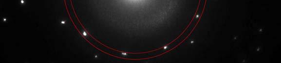
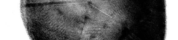
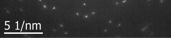
1 Supplementary Figure S1 X-ray diffraction pattern of the Ag nanowires shown in Fig. 1a dispersed in their original solution. The wavelength of the x-ray beam was Å. The saturated broad peak and the sloped background were due to the solvent and the quartz cuvette in which the dispersion of Ag nanowires was stored. As highlighted in the inset, the relative intensities between the (220) and (202)/(022) reflections are different from that shown in Fig. 1. The discrepancy is due to the high morphological anisotropy of the Ag nanowires. The longitudinal axis of each nanowire is along the [011] crystalline direction. When the dry Ag nanowires are deposited on a substrate, the orientations of all the {110} planes cannot be equally distributed due to the high aspect ratios of the nanowires. As a result, the relative diffraction intensities of the (220), (202), (022) reflections exhibit variations in comparison with the standard powder diffraction pattern. On the other hand, the Ag nanowires dispersed in a liquid solution randomly orient along different directions, leading to a diffraction pattern consistent with the standard pattern (red curve in Fig. 1d). S1
2 Supplementary Figure S2 X-ray diffraction patterns of Ag nanowires synthesized via different methods. (a) Fivefold multiply-twinned (MT) Ag nanowires with diameter of ~50 nm that were synthesized through the same method used for the nanowires shown in Fig. 1 except for a lower concentration of AgNO 3. (b) Fivefold MT Ag nanowires with diameter of ~110 nm that were synthesized through the same method used for the nanowires shown in Fig. 1 except that Fe(acac) 3 was replaced with Fe(NO 3 ) 3. (c) Fivefold MT Ag nanowires with diameter of ~60 nm that were synthesized through the reduction of AgNO 3 with glycerol in the absence of iron species [see the reference: Adv. Mater. 23, (2011)]. All the Ag nanowires exhibit the face-centered tetragonal (f.c.t.) phase. The splitting degree of the (200)/(020) and (002) reflections is dependent on the diameter of the nanowires and the synthetic methods. S2

 images of Ag")


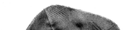
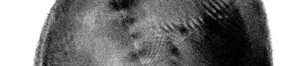
3 Supplementary Figure S3 Transmission electron microscopy (TEM) images of Ag nanocubes with an average size of 35 nm. The high-resolution TEM image in b clearly shows the single crystallinity of the nanocubes and defect-free lattice. According to the square symmetry of the lattice fringes, their surfaces can be determined to be bounded with {100} crystalline faces. S3
 Nanocubes with an average size of 35 nm as shown in Supplementary Figure S3. (b) Nanocubes with an average size of 120 nm. The wavelength of the x-ray beam was 0.")

4 Supplementary Figure S4 X-ray diffraction patterns of Ag nanocubes with different sizes. (a) Nanocubes with an average size of 35 nm as shown in Supplementary Figure S3. (b) Nanocubes with an average size of 120 nm. The wavelength of the x-ray beam was Å. The blue curves are the fitted results on the basis of the standard face-centered cubic (f.c.c.) phase with a correction of size-dependent broadening. The perfect matching between the fitting results and the measurement x-ray diffraction patterns indicates that defect-free Ag nanocubes are crystallized in f.c.c. phase regardless of their sizes. The peak indices correspond to the f.c.c phase of Ag. S4
, facecentered tetragonal (f.")

5 Supplementary Figure S5 Crystalline unit cells of face-centered cubic (f.c.c.), facecentered tetragonal (f.c.t.), and body-centered tetragonal (b.c.t.) phases and their relationship. S5
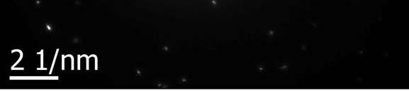
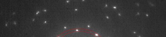
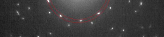
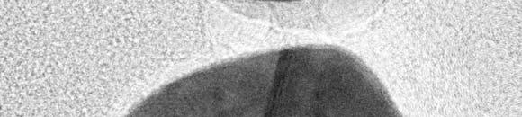
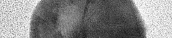
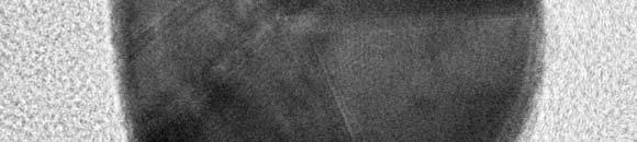
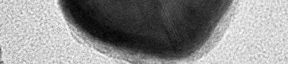
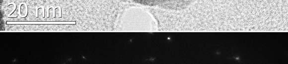
6 Supplementary Figure S6 Transmission electron microscopy (TEM) and electron diffraction (ED) characterization of Ag nanowires shown in Fig. 1a. (a) TEM image of randomly assembled Ag nanowires on a TEM grid. (b) ED pattern of a nanowire corresponding to the superposition of <110> (highlighted with yellow lines) and <111> (highlighted with red lines) zone axes. (c) ED pattern of a nanowire corresponding to the superposition of <100> (highlighted with green lines) and <112> (highlighted with blue lines) zone axes. S6

7 Supplementary Figure S7 Scanning electron microscopy image of the back side (i.e., the copper mesh side) of a transmission electron microscopy grid with Ag nanowires after the cross-sectional samples were prepared with the assistance of focused ion beam. The red arrows highlight the nanowires that were cut along the surfaces at 45 o with respect to the longitudinal axes of the nanowires. S7
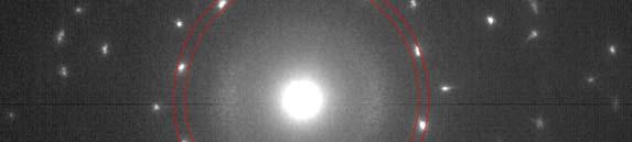
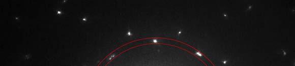
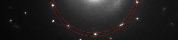
8 Supplementary Figure S8 Enlarged electron diffraction pattern of the one shown in Fig. 3e. All the (111) reflection spots between the two red circles exhibit clear splitting although the splitting levels for different spots are different. S8


9 Supplementary Figure S9 Transmission electron microscopy image and electron nanodiffraction patterns at different positions along the twin planes. The numbers represent the positions where the electron beam was located. The intensity profiles of the 222 reflection spots show their splitting degrees displayed in reciprocal space (nm 1 ). The difference between the two diffraction patterns along the same twin plane at different positions shows that the 222 reflect spot recorded from the core region exhibits larger splitting in comparison with the spot recorded from the surface region, indicating that the core of the nanowire has higher strain than its surface region. S9
10 Supplementary Figure S9 (continued) Comparison of electron diffraction patterns (left) and intensity profile of the 222 reflection spots along the straight lines shown in the electron diffraction patterns (right) at positions #1 and #2. S10
11 Supplementary Figure S9 (continued) Comparison of electron diffraction patterns (left) and intensity profile of the 222 reflection spots along the straight lines shown in the electron diffraction patterns (right) at positions #3 and #4. S11
12 Supplementary Figure S9 (continued) Comparison of electron diffraction patterns (left) and intensity profile of the 222 reflection spots along the straight lines shown in the electron diffraction patterns (right) at positions #5 and #6. The existence of more than 2 peaks in the intensity profile curve of position #6 indicates that there are more than two crystalline domains at position #6. S12
13 Supplementary Figure S9 (continued) Comparison of electron diffraction patterns (left) and intensity profile of the 222 reflection spots along the straight lines shown in the electron diffraction patterns (right) at positions #7 and #8. S13
14 Supplementary Figure S9 (continued) Comparison of electron diffraction patterns (left) and intensity profile of the 222 reflection spots along the straight lines shown in the electron diffraction patterns (right) at positions #9 and #10. S14

15 Supplementary Figure S10 Scanning electron microscopy images of the cross-sectional samples prepared by focused ion beam. S15
 image of crosssections of different nanowires shown")
 patterns.")


16 Supplementary Figure S11 Transmission electron microscopy (TEM) image of crosssections of different nanowires shown in Supplementary Figure S10 and their corresponding electron diffraction (ED) patterns. The cross sections shown in different images were made from different nanowires. The variation of the profiles of the cross sections is due to the difference between different nanowires. All the ED patterns show the splitting of the (111) reflection spots which are between the red circles. This figure corresponds to the wire #1 shown in Supplementary Figure S10. S16


17 Supplementary Figure S11 (continued) This figure corresponds to the wire #2 shown in Supplementary Figure S10. S17
18 Supplementary Figure S11 (continued) This figure corresponds to the wire #3 shown in Supplementary Figure S10. S18
19 Supplementary Figure S11 (continued) This figure corresponds to the wire #4 shown in Supplementary Figure S10. S19
 Scanning electron microscopy (SEM) image of the nanotubes.")

20 Supplementary Figure S12 Characterization of Ag-Au alloy nanotubes that were synthesized through the galvanic replacement reaction between the Ag nanowires shown in Fig. 1a and an aqueous solution of HAuCl 4 at 100 o C. (a) Scanning electron microscopy (SEM) image of the nanotubes. The open nanotubes clearly show the fivefold symmetry as same as that of the Ag nanowires. The small dots on the surfaces of the nanotubes correspond to AgCl nanoparticles and the Ag nanoparticles derived from the AgCl nanoparticles due to illumination of electron beam in SEM chamber. The inset in a is the schematic illustration to highlight the pentagonal cross section of the nanotubes and the existence of five twin planes in each nanotube. (b) Electron diffraction (ED) pattern of an individual nanotube obtained by aligning the electron beam perpendicular to one of the side surfaces of the nanotube as shown by the blue arrow in a. The ED pattern is essentially same as that obtained from a Ag nanowire as shown in Supplementary Figure S6c. The ED pattern corresponds to the superposition of <100> (highlighted with green lines) and <112> (highlighted with blue lines) zone axes. S20
21 solvent Intensity (counts) AgCl (111) AgCl (200) fcc (111) fcc (200) AgCl AgCl AgCl fcc (220) 4000 (200) (311) (222) θ ( o ) fct Ag (111) fct Ag (200) (020) fct Ag (002) fct Ag (220) fct Ag (202) (022) t (from 0 to 41 s) Supplementary Figure S13 Time-dependent x-ray diffraction patterns of the Ag nanowires during the replacement reaction. The strong background from the solvent was not subtracted. As the reaction proceeded, the face-centered tetragonal (f.c.t.) Ag nanowires were transformed to face-centered cubic (f.c.c.) Ag-Au alloy nanotubes and f.c.c AgCl solids were also formed due to the low solubility of AgCl. The wavelength of the x-ray beam was Å. S21
22 Supplementary Figure S14 Schematic drawing of a Ag nanowire with a highly strained core and a less strained (or unstrained) sheath. The core/shell structure expose strained lattices only at the ends of the nanowire to the surrounding environment. Due to the high reactivity of the strain surfaces and stability of the less strained side surfaces, the short nanowire formed at the early stage tend to grow longer by preferentially adding more Ag atoms to the strained surfaces. S22
Monitoring of Galvanic Replacement Reaction. between Silver Nanowires and HAuCl 4 by In-Situ. Transmission X-Ray Microscopy
 Supporting Information Monitoring of Galvanic Replacement Reaction between Silver Nanowires and HAuCl 4 by In-Situ Transmission X-Ray Microscopy Yugang Sun *, and Yuxin Wang Center for Nanoscale Materials
Supplementary Information
 Supplementary Information For Nearly Lattice Matched All Wurtzite CdSe/ZnTe Type II Core-Shell Nanowires with Epitaxial Interfaces for Photovoltaics Kai Wang, Satish C. Rai,Jason Marmon, Jiajun Chen, Kun
Supplementary information for: Surface passivated GaAsP single-nanowire solar cells exceeding 10% efficiency grown on silicon
 Supplementary information for: Surface passivated GaAsP single-nanowire solar cells exceeding 10% efficiency grown on silicon Jeppe V. Holm 1, Henrik I. Jørgensen 1, Peter Krogstrup 2, Jesper Nygård 2,4,
Multi-Functions of Net Surface Charge in the Reaction. on a Single Nanoparticle
 Multi-Functions of Net Surface Charge in the Reaction on a Single Nanoparticle Shaobo Xi 1 and Xiaochun Zhou* 1,2 1 Division of Advanced Nanomaterials, 2 Key Laboratory of Nanodevices and Applications,
SUPPLEMENTARY INFORMATION
 SUPPLEMENTARY INFORMATION doi:10.1038/nature11293 1. Formation of (111)B polar surface on Si(111) for selective-area growth of InGaAs nanowires on Si. Conventional III-V nanowires (NWs) tend to grow in
Synthesis of SiC nanowires from gaseous SiO and pyrolyzed bamboo slices
 Journal of Physics: Conference Series Synthesis of SiC nanowires from gaseous SiO and pyrolyzed bamboo slices To cite this article: Cui-yan Li et al 2009 J. Phys.: Conf. Ser. 152 012072 View the article
Integrated into Nanowire Waveguides
 Supporting Information Widely Tunable Distributed Bragg Reflectors Integrated into Nanowire Waveguides Anthony Fu, 1,3 Hanwei Gao, 1,3,4 Petar Petrov, 1, Peidong Yang 1,2,3* 1 Department of Chemistry,
Supplementary Information. Phase-selective cation-exchange chemistry in sulfide nanowire systems
 Supplementary Information Phase-selective cation-exchange chemistry in sulfide nanowire systems Dandan Zhang,, Andrew B. Wong,, Yi Yu,, Sarah Brittman,, Jianwei Sun,, Anthony Fu,, Brandon Beberwyck,,,
Low-energy Electron Diffractive Imaging for Three dimensional Light-element Materials
 Low-energy Electron Diffractive Imaging for Three dimensional Light-element Materials Hitachi Review Vol. 61 (2012), No. 6 269 Osamu Kamimura, Ph. D. Takashi Dobashi OVERVIEW: Hitachi has been developing
Raman Spectroscopy and Transmission Electron Microscopy of Si x Ge 1-x -Ge-Si Core-Double-Shell Nanowires
 Raman Spectroscopy and Transmission Electron Microscopy of Si x Ge 1-x -Ge-Si Core-Double-Shell Nanowires Paola Perez Mentor: Feng Wen PI: Emanuel Tutuc Background One-dimensional semiconducting nanowires
Observing Microorganisms through a Microscope LIGHT MICROSCOPY: This type of microscope uses visible light to observe specimens. Compound Light Micros
 PHARMACEUTICAL MICROBIOLOGY JIGAR SHAH INSTITUTE OF PHARMACY NIRMA UNIVERSITY Observing Microorganisms through a Microscope LIGHT MICROSCOPY: This type of microscope uses visible light to observe specimens.
Supplementary Figure 1. Effect of the spacer thickness on the resonance properties of the gold and silver metasurface layers.
 Supplementary Figure 1. Effect of the spacer thickness on the resonance properties of the gold and silver metasurface layers. Finite-difference time-domain calculations of the optical transmittance through
Supporting Information. Epitaxially Aligned Cuprous Oxide Nanowires for All-Oxide, Single-Wire Solar Cells
 Supporting Information Epitaxially Aligned Cuprous Oxide Nanowires for All-Oxide, Single-Wire Solar Cells Sarah Brittman, 1,2 Youngdong Yoo, 1 Neil P. Dasgupta, 1,3 Si-in Kim, 4 Bongsoo Kim, 4 and Peidong
Long-distance propagation of short-wavelength spin waves. Liu et al.
 Long-distance propagation of short-wavelength spin waves Liu et al. Supplementary Note 1. Characterization of the YIG thin film Supplementary fig. 1 shows the characterization of the 20-nm-thick YIG film
Nature Methods: doi: /nmeth Supplementary Figure 1. Resolution of lysozyme microcrystals collected by continuous rotation.
 Supplementary Figure 1 Resolution of lysozyme microcrystals collected by continuous rotation. Lysozyme microcrystals were visualized by cryo-em prior to data collection and a representative crystal is
Design, Fabrication, Characterization, and Application of Semiconductor Nanocomposites
 Design, Fabrication, Characterization, and Application of Semiconductor Nanocomposites Yang-Fang Chen Department of Physics, National Taiwan University, Taipei, Taiwan 1 I. A perfect integration of zero
Supplementary information for Stretchable photonic crystal cavity with
 Supplementary information for Stretchable photonic crystal cavity with wide frequency tunability Chun L. Yu, 1,, Hyunwoo Kim, 1, Nathalie de Leon, 1,2 Ian W. Frank, 3 Jacob T. Robinson, 1,! Murray McCutcheon,
Rapid, Low Temperature Synthesis of Germanium Nanowires from. Oligosilylgermane Precursors
 Supporting Information Rapid, Low Temperature Synthesis of Germanium Nanowires from Oligosilylgermane Precursors Mohammad Aghazadeh Meshgi a, Subhajit Biswas b,c, David McNulty b,, Colm O'Dwyer b, Giuseppe
Supplementary Information: Nanoscale. Structure, Dynamics, and Aging Behavior of. Metallic Glass Thin Films
 Supplementary Information: Nanoscale Structure, Dynamics, and Aging Behavior of Metallic Glass Thin Films J.A.J. Burgess,,, C.M.B. Holt,, E.J. Luber,, D.C. Fortin, G. Popowich, B. Zahiri,, P. Concepcion,
Supplementary Information
 Supplementary Information Supplementary Figure 1 Two blue-rayed limpets in their natural habitat on the stipe of a macroalgae. The surrounding light-yellow regions show exposed algal tissue eaten away
Supporting Information
 Supporting Information Ag nanowire synthesis All the chemicals were purchased from Sigma Aldrich and used without further purification. The synthesis of Ag nanowires was performed according to the polyol
High-Resolution Bubble Printing of Quantum Dots
 SUPPORTING INFORMATION High-Resolution Bubble Printing of Quantum Dots Bharath Bangalore Rajeeva 1, Linhan Lin 1, Evan P. Perillo 2, Xiaolei Peng 1, William W. Yu 3, Andrew K. Dunn 2, Yuebing Zheng 1,*
The 34th International Physics Olympiad
 The 34th International Physics Olympiad Taipei, Taiwan Experimental Competition Wednesday, August 6, 2003 Time Available : 5 hours Please Read This First: 1. Use only the pen provided. 2. Use only the
Electrochemical fabrication and magnetic properties of highly ordered silver nickel core-shell nanowires
 Journal of Alloys and Compounds 449 (2008) 232 236 Electrochemical fabrication and magnetic properties of highly ordered silver nickel core-shell nanowires Shih-Chin Lin a, San-Yuan Chen a,, Yun-Tien Chen
Optimization of supercontinuum generation in photonic crystal fibers for pulse compression
 Optimization of supercontinuum generation in photonic crystal fibers for pulse compression Noah Chang Herbert Winful,Ted Norris Center for Ultrafast Optical Science University of Michigan What is Photonic
SYNTHESIS AND CHARACTERIZATION OF II-IV GROUP AND SILICON RELATED NANOMATERIALS
 SYNTHESIS AND CHARACTERIZATION OF II-IV GROUP AND SILICON RELATED NANOMATERIALS ISMATHULLAKHAN SHAFIQ MASTER OF PHILOSOPHY CITY UNIVERSITY OF HONG KONG FEBRUARY 2008 CITY UNIVERSITY OF HONG KONG 香港城市大學
SUPPLEMENTARY INFORMATION
 SUPPLEMENTARY INFORMATION 1. Head-to-side welding mode In addition to aforementioned head-to-head and side-to-side joining geometries, cold-welding can also be realized in other geometries depending on
Supplementary Materials for
 www.sciencemag.org/cgi/content/full/science.1234855/dc1 Supplementary Materials for Taxel-Addressable Matrix of Vertical-Nanowire Piezotronic Transistors for Active/Adaptive Tactile Imaging Wenzhuo Wu,
FABRICATION AND CHARACTERIZATION OF NICKEL NANOWIRES
 FABRICATION AND CHARACTERIZATION OF NICKEL NANOWIRES Raminder Kaur Department of Basic and Applied Sciences, Punjabi University, Patiala, India ABSTRACT This paper shows that nickel nanowires of length
Supplemental information for Selective GaSb Radial Growth on Crystal Phase Engineered InAs Nanowires
 Electronic Supplementary Material (ESI) for Nanoscale. This journal is The Royal Society of Chemistry 2015 Supplemental information for Selective GaSb Radial Growth on Crystal Phase Engineered InAs Nanowires
SUPPLEMENTARY INFORMATION
 In the format provided by the authors and unedited. Photon-triggered nanowire transistors Jungkil Kim, Hoo-Cheol Lee, Kyoung-Ho Kim, Min-Soo Hwang, Jin-Sung Park, Jung Min Lee, Jae-Pil So, Jae-Hyuck Choi,
pattern. (c-e) TEM and HRTEM images of the nanowire (SAED pattern in inset).
 TEM and HRTEM images of the nanowire (SAED pattern in inset).") Figure S1. The pristine Co 2 (OH) 2 CO 3 nanowire arrays. (a) Low-magnification SEM image of the Co 2 (OH) 2 CO 3 nanowire arrays on nickel foam and (b) corresponding XRD pattern. (c-e) TEM and HRTEM images
Figure S1. The pristine Co 2 (OH) 2 CO 3 nanowire arrays. (a) Low-magnification SEM image of the Co 2 (OH) 2 CO 3 nanowire arrays on nickel foam and (b) corresponding XRD pattern. (c-e) TEM and HRTEM images
--> Buy True-PDF --> Auto-delivered in 0~10 minutes. JY/T
 Translated English of Chinese Standard: JY/T011-1996 www.chinesestandard.net Sales@ChineseStandard.net INDUSTRY STANDARD OF THE JY PEOPLE S REPUBLIC OF CHINA General rules for transmission electron microscopy
Supplementary Figure 1
 Supplementary Figure 1 Technical overview drawing of the Roadrunner goniometer. The goniometer consists of three main components: an inline sample-viewing microscope, a high-precision scanning unit for
Synthesis of Silver Nanowires with Reduced Diameters Using Benzoin-Derived Radicals to Make Transparent Conductors with High Transparency and Low Haze
 Supporting Information Synthesis of Silver Nanowires with Reduced Diameters Using Benzoin-Derived Radicals to Make Transparent Conductors with High Transparency and Low Haze Zhiqiang Niu,, Fan Cui,, Elisabeth
Project Staff: Timothy A. Savas, Michael E. Walsh, Thomas B. O'Reilly, Dr. Mark L. Schattenburg, and Professor Henry I. Smith
 9. Interference Lithography Sponsors: National Science Foundation, DMR-0210321; Dupont Agreement 12/10/99 Project Staff: Timothy A. Savas, Michael E. Walsh, Thomas B. O'Reilly, Dr. Mark L. Schattenburg,
Electronic Supplementary Information
 Electronic Supplementary Information Differential Interference Contrast Microscopy Imaging of Micrometer-Long Plasmonic Nanowires Ji Won Ha, Kuangcai Chen, and Ning Fang * Ames Laboratory, U.S. Department
Beam Shaping and Simultaneous Exposure by Diffractive Optical Element in Laser Plastic Welding
 Beam Shaping and Simultaneous Exposure by Diffractive Optical Element in Laser Plastic Welding AKL`12 9th May 2012 Dr. Daniel Vogler Page 1 Motivation: Quality and flexibility diffractive spot shaping
Supporting Information
 Supporting Information Eaton et al. 10.1073/pnas.1600789113 Additional Characterization and Simulation of CsPbX 3 Nanowires and Plates Atomic Force Microscopy Measurements. Atomic force microscopy (AFM)
The diffraction of light
 7 The diffraction of light 7.1 Introduction As introduced in Chapter 6, the reciprocal lattice is the basis upon which the geometry of X-ray and electron diffraction patterns can be most easily understood
SUPPORTING INFORMATION
 SUPPORTING INFORMATION Surface-Guided CsPbBr 3 Perovskite Nanowires on Flat and Faceted Sapphire with Size-Dependent Photoluminescence and Fast Photoconductive Response Eitan Oksenberg, Ella Sanders, Ronit
Supporting Information. for. Visualization of Electrode-Electrolyte Interfaces in LiPF 6 /EC/DEC Electrolyte for Lithium Ion Batteries via In-Situ TEM
 Supporting Information for Visualization of Electrode-Electrolyte Interfaces in LiPF 6 /EC/DEC Electrolyte for Lithium Ion Batteries via In-Situ TEM Zhiyuan Zeng 1, Wen-I Liang 1,2, Hong-Gang Liao, 1 Huolin
Hierarchical CoNiSe2 nano-architecture as a highperformance electrocatalyst for water splitting
 Nano Res. Electronic Supplementary Material Hierarchical CoNiSe2 nano-architecture as a highperformance electrocatalyst for water splitting Tao Chen and Yiwei Tan ( ) State Key Laboratory of Materials-Oriented
Supplementary Figure 1. GO thin film thickness characterization. The thickness of the prepared GO thin
 Supplementary Figure 1. GO thin film thickness characterization. The thickness of the prepared GO thin film is characterized by using an optical profiler (Bruker ContourGT InMotion). Inset: 3D optical
Fabrication of Probes for High Resolution Optical Microscopy
 Fabrication of Probes for High Resolution Optical Microscopy Physics 564 Applied Optics Professor Andrès La Rosa David Logan May 27, 2010 Abstract Near Field Scanning Optical Microscopy (NSOM) is a technique
Chapter 36: diffraction
 Chapter 36: diffraction Fresnel and Fraunhofer diffraction Diffraction from a single slit Intensity in the single slit pattern Multiple slits The Diffraction grating X-ray diffraction Circular apertures
*Corresponding author.
 Supporting Information for: Ligand-Free, Quantum-Confined Cs 2 SnI 6 Perovskite Nanocrystals Dmitriy S. Dolzhnikov, Chen Wang, Yadong Xu, Mercouri G. Kanatzidis, and Emily A. Weiss * Department of Chemistry,
SYNTHESIS AND ANALYSIS OF SILICON NANOWIRES GROWN ON Si (111) SUBSTRATE AT DIFFERENT SILANE GAS FLOW RATE
 SUBSTRATE AT DIFFERENT SILANE GAS FLOW RATE") SYNTHESIS AND ANALYSIS OF SILICON NANOWIRES GROWN ON Si (111) SUBSTRATE AT DIFFERENT SILANE GAS FLOW RATE Habib Hamidinezhad*, Yussof Wahab, Zulkafli Othaman and Imam Sumpono Ibnu Sina Institute for Fundamental
SYNTHESIS AND ANALYSIS OF SILICON NANOWIRES GROWN ON Si (111) SUBSTRATE AT DIFFERENT SILANE GAS FLOW RATE Habib Hamidinezhad*, Yussof Wahab, Zulkafli Othaman and Imam Sumpono Ibnu Sina Institute for Fundamental
Structural, optical, and electrical properties of phasecontrolled cesium lead iodide nanowires
 Electronic Supplementary Material Structural, optical, and electrical properties of phasecontrolled cesium lead iodide nanowires Minliang Lai 1, Qiao Kong 1, Connor G. Bischak 1, Yi Yu 1,2, Letian Dou
Growth and Characterization of single crystal InAs nanowire arrays and their application to plasmonics
 Growth and Characterization of single crystal InAs nanowire arrays and their application to plasmonics S.M. Prokes, H.D. Park* and O.J. Glembocki US Naval Research Laboratory 4555 Overlook Ave. SW, Washington
High-Speed Scalable Silicon-MoS 2 P-N Heterojunction Photodetectors
 High-Speed Scalable Silicon-MoS 2 P-N Heterojunction Photodetectors Veerendra Dhyani 1, and Samaresh Das 1* 1 Centre for Applied Research in Electronics, Indian Institute of Technology Delhi, New Delhi-110016,
Supplementary Materials for
 advances.sciencemag.org/cgi/content/full/3/10/eaao4204/dc1 Supplementary Materials for Enhanced mobility CsPbI3 quantum dot arrays for record-efficiency, high-voltage photovoltaic cells Erin M. Sanehira,
Supplementary Materials for
 advances.sciencemag.org/cgi/content/full/2/6/e1501326/dc1 Supplementary Materials for Organic core-sheath nanowire artificial synapses with femtojoule energy consumption Wentao Xu, Sung-Yong Min, Hyunsang
Chapter 28 Physical Optics: Interference and Diffraction
 Chapter 28 Physical Optics: Interference and Diffraction 1 Overview of Chapter 28 Superposition and Interference Young s Two-Slit Experiment Interference in Reflected Waves Diffraction Resolution Diffraction
Introduction to Transmission Electron Microscopy (Physical Sciences)
") Introduction to Transmission Electron Microscopy (Physical Sciences) Centre for Advanced Microscopy Program 9:30 10:45 Lecture 1 Basics of TEM 10:45 11:00 Morning tea 11:00 12:15 Lecture 2 Diffraction
Introduction to Transmission Electron Microscopy (Physical Sciences) Centre for Advanced Microscopy Program 9:30 10:45 Lecture 1 Basics of TEM 10:45 11:00 Morning tea 11:00 12:15 Lecture 2 Diffraction
Low-Temperature Solution-Phase Growth of Silicon and Silicon- Containing Alloy Nanowires
 Supporting Information for: Low-Temperature Solution-Phase Growth of Silicon and Silicon- Containing Alloy Nanowires Jianwei Sun 1,2,, Fan Cui 1,2,, Christian Kisielowski 3,4, Yi Yu 1, Nikolay Kornienko
Fabrication of a submicron patterned using an electrospun single fiber as mask. Author(s)Ishii, Yuya; Sakai, Heisuke; Murata,
Ishii, Yuya; Sakai, Heisuke; Murata,") JAIST Reposi https://dspace.j Title Fabrication of a submicron patterned using an electrospun single fiber as mask Author(s)Ishii, Yuya; Sakai, Heisuke; Murata, Citation Thin Solid Films, 518(2): 647-650
JAIST Reposi https://dspace.j Title Fabrication of a submicron patterned using an electrospun single fiber as mask Author(s)Ishii, Yuya; Sakai, Heisuke; Murata, Citation Thin Solid Films, 518(2): 647-650
High-resolution x-ray diffraction analysis of epitaxially grown indium phosphide nanowires
 JOURNAL OF APPLIED PHYSICS 97, 084318 2005 High-resolution x-ray diffraction analysis of epitaxially grown indium phosphide nanowires T. Kawamura, a S. Bhunia, b and Y. Watanabe c Basic Research Laboratories,
Supplementary Figure 1 High-resolution transmission electron micrograph of the
 Supplementary Figure 1 High-resolution transmission electron micrograph of the LAO/STO structure. LAO/STO interface indicated by the dotted line was atomically sharp and dislocation-free. Supplementary
Supporting Information
 Supporting Information Highly Stretchable and Transparent Supercapacitor by Ag-Au Core Shell Nanowire Network with High Electrochemical Stability Habeom Lee 1, Sukjoon Hong 2, Jinhwan Lee 1, Young Duk
NanoSpective, Inc Progress Drive Suite 137 Orlando, Florida
 TEM Techniques Summary The TEM is an analytical instrument in which a thin membrane (typically < 100nm) is placed in the path of an energetic and highly coherent beam of electrons. Typical operating voltages
Subcellular Neural Probes from Single Crystal. Gold Nanowires
 Supporting Information Subcellular Neural Probes from Single Crystal Gold Nanowires Mijeong Kang,, Seungmoon Jung, Huanan Zhang, Taejoon Kang, # Hosuk Kang, Youngdong Yoo, Jin-Pyo Hong, Jae-Pyoung Ahn,
Supplementary Figures
 Supplementary Figures Supplementary Figure 1 EM wave transport through a 150 bend. (a) Bend of our PEC-PMC waveguide. (b) Bend of the conventional PEC waveguide. Waves are incident from the lower left
Supplementary Information
 Supplementary Information Atomically flat single crystalline gold nanostructures for plasmonic nanocircuitry Jer Shing Huang 1,*, Victor Callegari 2, Peter Geisler 1, Christoph Brüning 1, Johannes Kern
7 CHAPTER 7: REFRACTIVE INDEX MEASUREMENTS WITH COMMON PATH PHASE SENSITIVE FDOCT SETUP
 7 CHAPTER 7: REFRACTIVE INDEX MEASUREMENTS WITH COMMON PATH PHASE SENSITIVE FDOCT SETUP Abstract: In this chapter we describe the use of a common path phase sensitive FDOCT set up. The phase measurements
Loss Compensation during Subwavelength Propagation of Enhanced Second Harmonic Generation in Hybrid Plasmonic Waveguide
 Electronic Supplementary Material (ESI) for Materials Chemistry Frontiers. This journal is the Partner Organisations 2018 Electronic Supplementary Information Loss Compensation during Subwavelength Propagation
Chapter Ray and Wave Optics
 109 Chapter Ray and Wave Optics 1. An astronomical telescope has a large aperture to [2002] reduce spherical aberration have high resolution increase span of observation have low dispersion. 2. If two
Photoconduction studies on GaN nanowire transistors under UV and polarized UV illumination
 Chemical Physics Letters 389 (24) 176 18 www.elsevier.com/locate/cplett Photoconduction studies on GaN nanowire transistors under UV and polarized UV illumination Song Han, Wu Jin, Daihua Zhang, Tao Tang,
Development of JEM-2800 High Throughput Electron Microscope
 Development of JEM-2800 High Throughput Electron Microscope Mitsuhide Matsushita, Shuji Kawai, Takeshi Iwama, Katsuhiro Tanaka, Toshiko Kuba and Noriaki Endo EM Business Unit, JEOL Ltd. Electron Optics
photolithographic techniques (1). Molybdenum electrodes (50 nm thick) are deposited by
. Molybdenum electrodes (50 nm thick) are deposited by") Supporting online material Materials and Methods Single-walled carbon nanotube (SWNT) devices are fabricated using standard photolithographic techniques (1). Molybdenum electrodes (50 nm thick) are deposited
Supporting online material Materials and Methods Single-walled carbon nanotube (SWNT) devices are fabricated using standard photolithographic techniques (1). Molybdenum electrodes (50 nm thick) are deposited
Solid-state physics. Bragg reflection: determining the lattice constants of monocrystals. LEYBOLD Physics Leaflets P
 Solid-state physics Properties of crystals X-ray structural analysis LEYBOLD Physics Leaflets Bragg reflection: determining the lattice constants of monocrystals P7.1.2.1 Objects of the experiment Investigating
write-nanocircuits Direct-write Jaebum Joo and Joseph M. Jacobson Molecular Machines, Media Lab Massachusetts Institute of Technology, Cambridge, MA
 Fab-in in-a-box: Direct-write write-nanocircuits Jaebum Joo and Joseph M. Jacobson Massachusetts Institute of Technology, Cambridge, MA April 17, 2008 Avogadro Scale Computing / 1 Avogadro number s? Intel
High-Quality Metal Oxide Core/Shell Nanowire Arrays on Conductive Substrates for Electrochemical Energy Storage. and Hong Jin Fan, *
 Supporting Information for High-Quality Metal Oxide Core/Shell Nanowire Arrays on Conductive Substrates for Electrochemical Energy Storage Xinhui Xia, Jiangping Tu,, * Yongqi Zhang, Xiuli Wang, Changdong
Supplementary Figure S1. Schematic representation of different functionalities that could be
 Supplementary Figure S1. Schematic representation of different functionalities that could be obtained using the fiber-bundle approach This schematic representation shows some example of the possible functions
Magnesium and Magnesium-Silicide coated Silicon Nanowire composite Anodes for. Lithium-ion Batteries
 Magnesium and Magnesium-Silicide coated Silicon Nanowire composite Anodes for Lithium-ion Batteries Alireza Kohandehghan a,b, Peter Kalisvaart a,b,*, Martin Kupsta b, Beniamin Zahiri a,b, Babak Shalchi
Supplementary Information for: Immersion Meta-lenses at Visible Wavelengths for Nanoscale Imaging
 Supplementary Information for: Immersion Meta-lenses at Visible Wavelengths for Nanoscale Imaging Wei Ting Chen 1,, Alexander Y. Zhu 1,, Mohammadreza Khorasaninejad 1, Zhujun Shi 2, Vyshakh Sanjeev 1,3
Deliverable 4.2: TEM cross sections on prototyped Gated Resistors
 Deliverable 4.2: TEM cross sections on prototyped Gated Resistors Olga G. Varona, Geoff Walsh, Bernie Capraro Intel Ireland 21 June 2011 Abbreviation list D: drain FIB: focused ion-beam HRTEM: high resolution
SUPPLEMENTARY INFORMATION Polarization response of nanowires à la carte
 * Correspondence to anna.fontcuberta-morral@epfl.ch SUPPLEMENTARY INFORMATION Polarization response of nanowires à la carte Alberto Casadei, Esther Alarcon Llado, Francesca Amaduzzi, Eleonora Russo-Averchi,
Supporting Information: Achromatic Metalens over 60 nm Bandwidth in the Visible and Metalens with Reverse Chromatic Dispersion
 Supporting Information: Achromatic Metalens over 60 nm Bandwidth in the Visible and Metalens with Reverse Chromatic Dispersion M. Khorasaninejad 1*, Z. Shi 2*, A. Y. Zhu 1, W. T. Chen 1, V. Sanjeev 1,3,
Circular Dichroism Microscopy Free from Commingling Linear Dichroism via Discretely Modulated Circular Polarization
 Supplementary information Circular Dichroism Microscopy Free from Commingling Linear Dichroism via Discretely Modulated Circular Polarization Tetsuya Narushima AB and Hiromi Okamoto A* A Institute for
Introduction to Electron Microscopy
 Introduction to Electron Microscopy Prof. David Muller, dm24@cornell.edu Rm 274 Clark Hall, 255-4065 Ernst Ruska and Max Knoll built the first electron microscope in 1931 (Nobel Prize to Ruska in 1986)
plasmonic nanoblock pair
 Nanostructured potential of optical trapping using a plasmonic nanoblock pair Yoshito Tanaka, Shogo Kaneda and Keiji Sasaki* Research Institute for Electronic Science, Hokkaido University, Sapporo 1-2,
Transmission electron Microscopy
 Transmission electron Microscopy Image formation of a concave lens in geometrical optics Some basic features of the transmission electron microscope (TEM) can be understood from by analogy with the operation
SUPPLEMENTARY INFORMATION
 Enhanced Thermoelectric Performance of Rough Silicon Nanowires Allon I. Hochbaum 1 *, Renkun Chen 2 *, Raul Diaz Delgado 1, Wenjie Liang 1, Erik C. Garnett 1, Mark Najarian 3, Arun Majumdar 2,3,4, Peidong
Name. Light Chapter Summary Cont d. Refraction
 Page 1 of 17 Physics Week 12(Sem. 2) Name Light Chapter Summary Cont d with a smaller index of refraction to a material with a larger index of refraction, the light refracts towards the normal line. Also,
Chapter 4 Imaging Lecture 17
 Chapter 4 Imaging Lecture 17 d (110) Imaging Imaging in the TEM Diffraction Contrast in TEM Image HRTEM (High Resolution Transmission Electron Microscopy) Imaging STEM imaging Imaging in the TEM What is
X-ray investigation of crystal structures / Laue method with digital X-ray detector (XRIS) (Item No.: P )
 (Item No.: P )") X-ray investigation of crystal structures / Laue method with digital X-ray detector (XRIS) (Item No.: P2541602) Curricular Relevance Area of Expertise: Physik Education Level: Hochschule Topic: Moderne
X-ray investigation of crystal structures / Laue method with digital X-ray detector (XRIS) (Item No.: P2541602) Curricular Relevance Area of Expertise: Physik Education Level: Hochschule Topic: Moderne
Vertical Nanowall Array Covered Silicon Solar Cells
 International Conference on Solid-State and Integrated Circuit (ICSIC ) IPCSIT vol. () () IACSIT Press, Singapore Vertical Nanowall Array Covered Silicon Solar Cells J. Wang, N. Singh, G. Q. Lo, and D.
MSE 595T Transmission Electron Microscopy. Laboratory III TEM Imaging - I
 MSE 595T Basic Transmission Electron Microscopy TEM Imaging - I Purpose The purpose of this lab is to: 1. Make fine adjustments to the microscope alignment 2. Obtain a diffraction pattern 3. Obtain an
Supporting Information. Single-Nanowire Electrochemical Probe Detection for Internally Optimized Mechanism of
 Supporting Information Single-Nanowire Electrochemical Probe Detection for Internally Optimized Mechanism of Porous Graphene in Electrochemical Devices Ping Hu, Mengyu Yan, Xuanpeng Wang, Chunhua Han,*
A novel tunable diode laser using volume holographic gratings
 A novel tunable diode laser using volume holographic gratings Christophe Moser *, Lawrence Ho and Frank Havermeyer Ondax, Inc. 85 E. Duarte Road, Monrovia, CA 9116, USA ABSTRACT We have developed a self-aligned
Supplementary Information
 Electronic Supplementary Material (ESI) for Physical Chemistry Chemical Physics. This journal is the Owner Societies 2014 Supplementary Information Single-crystalline CdTe nanowire field effect transisitor
Transparent p-type SnO Nanowires with Unprecedented Hole Mobility among Oxide Semiconductors
 Supplementary Information Transparent p-type SnO Nanowires with Unprecedented Hole Mobility among Oxide Semiconductors J. A. Caraveo-Frescas and H. N. Alshareef* Materials Science and Engineering, King
Final Report for AFOSR Project
 Final Report for AFOSR Project March 19, 2007 Title Synthesis and modulation of visible-bandgap semiconductor nanowires and their optical sensor application Research Period: 2006. 1. 1 ~ 2006. 12. 31 Principal
OPTICAL SYSTEMS OBJECTIVES
 101 L7 OPTICAL SYSTEMS OBJECTIVES Aims Your aim here should be to acquire a working knowledge of the basic components of optical systems and understand their purpose, function and limitations in terms
2.1 BASIC THEORY: INTERFERENCE OF TWO BEAMS
 2 LASER INTERFERENCE LITHOGRAPHY (LIL) 9 2 LASER INTERFERENCE LITHOGRAPHY (LIL) Laser interference lithography [3~22] (LIL) is a method to produce periodic structures using two interfering highly-coherent
Electronic Supplementary Information:
 Electronic Supplementary Material (ESI) for Journal of Materials Chemistry A. This journal is The Royal Society of Chemistry 2017 Electronic Supplementary Information: Fabrication and optical characterization
Switchable reflective lens based on cholesteric liquid crystal
 Switchable reflective lens based on cholesteric liquid crystal Jae-Ho Lee, 1,3 Ji-Ho Beak, 2,3 Youngsik Kim, 2 You-Jin Lee, 1 Jae-Hoon Kim, 1,2 and Chang-Jae Yu 1,2,* 1 Department of Electronic Engineering,
GEOMETRICAL OPTICS Practical 1. Part I. BASIC ELEMENTS AND METHODS FOR CHARACTERIZATION OF OPTICAL SYSTEMS
 GEOMETRICAL OPTICS Practical 1. Part I. BASIC ELEMENTS AND METHODS FOR CHARACTERIZATION OF OPTICAL SYSTEMS Equipment and accessories: an optical bench with a scale, an incandescent lamp, matte, a set of
Bruker D8 HRXRD. Collecting Reciprocal Space Maps using the LynxEye Position Sensitive Detector
 Bruker D8 HRXRD Collecting Reciprocal Space Maps using the LynxEye Position Sensitive Detector Scott A Speakman, Ph.D. MIT Center for Materials Science and Engineering For help in the X-ray Lab, contact