Basic Principles, Challenges and Opportunities of STT-MRAM for Embedded Memory Applications
|
|
|
- Philomena Lindsey
- 6 years ago
- Views:
Transcription

1 Basic Principles, Challenges and Opportunities of STT-MRAM for Embedded Memory Applications Luc Thomas TDK- Headway Technologies, 463 S. Milpitas Boulevard, Milpitas CA 95035, USA

2 MRAM Team at TDK - Headway Tech. Guenole Jan, Son Le, Santiago Serrano-Guisan Yuan-Jen Lee, Huanlong Liu, Jian Zhu, Jodi Iwata-Harms, Ru-Ying Tong, Sahil Patel, Vignesh Sundar, Dongna Shen, Yi Yang, Renren He, Jesmin Haq, Jeffrey Teng, Vinh Lam, Paul Liu, Yu-Jen Wang, Tom Zhong, and Po-Kang Wang.


")
3 Magnetic Random Access Memories More than 20 years ago: Field-MRAM 1 st research program: IBM / Motorola (1995) 1 st product: Freescale / Everspin (2006) From S. Parkin and K. Roche IBM


4 60 years ago: TDK first foray in MRAM technology TDK s 18x24 bit Magnetic Core Memory Source: columbia.edu/cu/computinghistory/core.html Source: wikipedia.org/wiki/magnetic-core_memory MRAM was the predominant computer memory from the 50 s to the 70 s
5 Outline Basic principles of STT-MRAM STT-MRAM integration STT-MRAM in emerging memory landscape

6 Magnetic Tunnel Junction (MTJ) device Two ferromagnetic electrodes separated by a thin MgO tunnel barrier Tunnel Magnetoresistance (TMR): device resistance depends on the relative orientation of the magnetization of the two magnetic electrodes From S. Parkin and K. Roche IBM Yuasa et al. (AIST) Nature Materials2004
7 Magnetic Tunnel Junction (MTJ) device Two ferromagnetic electrodes separated by a thin MgO tunnel barrier Tunnel Magnetoresistance (TMR): device resistance depends on the relative orientation of the magnetization of the two magnetic electrodes Reproduced from website of MultiDimension Technology Co.,Ltd. Yuasa et al. (AIST) Nature Materials2004

 Free layer sandwiched between to MgO interfaces for the free layer")

8 Perpendicular Magnetic Anisotropy (PMA) MTJ PMA is needed for data retention scaling and writing efficiency PMA is based on interfacial anisotropy between MgO and CoFeB Ikeda et al., Nature Mat. 2011, Worledge et al., APL 2012) Free layer sandwiched between to MgO interfaces for the free layer for enhanced anisotropy and data retention Dual reference layer for reducing dipolar fields and enhanced stability Free Layer Pinned Layer 1 Ikeda et al., IEDM2014 Pinned Layer 2
9 High data retention in PMA-MTJs Developed a MTJ stack of high PMA and thermal stability to satisfy solder reflow requirement of 260ºC for 90 seconds (2016 VLSI TSMC/TDK) Method of projecting error rate from chip level data in ppm regime 1ppm 10 years retention at 225ºC
10 Resistance vs magnetic field hysteresis loops AP state 9000 R (Ohms) P state Magnetic field H (koe) Two well-defined resistance states depending on orientation of magnetic electrodes


11 Reading with Tunnel Magnetoresistance Read operation by probing the resistance of the device at low voltage bias True Binary device: no resistance drift of the 2 resistance state even after repeated cycling at maximum drive current Resistance High R state 1 Low R state 0 After endurance test 100k devices Current Before endurance test


 Write: Spin")
12 Writing with Spin-Transfer Torque Transfer of spin-angular momentum from polarized conduction electrons to electrodes magnetization Resistance 2 Read: Tunnel Magnetoresistance 1 1 Reproduced from Quantumwise.com Phenomenon discovered in 1996 by two theoreticians: John Slonczewski (IBM) Luc Berger (Carnegie Mellon) Write: Spin Transfer Torque Voltage 2 4 electron flow electron flow
 - smaller device -> smaller current requirement Current")
 1 0-1 Write 1 Write 0 10ns 10us 10ms Pulse Length")
13 Trade-offs of STT writing Switching Current scales with area (constant current density) - smaller device -> smaller current requirement Current inversely proportional to pulse width - faster -> higher current requirement Normalized Voltage (a.u.) Write 1 Write 0 10ns 10us 10ms Pulse Length

14 Trade-offs of STT writing (cont d) Write current scales with energy barrier for data retention Energy barrier: E B ~ K u V Write current: I c0 = (4e/ħ) (α/p) E B STT efficiency: E B /I c0 ~ 1-2 in k B T/µA Writing is probabilistic STT vanishes for parallel alignment of PL and FL Switching time inversely proportional to angle between PL and FL Thermal fluctuations provide initial kick PMA_Ms1200_K=1e7_60x60x2_c2_a=0v01_Pz=pos10d_I=500uA Mx(ave) My(ave) Mz(ave) Mx(ave) Time(ps)
15 Outline Basic principles of STT-MRAM STT-MRAM integration STT-MRAM in emerging memory landscape
 1T-1MTJ IBM s")


16 Integration of 8 Mb test chips at TDK - Headway 8Mbits (16x512k) 1T-1MTJ IBM s 90nm CMOS technology 50F 2 cell size Sense Amplifiers for reading Redundancy and 2bit ECC FEOL in IBM foundry BEOL in TDK-Headway s fab BLT WL Access Transistor BLC
 to standard")

17 STT MRAM process integration MRAM only add three additional layers (MTJ and electrodes) to standard CMOS BEOL: 3 to 4 mask adder MTJ stack is about 20 nm thick, can be easily integrated into CMOS backend process
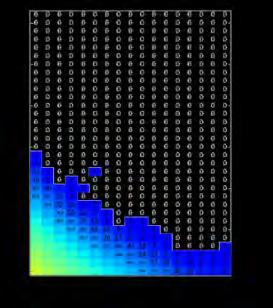
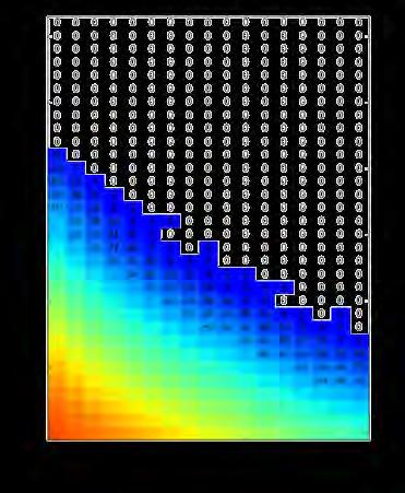
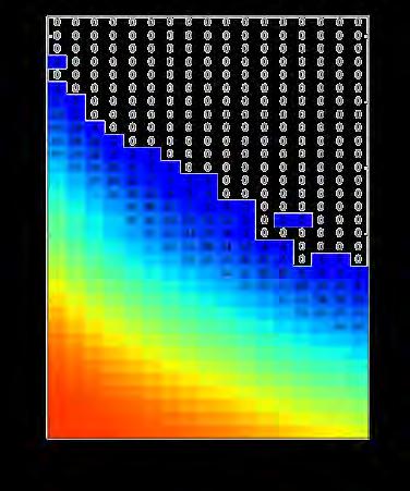
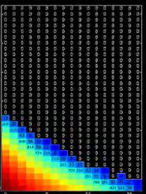
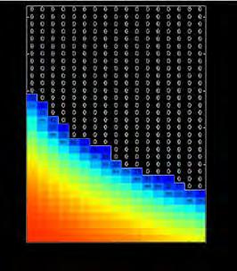
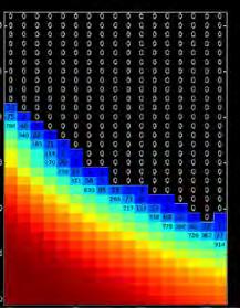
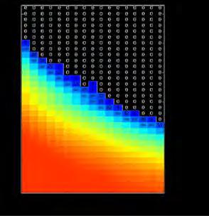
18 Defect rate of 8 Mb chip Distribution of device current in the P state Quantile plot Log scale 1 ppm read current (a.u.) read current (a.u.) less than 0.4 ppm defect rate
19 400C annealing after MTJ patterning 400C BEOL process can add up to several hours, depending on how many metal layers on top of MTJ Elemental movements and morphology changes can degrade anisotropy, exchange coupling, and defect level - selection of materials, diffusion barrier and interface/growth quality - Thorough engineering needed for electrodes, film stack, process, encapsulation 2.5 after MTJ etching Diameter ~ 30 nm (electrical) DRR = 175% RA of 8.5 Ω-µm 2 H C = 3300 Oe with no offset
20 Error free writing in chip level (TDK VLSI2014 & 2016) Error free writing on 8 Mb chips without ECC Down to 6 ns write pulse While keep data retention to 142ºC for 10 years 142ºC for 10 years eff Temperature (ºC)
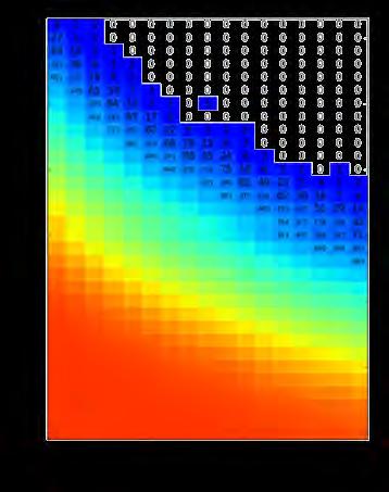
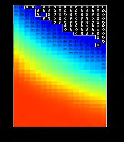
21 Temperature dependence (TDK VLSI2014) Fast operation down to 4.5 ns demonstrated over wide temperature range -25 C 0 C 25 C 55 C 85 C 125 C No ECC No Error bit ECC
22 Outline Basic principles of STT-MRAM STT-MRAM integration STT-MRAM in emerging memory landscape

23 STT-MRAM vs other memory technologies


24 STT-MRAM requirements Critical requirements depend on application from S.H Kang, Qualcomm (Proc. VLSI 2014)
25 STT-MRAM Challenge Cost is directly related to density & cell/chip size Current available scales with transistor size - Standalone DRAM : GB chips, cell size ~4F 2 F smallest feature at technology node (28,20,14/16nm, ) MTJ < 20 nm Write current < 20 µa TMR ~ 300% - Embedded Flash / DRAM : cell size ~40-50F 2 MTJ ~ nm Write current > 100 µa TMR > 100% Kent & Worledge, Nature Nano (2015)
 Almost universal memory Combines")
26 Embedded STT-MRAM is cheaper and better! Lower cost Similar or Smaller bit cell size Very few added mask layers Does not interfere with CMOS transistor performances (as a add-on in the backend metal layers) Almost universal memory Combines non-volatility, high speed, and infinite endurance Can replace eflash, edram, and last-level cache (LLC) SRAM Efficient system architectures, without moving data between code storage, and working memory, and data storage Higher energy efficiency (longer battery life) mobile and IoT applications have low duty cycles and need fast wake-up and low standby power

27 6-Transistor SRAM scaling challenge 22nm to 10 nm node: - Expected area scaling: 4.8X - Actual scaling: ~ 2X 400F 2 at 10nm vs 52F 2 at 40nm Samsung VLSI 2016 Complex design limits scaling Dramatic increase of the area occupied by memory vs logic in performance SoC and CPU s


 2.3ns 1.8ns 1.")
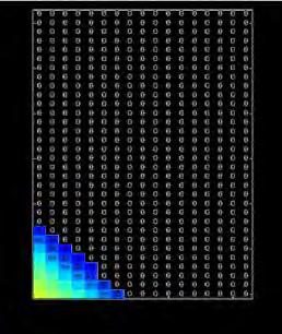
28 Opportunity for emram as Last Level Cache Compact design 1T-1MTJ 8 Mb written without error with 1.5 ns write pulse NO ECC Voltage (a.u) 2.3ns 1.8ns 1.5ns TDK VLSI / Pulse width
29 Summary STT-MRAM combine low write current, data retention and write speed, and is compatible with BEOL processes. Working chips have been demonstrated MTJ device can be tailored to specific applications that require data retention or speed, Great opportunity for embedded applications from eflash to SRAM replacement (both Samsung and TSMC have announced production) Many challenges remain: writing efficiency, read margin (TMR), process control (tight pitch, uniformity),

30 1970: Magnetic memories lose the war to Silicon 2017: year of the comeback for MRAM? Circa 1970 Intel corporation - Computer history museum
Status and Prospect for MRAM Technology
 Status and Prospect for MRAM Technology Dr. Saied Tehrani Nonvolatile Memory Seminar Hot Chips Conference August 22, 2010 Memorial Auditorium Stanford University Everspin Technologies, Inc. - 2010 Agenda
A novel sensing algorithm for Spin-Transfer-Torque magnetic RAM (STT-MRAM) by utilizing dynamic reference
 by utilizing dynamic reference") A novel sensing algorithm for Spin-Transfer-Torque magnetic RAM (STT-MRAM) by utilizing dynamic reference Yong-Sik Park, Gyu-Hyun Kil, and Yun-Heub Song a) Department of Electronics and Computer Engineering,
A novel sensing algorithm for Spin-Transfer-Torque magnetic RAM (STT-MRAM) by utilizing dynamic reference Yong-Sik Park, Gyu-Hyun Kil, and Yun-Heub Song a) Department of Electronics and Computer Engineering,
Magnetic Spin Devices: 7 Years From Lab To Product. Jim Daughton, NVE Corporation. Symposium X, MRS 2004 Fall Meeting
 Magnetic Spin Devices: 7 Years From Lab To Product Jim Daughton, NVE Corporation Symposium X, MRS 2004 Fall Meeting Boston, MA December 1, 2004 Outline of Presentation Early Discoveries - 1988 to 1995
An 8-bit Analog-to-Digital Converter based on the Voltage-Dependent Switching Probability of a Magnetic Tunnel Junction
 An 8-bit Analog-to-Digital Converter based on the Voltage-Dependent Switching Probability of a Magnetic Tunnel Junction Won Ho Choi*, Yang Lv*, Hoonki Kim, Jian-Ping Wang, and Chris H. Kim *equal contribution
Lecture #29. Moore s Law
 Lecture #29 ANNOUNCEMENTS HW#15 will be for extra credit Quiz #6 (Thursday 5/8) will include MOSFET C-V No late Projects will be accepted after Thursday 5/8 The last Coffee Hour will be held this Thursday
A REVIEW ON MAGNETIC TUNNEL JUNCTION TECHNOLOGY
 A REVIEW ON MAGNETIC TUNNEL JUNCTION TECHNOLOGY Pawan Choudhary 1, Dr. Kanika Sharma 2, Sagar Balecha 3, Bhaskar Mishra 4 1 M.E Scholar, Electronics & Communication Engineering, National Institute of Technical
MAGNETORESISTIVE random access memory
 132 IEEE TRANSACTIONS ON MAGNETICS, VOL. 41, NO. 1, JANUARY 2005 A 4-Mb Toggle MRAM Based on a Novel Bit and Switching Method B. N. Engel, J. Åkerman, B. Butcher, R. W. Dave, M. DeHerrera, M. Durlam, G.
S1. Current-induced switching in the magnetic tunnel junction.
 S1. Current-induced switching in the magnetic tunnel junction. Current-induced switching was observed at room temperature at various external fields. The sample is prepared on the same chip as that used
Quantitative evaluation of reliability and performance for STT-MRAM
 Quantitative evaluation of reliability and performance for STT-MRAM Liuyang Zhang, Aida Todri-Sanial, Wang Kang, Youguang Zhang, Lionel Torres, Yuanqing Cheng, Weisheng Zhao To cite this version: Liuyang
IBM Research Report. Research Division Almaden - Austin - Beijing - Cambridge - Haifa - India - T. J. Watson - Tokyo - Zurich
 RC24655 (W0809-114) September 29, 2008 Physics IBM Research Report Field and Bias Dependence of High-frequency Magnetic Noise in MgO-based Magnetic Tunnel Junctions Y. Guan, D. W. Abraham, M. C. Gaidis,
SUPPLEMENTARY INFORMATION
 Induction of coherent magnetization switching in a few atomic layers of FeCo using voltage pulses Yoichi Shiota 1, Takayuki Nozaki 1, 2,, Frédéric Bonell 1, Shinichi Murakami 1,2, Teruya Shinjo 1, and
VARIATION MONITOR-ASSISTED ADAPTIVE MRAM WRITE
 Shaodi Wang, Hochul Lee, Pedram Khalili, Cecile Grezes, Kang L. Wang and Puneet Gupta University of California, Los Angeles VARIATION MONITOR-ASSISTED ADAPTIVE MRAM WRITE NanoCAD Lab shaodiwang@g.ucla.edu
Highly Reliable Memory-based Physical Unclonable Function Using Spin-Transfer Torque MRAM
 Highly Reliable Memory-based Physical Unclonable Function Using Spin-Transfer Torque MRAM Le Zhang 1, Xuanyao Fong 2, Chip-Hong Chang 1, Zhi Hui Kong 1, Kaushik Roy 2 1 School of EEE, Nanyang Technological
STT-MRAM Read-circuit with Improved Offset Cancellation
 JOURNAL OF SEMICONDUCTOR TECHNOLOGY AND SCIENCE, VOL.17, NO.3, JUNE, 2017 ISSN(Print) 1598-1657 https://doi.org/10.5573/jsts.2017.17.3.347 ISSN(Online) 2233-4866 STT-MRAM Read-circuit with Improved Offset
MTJ Variation Monitor-assisted Adaptive MRAM Write
 MTJ Variation Monitor-assisted Adaptive MRAM Write Shaodi Wang shaodiwang@g.ucla.edu Pedram Khalili pedramk@ucla.edu Hochul Lee chul0524@ucla.edu Kang L. Wang wang@ee.ucla.edu Cecile Grezes grezes.cecile@gmail.com
Mayank Chakraverty and Harish M Kittur. VIT University, Vellore, India,
 International Journal of Micro and Nano Systems, 2(1), 2011, pp. 1-6 FIRST PRINCIPLE SIMULATIONS OF FE/MGO/FE MAGNETIC TUNNEL JUNCTIONS FOR APPLICATIONS IN MAGNETORESISTIVE RANDOM ACCESS MEMORY BASED CELL
Semiconductor Memory: DRAM and SRAM. Department of Electrical and Computer Engineering, National University of Singapore
 Semiconductor Memory: DRAM and SRAM Outline Introduction Random Access Memory (RAM) DRAM SRAM Non-volatile memory UV EPROM EEPROM Flash memory SONOS memory QD memory Introduction Slow memories Magnetic
Magnetic tunnel junction sensor development for industrial applications
 Magnetic tunnel junction sensor development for industrial applications Introduction Magnetic tunnel junctions (MTJs) are a new class of thin film device which was first successfully fabricated in the
Tunneling Magnetoresistance Devices with MgO barrier and CoFeB electrodes for Magnetic. Field
 Tunneling Magnetoresistance Devices with MgO barrier and CoFeB electrodes for Magnetic Field Sensors Piotr Wiśniowski Michał Dąbek Department of Electronics AGH-University of Science and Technology NANOSPIN-Meeting,
Application Note Model 765 Pulse Generator for Semiconductor Applications
 Application Note Model 765 Pulse Generator for Semiconductor Applications Non-Volatile Memory Cells Characterization The trend of memory research is to develop a new memory called Non-Volatile RAM that
In pursuit of high-density storage class memory
 Edition October 2017 Semiconductor technology & processing In pursuit of high-density storage class memory A novel thermally stable GeSe-based selector paves the way to storage class memory applications.
A Spin-Torque Transfer MRAM in 90nm CMOS. Hui William Song
 A Spin-Torque Transfer MRAM in 90nm CMOS by Hui William Song A thesis submitted in conformity with the requirements for the degree of Master of Applied Science Graduate Department of Electrical and Computer
40nm Node CMOS Platform UX8
 FUKAI Toshinori, IKEDA Masahiro, TAKAHASHI Toshifumi, NATSUME Hidetaka Abstract The UX8 is the latest process from NEC Electronics. It uses the most advanced exposure technology to achieve twice the gate
A Low-Power Robust Easily Cascaded PentaMTJ-Based Combinational and Sequential Circuits Mohit Kumar Gupta and Mohd Hasan, Senior Member, IEEE
 IEEE TRANSACTIONS ON VERY LARGE SCALE INTEGRATION (VLSI) SYSTEMS 1 A Low-Power Robust Easily Cascaded PentaMTJ-Based Combinational and Sequential Circuits Mohit Kumar Gupta and Mohd Hasan, Senior Member,
A Scaling Roadmap and Performance Evaluation of In-Plane and Perpendicular MTJ Based STT-MRAMs for High-Density Cache Memory
 598 IEEE JOURNAL OF SOLID-STATE CIRCUITS, VOL. 48, NO. 2, FEBRUARY 2013 A Scaling Roadmap and Performance Evaluation of In-Plane and Perpendicular MTJ Based STT-MRAMs for High-Density Cache Memory Ki Chul
COMMERCIAL APPLICATIONS OF SPINTRONICS TECHNOLOGY
 Presented at Nanomaterials 2004, Stamford, CT, October 25, 2004 COMMERCIAL APPLICATIONS OF SPINTRONICS TECHNOLOGY Carl H. Smith Senior Physicist, Advanced Technology Group NVE Corporation 11409 Valley
Breaking Through Impenetrable Barriers
 Breaking Through Impenetrable Barriers The Key to the Evolution of Solid State Memory A Pictorial Approach Andrew J. Walker PhD August 2018 1 The Link between α-particles, 3-D NAND and MRAM? - Quantum
HfO 2 Based Resistive Switching Non-Volatile Memory (RRAM) and Its Potential for Embedded Applications
 and Its Potential for Embedded Applications") 2012 International Conference on Solid-State and Integrated Circuit (ICSIC 2012) IPCSIT vol. 32 (2012) (2012) IACSIT Press, Singapore HfO 2 Based Resistive Switching Non-Volatile Memory (RRAM) and Its
2012 International Conference on Solid-State and Integrated Circuit (ICSIC 2012) IPCSIT vol. 32 (2012) (2012) IACSIT Press, Singapore HfO 2 Based Resistive Switching Non-Volatile Memory (RRAM) and Its
64 Kb logic RRAM chip resisting physical and side-channel attacks for encryption keys storage
 64 Kb logic RRAM chip resisting physical and side-channel attacks for encryption keys storage Yufeng Xie a), Wenxiang Jian, Xiaoyong Xue, Gang Jin, and Yinyin Lin b) ASIC&System State Key Lab, Dept. of
Variation-tolerant Non-volatile Ternary Content Addressable Memory with Magnetic Tunnel Junction
 JOURNAL OF SEMICONDUCTOR TECHNOLOGY AND SCIENCE, VOL.17, NO.3, JUNE, 2017 ISSN(Print) 1598-1657 https://doi.org/10.5573/jsts.2017.17.3.458 ISSN(Online) 2233-4866 Variation-tolerant Non-volatile Ternary
Sensing Circuits for Resistive Memory
 Sensing Circuits for Resistive Memory R. Jacob, Ph.D., P.E. Department of Electrical Engineering Boise State University 1910 University Dr., ET 201 Boise, ID 83725 jbaker@ieee.org Abstract A nascent class
MgO MTJ biosensors for immunomagnetic lateralflow
 MgO MTJ biosensors for immunomagnetic lateralflow detection Ricardo Jorge Penelas Janeiro Under supervision of Susana Isabel Pinheiro Cardoso de Freitas Dep. Physics, IST, Lisbon, Portugal Octrober 15,
Energy-efficient neuromorphic computing with magnetic tunnel junctions
 Energy-efficient neuromorphic computing with magnetic tunnel junctions CNRS/Thales, France Jacob Torrejon Mathieu Riou Flavio Abreu Araujo Paolo Bortolotti Vincent Cros Julie Grollier AIST, Japan Sumito
US A1 (19) United States (12) Patent Application Publication (10) Pub. N0.: US 2013/ A1 Zhou et a]. (43) Pub. Date: Aug.
![US A1 (19) United States (12) Patent Application Publication (10) Pub. N0.: US 2013/ A1 Zhou et a]. (43) Pub. Date: Aug.](/thumbs/83/87424156.jpg "US A1 (19) United States (12) Patent Application Publication (10) Pub. N0.: US 2013/ A1 Zhou et a]. (43) Pub. Date: Aug.") US 20130215673A1 (19) United States (12) Patent Application Publication (10) Pub. N0.: US 2013/0215673 A1 Zhou et a]. (43) Pub. Date: Aug. 22, 2013 (54) MAGNETORESISTIVE LOGIC CELL AND (52) US. Cl. METHOD
US 20130215673A1 (19) United States (12) Patent Application Publication (10) Pub. N0.: US 2013/0215673 A1 Zhou et a]. (43) Pub. Date: Aug. 22, 2013 (54) MAGNETORESISTIVE LOGIC CELL AND (52) US. Cl. METHOD
450mm and Moore s Law Advanced Packaging Challenges and the Impact of 3D
 450mm and Moore s Law Advanced Packaging Challenges and the Impact of 3D Doug Anberg VP, Technical Marketing Ultratech SOKUDO Lithography Breakfast Forum July 10, 2013 Agenda Next Generation Technology
MTJ based Random Number Generation and Analog-to-Digital Conversion Chris H. Kim University of Minnesota
 MTJ based Random Number Generation and Analog-to-Digital Conversion Chris H. Kim University of Minnesota Workshop on the Future of Spintronics, June 5, 216 1 Switching Probability of an MTJ Parallel: Low
Atomic-layer deposition of ultrathin gate dielectrics and Si new functional devices
 Atomic-layer deposition of ultrathin gate dielectrics and Si new functional devices Anri Nakajima Research Center for Nanodevices and Systems, Hiroshima University 1-4-2 Kagamiyama, Higashi-Hiroshima,
Magnetic tunnel junction sensors with conetic alloy. Lei, ZQ; Li, GJ; Egelhoff Jr, WF; Lai, PT; Pong, PWT
 Title Magnetic tunnel junction sensors with conetic alloy Author(s) Lei, ZQ; Li, GJ; Egelhoff Jr, WF; Lai, PT; Pong, PWT Citation The 2010 Asia-Pacific Data Storage Conference (APDSC'10), Hualien, Taiwan,
Network Analyzer Measurements of Spin Transfer Torques in Magnetic Tunnel. Junctions
 Network Analyzer Measurements of Spin Transfer Torques in Magnetic Tunnel Junctions Lin Xue 1, Chen Wang 1, Yong-Tao Cui 1, J. A. Katine 2, R. A. Buhrman 1 and D. C. Ralph 1,3 1 Cornell University, Ithaca,
Performance of a Resistance-To-Voltage Read Circuit for Sensing Magnetic Tunnel Junctions
 Performance of a Resistance-To-Voltage Read Circuit for Sensing Magnetic Tunnel Junctions Michael J. Hall Viktor Gruev Roger D. Chamberlain Michael J. Hall, Viktor Gruev, and Roger D. Chamberlain, Performance
Memory (Part 1) RAM memory
 RAM memory") Budapest University of Technology and Economics Department of Electron Devices Technology of IT Devices Lecture 7 Memory (Part 1) RAM memory Semiconductor memory Memory Overview MOS transistor recap and
Budapest University of Technology and Economics Department of Electron Devices Technology of IT Devices Lecture 7 Memory (Part 1) RAM memory Semiconductor memory Memory Overview MOS transistor recap and
A Novel Technique to Reduce Write Delay of SRAM Architectures
 A Novel Technique to Reduce Write Delay of SRAM Architectures SWAPNIL VATS AND R.K. CHAUHAN * Department of Electronics and Communication Engineering M.M.M. Engineering College, Gorahpur-73 010, U.P. INDIA
Broadband voltage rectifier induced by linear bias dependence in CoFeB/MgO magnetic tunnel junctions
 Broadband voltage rectifier induced by linear bias dependence in CoFeB/MgO magnetic tunnel junctions M. Tarequzzaman 1, 2, A. S. Jenkins 1, T. Böhnert 1, J. Borme 1, L. Martins 1, E. Paz 1, R. Ferreira
Reliable Sub-Nanosecond Switching of a Perpendicular SOT-MRAM Cell without External Magnetic Field
 Reliable Sub-Nanosecond Switching of a Perpendicular SOT-MRAM Cell without External Magnetic Field Viktor SVERDLOV, Alexander MAKAROV, and Siegfried SELBERHERR Institute for Microelectronics, TU Wien 1040
Mohammad Kazemi, Student Member, IEEE, Engin Ipek, Member, IEEE, andebyg.friedman,fellow, IEEE
 1154 IEEE TRANSACTIONS ON CIRCUITS AND SYSTEMS II: EXPRESS BRIEFS, VOL. 62, NO. 12, DECEMBER 2015 Energy-Efficient Nonvolatile Flip-Flop With Subnanosecond Data Backup Time for Fine-Grain Power Gating
Lecture 6: Electronics Beyond the Logic Switches Xufeng Kou School of Information Science and Technology ShanghaiTech University
 Lecture 6: Electronics Beyond the Logic Switches Xufeng Kou School of Information Science and Technology ShanghaiTech University EE 224 Solid State Electronics II Lecture 3: Lattice and symmetry 1 Outline
Supplementary Figure 1 High-resolution transmission electron micrograph of the
 Supplementary Figure 1 High-resolution transmission electron micrograph of the LAO/STO structure. LAO/STO interface indicated by the dotted line was atomically sharp and dislocation-free. Supplementary
Fabrication and Characterization of Emerging Nanoscale Memory
 Fabrication and Characterization of Emerging Nanoscale Memory Yuan Zhang, SangBum Kim, Byoungil Lee, Marissa Caldwell(*), and (*) Chemistry Department Stanford University, Stanford, California, U.S.A.
Spin-torque devices for Information-CommunicationTechnology
 Spin-torque devices for Information-CommunicationTechnology Alina Deac Seite 1 Prof. Peter Mustermann Institut xxxxx www.hzdr.de Evolution of mobile ICT devices Principal trends: 1. Constant miniaturization
Future Trend in Memory Device. Cho Jeong Ho SK hynix
 Future Trend in Memory Device Cho Jeong Ho 2012.06.27 SK hynix Where we are? 1/44 Everything is Everywhere Social Service Platform Mobile Boundaryless Workplace Cloud Infra: Data Center Friends Office
MRAM. By Jeff Hanna. Table of Contents
 MRAM By Jeff Hanna Abstract Magnetic Random Access memory holds the potential to replace all different types of memory as the only candidate for true universal memory. Memory is an element that is in every
A study of using STT-MRAM as Memory PUF: Design, Modeling and. Quality Evaluation
 A study of using STT-MRAM as Memory PUF: Design, Modeling and Quality Evaluation BY PAOLO VINELLA B.S., Politecnico di Torino, Turin, Italy, 2012 THESIS Submitted as partial fulfillment of the requirements
An Overview of Non-Volatile Memory Technology and the Implication for Tools and Architectures
 An Overview of Non-Volatile Memory Technology and the mplication for Tools and Architectures Hai Li and Yiran Chen Alternative Technology Group Seagate Technology LLC Bloomington, MN, USA {helen.li, yiran.chen}@seagate.com
Performance of Low Power SRAM Cells On SNM and Power Dissipation
 Performance of Low Power SRAM Cells On SNM and Power Dissipation Kanika Kaur 1, Anurag Arora 2 KIIT College of Engineering, Gurgaon, Haryana, INDIA Abstract: Over the years, power requirement reduction
Efficient Characterization and Testing of MRAM Devices. Parametric Testing for In-Line Monitoring
 Efficient Characterization and Testing of MRAM Devices Parametric Testing for In-Line Monitoring Siamak SALIMY, Gilles ZAHND, Nathalie LAMARD, Eric MONTREDON, Laurent LEBRUN, Jean-Pierre NOZIERES Antoine
On the Restore Operation in MTJ-Based Nonvolatile SRAM Cells
 IEEE TRANSACTIONS ON VERY LARGE SCALE INTEGRATION (VLSI) SYSTEMS 1 On the Restore Operation in MTJ-Based Nonvolatile SRAM Cells Ke Chen, Jie Han, and Fabrizio Lombardi Abstract This brief investigates
Energy-Performance Characterization of CMOS/Magnetic Tunnel Junction (MTJ) Hybrid Logic Circuits
 Hybrid Logic Circuits") University of California Los Angeles Energy-Performance Characterization of CMOS/Magnetic Tunnel Junction (MTJ) Hybrid Logic Circuits A thesis submitted in partial satisfaction of the requirements for
University of California Los Angeles Energy-Performance Characterization of CMOS/Magnetic Tunnel Junction (MTJ) Hybrid Logic Circuits A thesis submitted in partial satisfaction of the requirements for
Contribution of Gate Induced Drain Leakage to Overall Leakage and Yield Loss in Digital submicron VLSI Circuits
 Contribution of Gate Induced Drain Leakage to Overall Leakage and Yield Loss in Digital submicron VLSI Circuits Oleg Semenov, Andrzej Pradzynski * and Manoj Sachdev Dept. of Electrical and Computer Engineering,
Magnetic and Electromagnetic Microsystems. 4. Example: magnetic read/write head
 Magnetic and Electromagnetic Microsystems 1. Magnetic Sensors 2. Magnetic Actuators 3. Electromagnetic Sensors 4. Example: magnetic read/write head (C) Andrei Sazonov 2005, 2006 1 Magnetic microsystems
The future of lithography and its impact on design
 The future of lithography and its impact on design Chris Mack www.lithoguru.com 1 Outline History Lessons Moore s Law Dennard Scaling Cost Trends Is Moore s Law Over? Litho scaling? The Design Gap The
BCD Smart Power Roadmap Trends and Challenges. Giuseppe Croce NEREID WORKSHOP Smart Energy Bertinoro, October 20 th
 BCD Smart Power Roadmap Trends and Challenges Giuseppe Croce NEREID WORKSHOP Smart Energy Bertinoro, October 20 th Outline 2 Introduction Major Trends in Smart Power ASICs An insight on (some) differentiating
Core Circuit Technologies for PN-Diode-Cell PRAM
 128 HEE-BOK KANG et al : CORE CIRCUIT TECHNOLOGIES FOR PN-DIODE-CELL PRAM Core Circuit Technologies for PN-Diode-Cell PRAM Hee-Bok Kang*, Suk-Kyoung Hong*, Sung-Joo Hong*, Man Young Sung**, Bok-Gil Choi***,
FinFET-based Design for Robust Nanoscale SRAM
 FinFET-based Design for Robust Nanoscale SRAM Prof. Tsu-Jae King Liu Dept. of Electrical Engineering and Computer Sciences University of California at Berkeley Acknowledgements Prof. Bora Nikoli Zheng
Low Transistor Variability The Key to Energy Efficient ICs
 Low Transistor Variability The Key to Energy Efficient ICs 2 nd Berkeley Symposium on Energy Efficient Electronic Systems 11/3/11 Robert Rogenmoser, PhD 1 BEES_roro_G_111103 Copyright 2011 SuVolta, Inc.
Body-Biased Complementary Logic Implemented Using AlN Piezoelectric MEMS Switches
 University of Pennsylvania From the SelectedWorks of Nipun Sinha 29 Body-Biased Complementary Logic Implemented Using AlN Piezoelectric MEMS Switches Nipun Sinha, University of Pennsylvania Timothy S.
Market and technology trends in advanced packaging
 Close Market and technology trends in advanced packaging Executive OVERVIEW Recent advances in device miniaturization trends have placed stringent requirements for all aspects of product manufacturing.
A STATISTICAL STT-RAM DESIGN VIEW AND ROBUST DESIGNS AT SCALED TECHNOLOGIES
 A STATISTICAL STT-RAM DESIGN VIEW AND ROBUST DESIGNS AT SCALED TECHNOLOGIES by Yaojun Zhang B.S. Microelectronics, Shanghai Jiaotong University, 2008 M.S. Electrical Engineering, University of Pittsburgh,
3. COMPARING STRUCTURE OF SINGLE GATE AND DOUBLE GATE MOSFET WITH DESIGN AND CURVE
 P a g e 80 Available online at http://arjournal.org APPLIED RESEARCH JOURNAL RESEARCH ARTICLE ISSN: 2423-4796 Applied Research Journal Vol. 3, Issue, 2, pp.80-86, February, 2017 COMPARATIVE STUDY ON SINGLE
ECE 5745 Complex Digital ASIC Design Topic 2: CMOS Devices
 ECE 5745 Complex Digital ASIC Design Topic 2: CMOS Devices Christopher Batten School of Electrical and Computer Engineering Cornell University http://www.csl.cornell.edu/courses/ece5950 Simple Transistor
CMOL: Hybrid of CMOS with Overlaid Nanogrid and Nanodevice Structure. John Zacharkow
 CMOL: Hybrid of CMOS with Overlaid Nanogrid and Nanodevice Structure John Zacharkow Overview Introduction Background CMOS Review CMOL Breakdown Benefits/Shortcoming Looking into the Future Introduction
Variation-resilient True Random Number Generators based on Magnetic Tunnel Junctions
 Variation-resilient True Random Number Generators based on Magnetic Tunnel Junctions by Yuanzhuo Qu A thesis submitted in partial fulfillment of the requirements for the degree of Master of Science in
Integrated On-Chip Inductors using Magnetic Films Donald S. Gardner, Gerhard Schrom,
 Integrated On-Chip Inductors using Magnetic Films Donald S. Gardner, Gerhard Schrom, Fabrice Paillet, Tanay Karnik, Shekhar Borkar, Circuits Research Lab & Future Technology Research Intel Labs Intel Corporation
Low-Power VLSI. Seong-Ook Jung VLSI SYSTEM LAB, YONSEI University School of Electrical & Electronic Engineering
 Low-Power VLSI Seong-Ook Jung 2013. 5. 27. sjung@yonsei.ac.kr VLSI SYSTEM LAB, YONSEI University School of Electrical & Electronic Engineering Contents 1. Introduction 2. Power classification & Power performance
A Differential 2R Crosspoint RRAM Array with Zero Standby Current
 1 A Differential 2R Crosspoint RRAM Array with Zero Standby Current Pi-Feng Chiu, Student Member, IEEE, and Borivoje Nikolić, Senior Member, IEEE Department of Electrical Engineering and Computer Sciences,
Study the Analysis of Low power and High speed CMOS Logic Circuits in 90nm Technology
 43 Study the Analysis of Low power and High speed CMOS Logic Circuits in 90nm Technology Fazal Noorbasha 1, Ashish Verma 1 and A.M. Mahajan 2 1. Laboratory of VLSI and Embedded Systems, Deptt. Of Physics
Intel Demonstrates High-k + Metal Gate Transistor Breakthrough on 45 nm Microprocessors
 Intel Demonstrates High-k + Metal Gate Transistor Breakthrough on 45 nm Microprocessors Mark Bohr Intel Senior Fellow Logic Technology Development Kaizad Mistry 45 nm Program Manager Logic Technology Development
Effect of W/L Ratio on SRAM Cell SNM for High-Speed Application
 Effect of W/L Ratio on SRAM Cell SNM for High-Speed Application Akhilesh Goyal 1, Abhishek Tomar 2, Aman Goyal 3 1PG Scholar, Department Of Electronics and communication, SRCEM Banmore, Gwalior, India
Three-Axis Magnetic Sensor HMC1043L
 Three-Axis Magnetic Sensor HMC1043L The Honeywell HMC1043L is a miniature three-axis surface mount sensor array designed for low field magnetic sensing. By adding the HMC1043L with supporting signal processing,
EE4800 CMOS Digital IC Design & Analysis. Lecture 1 Introduction Zhuo Feng
 EE4800 CMOS Digital IC Design & Analysis Lecture 1 Introduction Zhuo Feng 1.1 Prof. Zhuo Feng Office: EERC 730 Phone: 487-3116 Email: zhuofeng@mtu.edu Class Website http://www.ece.mtu.edu/~zhuofeng/ee4800fall2010.html
III-V on Si for VLSI. 200 mm III-V on Si. Accelerating the next technology revolution. III-V nfet on 200 mm Si
 III-V on Si for VLSI Accelerating the next technology revolution 200 mm III-V on Si III-V nfet on 200 mm Si R. Hill, C. Park, J. Barnett, J. Huang, N. Goel, J. Oh, W.Y. Loh, J. Price, P. Kirsch, P, Majhi,
HOW TO CONTINUE COST SCALING. Hans Lebon
 HOW TO CONTINUE COST SCALING Hans Lebon OUTLINE Scaling & Scaling Challenges Imec Technology Roadmap Wafer size scaling : 450 mm 2 COST SCALING IMPROVED PERFORMANCE 3 GLOBAL TRAFFIC FORECAST Cloud Traffic
Deep Trench Capacitors for Switched Capacitor Voltage Converters
 Deep Trench Capacitors for Switched Capacitor Voltage Converters Jae-sun Seo, Albert Young, Robert Montoye, Leland Chang IBM T. J. Watson Research Center 3 rd International Workshop for Power Supply on
Innovation to Advance Moore s Law Requires Core Technology Revolution
 Innovation to Advance Moore s Law Requires Core Technology Revolution Klaus Schuegraf, Ph.D. Chief Technology Officer Silicon Systems Group Applied Materials UC Berkeley Seminar March 9 th, 2012 Innovation
Non-Volatile Memory Based on Solid Electrolytes
 Non-Volatile Memory Based on Solid Electrolytes Michael Kozicki Chakku Gopalan Murali Balakrishnan Mira Park Maria Mitkova Center for Solid State Electronics Research Introduction The electrochemical redistribution
Towards a Reconfigurable Nanocomputer Platform
 Towards a Reconfigurable Nanocomputer Platform Paul Beckett School of Electrical and Computer Engineering RMIT University Melbourne, Australia 1 The Nanoscale Cambrian Explosion Disparity: Widerangeof
Advanced Digital Integrated Circuits. Lecture 2: Scaling Trends. Announcements. No office hour next Monday. Extra office hour Tuesday 2-3pm
 EE241 - Spring 20 Advanced Digital Integrated Circuits Lecture 2: Scaling Trends and Features of Modern Technologies Announcements No office hour next Monday Extra office hour Tuesday 2-3pm 2 1 Outline
Behavioural model of Spin Torque Transfer Magnetic Tunnel Junction, Using Verilog-A
 International Journal of Advancements in Research & Technology, Volume 1, Issue6, November-2012 1 Behavioural model of Spin Torque Transfer Magnetic Tunnel Junction, Using Verilog-A Rishubh Garg, Deepak
DATE 2016 Early Reliability Modeling for Aging and Variability in Silicon System (ERMAVSS Workshop)
") March 2016 DATE 2016 Early Reliability Modeling for Aging and Variability in Silicon System (ERMAVSS Workshop) Ron Newhart Distinguished Engineer IBM Corporation March 19, 2016 1 2016 IBM Corporation Background
March 2016 DATE 2016 Early Reliability Modeling for Aging and Variability in Silicon System (ERMAVSS Workshop) Ron Newhart Distinguished Engineer IBM Corporation March 19, 2016 1 2016 IBM Corporation Background
FinFET Devices and Technologies
 FinFET Devices and Technologies Jack C. Lee The University of Texas at Austin NCCAVS PAG Seminar 9/25/14 Material Opportunities for Semiconductors 1 Why FinFETs? Planar MOSFETs cannot scale beyond 22nm
A Nondestructive Self-Reference Scheme for Spin- Transfer Torque Random Access Memory (STT-RAM)
") A Nondestructive Self-eference Scheme for Spin- Transfer Torque andom Access Memory (STT-AM Yiran Chen, Hai (Helen Li*, Xiaobin Wang, Wenzhong Zhu, Wei Xu and Tong Zhang *ECE Department PolyTech nstitute
A Nondestructive Self-eference Scheme for Spin- Transfer Torque andom Access Memory (STT-AM Yiran Chen, Hai (Helen Li*, Xiaobin Wang, Wenzhong Zhu, Wei Xu and Tong Zhang *ECE Department PolyTech nstitute
Logic Technology Development, *QRE, ** TCAD Intel Corporation
 A 32nm Logic Technology Featuring 2nd-Generation High-k + Metal-Gate Transistors, Enhanced Channel Strain and 0.171um 2 SRAM Cell Size in a 291Mb Array S. Natarajan, M. Armstrong, M. Bost, R. Brain, M.
45nm Bulk CMOS Within-Die Variations. Courtesy of C. Spanos (UC Berkeley) Lecture 11. Process-induced Variability I: Random
 Lecture 11. Process-induced Variability I: Random") 45nm Bulk CMOS Within-Die Variations. Courtesy of C. Spanos (UC Berkeley) Lecture 11 Process-induced Variability I: Random Random Variability Sources and Characterization Comparisons of Different MOSFET
45nm Bulk CMOS Within-Die Variations. Courtesy of C. Spanos (UC Berkeley) Lecture 11 Process-induced Variability I: Random Random Variability Sources and Characterization Comparisons of Different MOSFET
Model 765 Fast Rise Time Pulse Generator
 Fast Rise Time Pulse Generator Features of the 765: 70 ps Rise (Tr) and Fall (Tf) Times +/- 5.0 Volts pk-pk Delay and Width Resolution of 10 ps Narrow Widths (300 ps) Jitter < 25 ps Complete Channel Multiplex
Design and Evaluation of two MTJ-Based Content Addressable Non-Volatile Memory Cells
 Design and Evaluation of two MTJ-Based Content Addressable Non-Volatile Memory Cells Ke Chen, Jie Han and Fabrizio Lombardi Abstract This paper proposes two non-volatile content addressable memory (CAM)
TLE4916-1K. Datasheet. Sense & Control. Low Power Automotive Hall Switch. Rev.1.0,
 Low Power Automotive Hall Switch Datasheet Rev.1.0, 2010-02-23 Sense & Control This datasheet has been downloaded from http://www.digchip.com at this page Edition 2010-02-23 Published by Infineon Technologies
Low Power 256K MRAM Design
 Low Power 256K MRAM Design R. Beech, R. Sinclair, NVE Corp., 11409 Valley View Road, Eden Prairie, MN 55344, beech@nve.com Abstract A low power Magnetoresistive Random Access Memory (MRAM), that uses a
Wafer-scale 3D integration of silicon-on-insulator RF amplifiers
 Wafer-scale integration of silicon-on-insulator RF amplifiers The MIT Faculty has made this article openly available. Please share how this access benefits you. Your story matters. Citation As Published
Compact size 3D magnetometer based on magnetoresistive sensors
 Compact size 3D magnetometer based on magnetoresistive sensors Gabriel António Nunes Farinha Under supervision of Prof. Susana Freitas Instituto de Engenharia de Sistemas e Computadores, Microsistemas
PCM progress report no. 7: A look at Samsung's 8-Gb array
 PCM progress report no. 7: A look at Samsung's 8-Gb array Here's a discussion on the features of Samsung s 8-Gb array. By Ron Neale After Samsung s presentation [1] of their 8-Gb PRAM at ISSCC2012 and
NANOELECTRONIC TECHNOLOGY: CHALLENGES IN THE 21st CENTURY
 NANOELECTRONIC TECHNOLOGY: CHALLENGES IN THE 21st CENTURY S. M. SZE National Chiao Tung University Hsinchu, Taiwan And Stanford University Stanford, California ELECTRONIC AND SEMICONDUCTOR INDUSTRIES