Low-Power Heating for Conductometric Gas Nano Sensors: Self-Heating Effects and Others
|
|
|
- Marjorie Carson
- 5 years ago
- Views:
Transcription

1 TITLE Low-Power Heating for Conductometric Gas Nano Sensors: Self-Heating Effects and Others SPEAKER O. Monereo, N. Markiewicz, J. Samà, O. Casals, C. Fàbrega, F. Hernandez-Ramírez, A. Cirera, A. Romano-Rodríguez, A. Waag, J.D. Prades INSTITUTION MIND/IN 2 UB, Dept. d Enginyeria: Electrònica, Universitat de Barcelona, Spain IHT/EC 2 /LENA, Braunschweig University of Technology, Germany EVENT EuNetAir COST Action TD1105 Final Meeting October 7 th, Prague (CZ)

2 Power Consumption State of the art P O x + +
3 Heated Gas Sensors P 3


particles, a few")

4 Heated Sensors Intoduction Strategy Miniaturization P 4 1) Sensing element porous layers, bunch of (nano)particles, a few nanoparticles 2) Heating element millimeters scale 1mm 50 m microelectronics


5 Heated Sensors Intoduction Strategy Limits of miniaturization Appl. Phys. Lett. 93, (2008) P 5

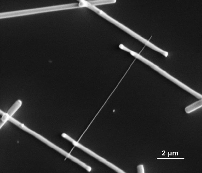
6 Heated Sensors Intoduction Self-heating From random wires to single wire. P 6


7 Heated Sensors Intoduction Self-heating From single wire to random wires??? P 7

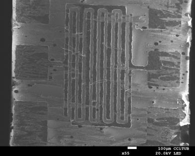
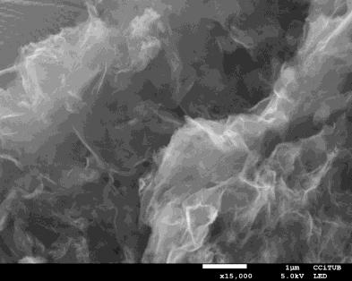
8 Heated Sensors Self-heating in random systems Carbon Nano Fibers (CNF) P 8

9 Heated Sensors Self-heating in random systems Carbon Nano Fibers (CNF) P 9

 P 14 --- 20")
10 Heated Sensors Self-heating in random wires Self-heating in random wires Carbon Nano Fibers (CNF) Sens. Actuators B 187, 401 (2013) P nm m
11 Heated Sensors Self-heating in random systems Self-heating in random CNFs Power consumption? Sens. Actuators B 211, 489 (2015) P 15 Heater operation x10000 x100 Self-heating Significant Power Savings efficient self-heating


12 Counts (--) Heated Sensors Self-heating in random systems Self-heating in random CNFs Origin of efficient heating? Nanoscale 8, 5082 (2016) P 16 Dr. Sauerwald Prof. Schütze Heater operation Heater at 100 C Self-heating at equivalent resistance Hot-spots Self-heating Temperature ( C)

13 Heated Sensors Self-heating in random systems Self-heating in random CNFs Origin of efficient heating? Nanoscale 8, 5082 (2016) P 18 IR Thermography Raman Shift Mapping Hot-spots Hot-spots

14 Heated Sensors Self-heating in random systems Self-heating in random CNFs Origin of hot-spots? Nanoscale 8, 5082 (2016) P 19 τ A << 1 ms τ B ~ 1 s

 P 20 Hot")
15 Heated Sensors Self-heating in random systems Self-heating in random CNFs Resistor network model Nanoscale 8, 5082 (2016) P 20 Hot -spots
16 Heated Sensors Self-heating in random systems Self-heating in random CNFs Resistor network model Nanoscale 8, 5082 (2016) P 21 High Resistance -spots
17 Heated Sensors Self-heating in random systems Self-heating in random CNFs Resistor network model Nanoscale 8, 5082 (2016) P 22 Sensing Resistance -spots
 P 23 Hot -spots High Resistance -spots Sensing Resistance")
18 Heated Sensors Self-heating in random systems Self-heating in random CNFs Validation Nanoscale 8, 5082 (2016) P 23 Hot -spots High Resistance -spots Sensing Resistance -spots

 P 24 Heater operation x10000 x100")
19 Heated Sensors Self-heating in random systems Self-heating in random CNFs Power consumption? Sens. Actuators B 211, 489 (2015) Nanoscale 8, 5082 (2016) P 24 Heater operation x10000 x100 Self-heating

 Continuous")
20 Heated Sensors Pulsed self-heating in random systems P 25 Self-heating in random CNFs Pulsed operation? Sens. Actuators B 226, 254 (2016) Continuous operation Pulsed operation
21 Heated Sensors Pulsed self-heating in random systems P 26 Self-heating in random CNFs Advantages of pulsing Sens. Actuators B 226, 254 (2016) Pulsed-selfheating? 1) Baseline stabiliz.


22 Heated Sensors Self-heating in random systems Self-heating in random nanosystems Is it possible with other materials? P 29 + Materials: + Carbon nanofibers + Carbon nanotubes + Graphene + ZnO nanowires + TiO 2 nanowires + WO 3 nanowies + SnO 2 nanowires + Ge nanowires + Pt nanowires + Methods: + In-situ CVD growth + In-situ hydrothermal + Drop-casting + Electrospray + Dielectrophoresis + Langmuir Blodgett


23 Heated Sensors Self-heating in random systems P 35 Self-heating in random MOX Is it possible with other materials? Yes, and tricks depend on the material used.


24 Illuminated Gas Sensors P 36
![response S(%) [NO 2 ] (ppm) Illumin. Sensors Intoduction Light Activated Gas Sensors Concept Phys.](/docs-images/91/106930923/images/25-1.jpg "Chem.Chem.Phys. 11, 10881 (2009) Sens Actuators B 140, 337 (2009) P 37 100 UV - OFF (T=25ºC) 10 50 1 0 100 50 UV - ON (T=25ºC) 0.1 10 1 0.")
25 response S(%) [NO 2 ] (ppm) Illumin. Sensors Intoduction Light Activated Gas Sensors Concept Phys.Chem.Chem.Phys. 11, (2009) Sens Actuators B 140, 337 (2009) P UV - OFF (T=25ºC) UV - ON (T=25ºC) time (minutes)
 Sens Actuators B 140, 337 (2009) P 38")
26 Illumin. Sensors Intoduction Light Activated Gas Sensors Features Phys.Chem.Chem.Phys. 11, (2009) Sens Actuators B 140, 337 (2009) P 38

 Surface sensitization CdS Absorption (a.")
 Light, ZnO 85 84 0 1 Time (h) 2 400 38 300 200 37 100")
27 Illumin. Sensors Surface Modifications Visible light operation EU-Patent Nr Nano Energy 2, 514 (2013) Surface sensitization CdS Absorption (a.u.) P 39 ZnO/p-Si CdS@ZnO/p-Si nm ZnO Wavelengh (nm) Light, ZnO Time (h) Time (h) 6 [Methane] (ppm) VOC (mv) VOC (mv) [Methane] (ppm) Light, CdS@ZnO


28 Illumin. Sensors Surface Modifications Visible light operation Surface functionalization P 40 Adv. Funct. Mater. 24, 595 (2014)


29 S (%) S (%) S (%) S (%) Illumin. Sensors Visible light operation Surface Modifications Flexibility Adv. Funct. Mater. 24, 595 (2014) P ppm NO ppm EtOH 100 ppm NH 3 4 ppm SO ppm NO ppm EtOH 100 ppm NH 3 4 ppm SO Time (s) Time (s) ppm NO ppm EtOH 100 ppm NH 3 4 ppm SO NO 2, 0.4 ppm NH 3, 100 ppm EtOH, 200 ppm SO 2, 4 ppm CO, 200 ppm Time (s) Time (s)


30 Illumin. Sensors Visible light operation Surface Modifications Selectivity? Adv. Funct. Mater. 24, 595 (2014) P 42 + Good sensitivity + Very good selectivity

31 Illumin. Sensors Monolithic integration Light operated sensors Practical issues P 43 + Poor photon flow control + Distance - geometry + Only current-controlled + High power consumption + Optical loses + >>10mW

32 Illumin. Sensors Monolithic integration Light operated sensors From discret components to monolithic P 44 LED IDE


 n-led p-led SiO 2")
33 Illumin. Sensors Monolithic integration Monolithic integration Sensor platform: In:GaN LED + IDE FET Open 2016 P 45 Sensor Electrodes (IDE) n-led p-led SiO 2 Semi-transp. p electrode p-gan InGaN/GaN MQW n-gan sapphire

34 Illumin. Sensors Monolithic integration Monolithic integration Sensor platform: In:GaN LED + IDE P 46 Sensor material Au semi-transparent p-led IDE SiO 2 InGaN/GaN MQW p-gan n-gan buffer-gan Sapphire n-led


35 Illumin. Sensors Monolithic integration Monolithic integration Results: semi-transparent device P 48 n-led IDE p-led IDE 1 mm


36 P (W) Illumin. Sensors Monolithic integration Monolithic integration Results: P-V characteristics P E-3 1E-4 V = 3.5V I = 246 µa P = 861 µw V Th = 2.82V I th = 19.3µA P Th = 54.4 µw 1E V (V)
37 R (k ) P LED (W) Illumin. Sensors Monolithic integration Monolithic integration Results: efficiency P 53 + CNT photocondutivity activation ,1 0, E-3 1E E Time (min) This work V LED = 2.82 V I LED = 19.3 µa P Th = 54.4 µw Distance ~ 200 nm Commercial LED V LED = 2.95V I LED = 100 ma P Th = 295 mw Distance < 5mm


38 response S (%) Illumin. Sensors Monolithic integration Monolithic integration Result: equivalent responses P mid flux HEATER 10 LIGHT low flux unexcited 1 high flux 0, [NO 2 ] (ppm)
39 Conclusions Heated sensors P 57 Efficient self-heating in random nanostructures Hot - spots High Resistance - spots Sensing Resistance - spots Pulsed - selfheating 1) Baseline stabilization 2) More power savings 3) Faster times As good at sensing as the material used. Can be applied to 1D, 2D, carbon, MOXs.
40 Conclusions Illuminated sensors P 58 Potentially equivalent to heated sensors Surface modification for Visible operation Better Selectivity Practical issue: light control Monolithic integration of LED+IDE: Full light control, lots of power savings Ready to use!


41 END Thank you P 62 + J. Samà + P. García-Lebière + O. Monereo + S. Illera + N. García-Castelló + J. Llosa + A. Varea + E. Xuriguera + R. Jiménez-Díaz + A. Romano-Rodríguez + A. Cirera + A. Cornet + M.W. Hoffmann + A.E. Gad + J. Hartmann + X. Wang + H. Shen + A. Waag + T. Sauerwald + A. Schütze + F. Shao + M. Manzanares + T. Andreu + F. Hernández + S. Barth The research leading to these results has received funding from the European Research Council under the European Union's Seventh Framework Programme (FP/ ) / ERC Grant Agreement n
Parallel Alignment of Nanowires for Fast Fabrication of Nanowire Based Gas Sensors
 Parallel Alignment of Nanowires for Fast Fabrication of Nanowire Based Gas Sensors R. Jiménez-Díaz 1, J.D. Prades 1 F. Hernández-Ramírez, J. Santander 3 C. Calaza 3, L. Fonseca 3, C. Cané 3 A. Romano-Rodriguez
Nanoscale ARTICLE. Localized self-heating in large arrays of 1D nanostructures. Introduction. Please do not adjust margins
 Nanoscale Localized self-heating in large arrays of 1D nanostructures Received 00th January 20xx, Accepted 00th January 20xx DOI: 10.1039/x0xx00000x www.rsc.org/ O. Monereo, a S. Illera, a A. Varea, a
Selective improvement of NO 2 gas sensing behavior in. SnO 2 nanowires by ion-beam irradiation. Supporting Information.
 Supporting Information Selective improvement of NO 2 gas sensing behavior in SnO 2 nanowires by ion-beam irradiation Yong Jung Kwon 1, Sung Yong Kang 1, Ping Wu 2, *, Yuan Peng 2, Sang Sub Kim 3, *, Hyoun
Available online at ScienceDirect. Procedia Engineering 168 (2016 ) th Eurosensors Conference, EUROSENSORS 2016
 th Eurosensors Conference, EUROSENSORS 2016") Available online at www.sciencedirect.com ScienceDirect Procedia Engineering 168 (2016 ) 1056 1060 30th Eurosensors Conference, EUROSENSORS 2016 Site-selectively grown p-type Ge NWs as a gas sensor J.
Available online at www.sciencedirect.com ScienceDirect Procedia Engineering 168 (2016 ) 1056 1060 30th Eurosensors Conference, EUROSENSORS 2016 Site-selectively grown p-type Ge NWs as a gas sensor J.
Contents. Nano-2. Nano-2. Nanoscience II: Nanowires. 2. Growth of nanowires. 1. Nanowire concepts Nano-2. Nano-2
 Contents Nanoscience II: Nanowires Kai Nordlund 17.11.2010 Faculty of Science Department of Physics Division of Materials Physics 1. Introduction: nanowire concepts 2. Growth of nanowires 1. Spontaneous
Introduction to Optoelectronic Devices
 Introduction to Optoelectronic Devices Dr. Jing Bai Assistant Professor Department of Electrical and Computer Engineering University of Minnesota Duluth October 30th, 2012 1 Outline What is the optoelectronics?
Supporting Information
 Supporting Information Robust Pitaya-Structured Pyrite as High Energy Density Cathode for High Rate Lithium Batteries Xijun Xu,, Jun Liu,,,* Zhengbo Liu,, Jiadong Shen,, Renzong Hu,, Jiangwen Liu,, Liuzhang
Current Optics Research at the ElectroOptics Research Institute & Nanotechnology Center
 Current Optics Research at the ElectroOptics Research Institute & Nanotechnology Center Robert W. Cohn, Director ElectroOptics Research Institute & Nanotechnology Center University of Louisville ElectroOptics
write-nanocircuits Direct-write Jaebum Joo and Joseph M. Jacobson Molecular Machines, Media Lab Massachusetts Institute of Technology, Cambridge, MA
 Fab-in in-a-box: Direct-write write-nanocircuits Jaebum Joo and Joseph M. Jacobson Massachusetts Institute of Technology, Cambridge, MA April 17, 2008 Avogadro Scale Computing / 1 Avogadro number s? Intel
Supplementary Information. Highly conductive and flexible color filter electrode using multilayer film
 Supplementary Information Highly conductive and flexible color filter electrode using multilayer film structure Jun Hee Han 1, Dong-Young Kim 1, Dohong Kim 1, and Kyung Cheol Choi 1,* 1 School of Electrical
Chalcogenide Memory, Logic and Processing Devices. Prof C David Wright Department of Engineering University of Exeter
 Chalcogenide Memory, Logic and Processing Devices Prof C David Wright Department of Engineering University of Exeter (david.wright@exeter.ac.uk) Acknowledgements University of Exeter Yat-Yin Au, Jorge
Low Energy Nanolayer Sensors. Thermal reactivation
 Low Energy Nanolayer Sensors W. Moritz 1, M. Milstrey 2 1 Humboldt University of Berlin, Brook-Taylor-Str.2, 12489 Berlin, Germany; email: werner.moritz@rz.hu-berlin.de 2 Swissbit Germany AG Sensor structure
Synthesis of nanowires and nanotubes
 Synthesis of nanowires and nanotubes Laser-assisted Catalytic Growth Source target with catalyst is evaporated by laser. Nanomaterials are collected on a cold finger. Synthesized semiconductor NWs - Si,
Light management in photovoltaics using nanotechnology
 Light management in photovoltaics using nanotechnology Albert Polman Center for Nanophotonics FOM-Institute AMOLF Amsterdam, The Netherlands Solar irradiance on earth assuming 30% PV, 175 W/m 2 Solar
Bottom-up Nanostructures just a research hype?
 Fakultät Maschinenwesen, Institut für Werkstoffwissenschaft, Professur Materialwissenschaft u. Nanotechnik Bottom-up Nanostructures just a research hype? Dr.-Ing. Alexander Nerowski Dresden, 22.09.2017
Photonic Crystal Slot Waveguide Spectrometer for Detection of Methane
 Photonic Crystal Slot Waveguide Spectrometer for Detection of Methane Swapnajit Chakravarty 1, Wei-Cheng Lai 2, Xiaolong (Alan) Wang 1, Che-Yun Lin 2, Ray T. Chen 1,2 1 Omega Optics, 10306 Sausalito Drive,
Zinc Oxide Nanowires Impregnated with Platinum and Gold Nanoparticle for Ethanol Sensor
 CMU. J.Nat.Sci. Special Issue on Nanotechnology (2008) Vol. 7(1) 185 Zinc Oxide Nanowires Impregnated with Platinum and Gold Nanoparticle for Ethanol Sensor Weerayut Wongka, Sasitorn Yata, Atcharawan Gardchareon,
S.Vidhya by, Published 4 Feb 2014
 A Wearable And Highly Sensitive Pressure Sensor With Ultrathin Gold Nanowires Shu Gong1,2, Willem Schwalb3, Yongwei Wang1,2, Yi Chen1, Yue Tang1,2, Jye Si1, Bijan Shirinzadeh3 & Wenlong Cheng1,2 1 Department
Design, Fabrication, Characterization, and Application of Semiconductor Nanocomposites
 Design, Fabrication, Characterization, and Application of Semiconductor Nanocomposites Yang-Fang Chen Department of Physics, National Taiwan University, Taipei, Taiwan 1 I. A perfect integration of zero
MINIATURE X-RAY TUBES UTILIZING CARBON-NANOTUBE- BASED COLD CATHODES
 Copyright JCPDS - International Centre for Diffraction Data 25, Advances in X-ray Analysis, Volume 48. 24 MINIATURE X-RAY TUBES UTILIZING CARBON-NANOTUBE- BASED COLD CATHODES A. Reyes-Mena, Charles Jensen,
Sub 300 nm Wavelength III-Nitride Tunnel-Injected Ultraviolet LEDs
 Sub 300 nm Wavelength III-Nitride Tunnel-Injected Ultraviolet LEDs Yuewei Zhang, Sriram Krishnamoorthy, Fatih Akyol, Sadia Monika Siddharth Rajan ECE, The Ohio State University Andrew Allerman, Michael
Monolithically Integrated Thin-Film/Si Tandem Photoelectrodes
 Monolithically Integrated Thin-Film/Si Tandem Photoelectrodes Author Name: Zetian Mi Date: November 14, 2017 Venue: NREL s Energy Systems Integration Facility HydroGEN Kick-Off Meeting MONOLITHICALLY INTEGRATED
SYNTHESIS AND ANALYSIS OF SILICON NANOWIRES GROWN ON Si (111) SUBSTRATE AT DIFFERENT SILANE GAS FLOW RATE
 SUBSTRATE AT DIFFERENT SILANE GAS FLOW RATE") SYNTHESIS AND ANALYSIS OF SILICON NANOWIRES GROWN ON Si (111) SUBSTRATE AT DIFFERENT SILANE GAS FLOW RATE Habib Hamidinezhad*, Yussof Wahab, Zulkafli Othaman and Imam Sumpono Ibnu Sina Institute for Fundamental
SYNTHESIS AND ANALYSIS OF SILICON NANOWIRES GROWN ON Si (111) SUBSTRATE AT DIFFERENT SILANE GAS FLOW RATE Habib Hamidinezhad*, Yussof Wahab, Zulkafli Othaman and Imam Sumpono Ibnu Sina Institute for Fundamental
Synthesis of Silicon. applications. Nanowires Team. Régis Rogel (Ass.Pr), Anne-Claire Salaün (Ass. Pr)
, Anne-Claire Salaün (Ass. Pr)") Synthesis of Silicon nanowires for sensor applications Anne-Claire Salaün Nanowires Team Laurent Pichon (Pr), Régis Rogel (Ass.Pr), Anne-Claire Salaün (Ass. Pr) Ph-D positions: Fouad Demami, Liang Ni,
Synthesis of Silicon nanowires for sensor applications Anne-Claire Salaün Nanowires Team Laurent Pichon (Pr), Régis Rogel (Ass.Pr), Anne-Claire Salaün (Ass. Pr) Ph-D positions: Fouad Demami, Liang Ni,
P-CUBE-Series High Sensitivity PIN Detector Modules
 High Sensitivity PIN Detector Modules Description The P-CUBE-series manufactured by LASER COMPONENTS has been designed for customers interested in experimenting with low noise silicon or InGaAs pin detectors.
Nanophotonics: Single-nanowire electrically driven lasers
 Nanophotonics: Single-nanowire electrically driven lasers Ivan Stepanov June 19, 2010 Single crystaline nanowires have unique optic and electronic properties and their potential use in novel photonic and
Thermal Management in the 3D-SiP World of the Future
 Thermal Management in the 3D-SiP World of the Future Presented by W. R. Bottoms March 181 th, 2013 Smaller, More Powerful Portable Devices Are Driving Up Power Density Power (both power delivery and power
Near/Mid-Infrared Heterogeneous Si Photonics
 PHOTONICS RESEARCH GROUP Near/Mid-Infrared Heterogeneous Si Photonics Zhechao Wang, PhD Photonics Research Group Ghent University / imec, Belgium ICSI-9, Montreal PHOTONICS RESEARCH GROUP 1 Outline Ge-on-Si
Department of Electrical Engineering and Computer Science, Massachusetts Institute of Technology, 77. Table of Contents 1
 Efficient single photon detection from 500 nm to 5 μm wavelength: Supporting Information F. Marsili 1, F. Bellei 1, F. Najafi 1, A. E. Dane 1, E. A. Dauler 2, R. J. Molnar 2, K. K. Berggren 1* 1 Department
Directly Printed Wearable Electronic Sensing Textiles towards
 Electronic Supplementary Material (ESI) for Journal of Materials Chemistry C. This journal is The Royal Society of Chemistry 2018 Supplementary Information for Directly Printed Wearable Electronic Sensing
Highly efficient SERS nanowire/ag composites
 Highly efficient SERS nanowire/ag composites S.M. Prokes, O.J. Glembocki and R.W. Rendell Electronics Science and Technology Division Introduction: Optically based sensing provides advantages over electronic
Opportunities and Challenges for Nanoelectronic Devices and Processes
 The Sixth U.S.-Korea Forum on Nanotechnology, April 28-29, 2009, Las Vegas, NV Opportunities and Challenges for Nanoelectronic Devices and Processes Yoshio Nishi Professor, Electrical Engineering, Material
Supporting Information. A Tough and High-Performance Transparent Electrode from a. Scalable Transfer-Free Method
 Supporting Information A Tough and High-Performance Transparent Electrode from a Scalable Transfer-Free Method Tianda He, Aozhen Xie, Darrell H. Reneker and Yu Zhu * Department of Polymer Science, College
SUPPLEMENTARY INFORMATION
 SUPPLEMENTARY INFORMATION Self-powered Nanowire Devices Sheng Xu#, Yong Qin#, Chen Xu#, Yaguang Wei, Rusen Yang, Zhong Lin Wang # Authors with equal contribution Self-powered system A totally self-powered
Microfiber- Nanowire Hybrid Structure for Energy Scavenging
 Supplementary materials Microfiber- Nanowire Hybrid Structure for Energy Scavenging Yong Qin#, Xudong Wang# and Zhong Lin Wang* School of Materials Science and Engineering, Georgia Institute of Technology,
Microprobe-enabled Terahertz sensing applications
 Microprobe-enabled Terahertz sensing applications World of Photonics, Laser 2015, Munich Protemics GmbH Aachen, Germany Terahertz microprobing technology: Taking advantage of Terahertz range benefits without
Nanostrukturphysik (Nanostructure Physics)
") Nanostrukturphysik (Nanostructure Physics) Prof. Yong Lei & Dr. Yang Xu Fachgebiet 3D-Nanostrukturierung, Institut für Physik Contact: yong.lei@tu-ilmenau.de; yang.xu@tu-ilmenau.de Office: Unterpoerlitzer
Nanostrukturphysik (Nanostructure Physics) Prof. Yong Lei & Dr. Yang Xu Fachgebiet 3D-Nanostrukturierung, Institut für Physik Contact: yong.lei@tu-ilmenau.de; yang.xu@tu-ilmenau.de Office: Unterpoerlitzer
Micro Analytical Instruments - A System Approach. Jörg Müller Institut für Mikrosystemtechnik
 Micro Analytical Instruments - A System Approach Jörg Müller Institut für Mikrosystemtechnik Technische h Universität i Hamburg-Harburg H b Outline Motivation Political Political Issues Design Principles
Integration of Metal Oxide Nanowires in Flexible Gas Sensing Devices
 Sensors 2013, 13, 10659-10673; doi:10.3390/s130810659 Review OPEN ACCESS sensors ISSN 1424-8220 www.mdpi.com/journal/sensors Integration of Metal Oxide Nanowires in Flexible Gas Sensing Devices Elisabetta
Monolithic photonic integration of suspended light emitting diode,
 Monolithic photonic integration of suspended light emitting diode, waveguide and photodetector Yongjin Wang 1, *, Dan Bai 1, Xumin Gao 1, Wei Cai 1, Yin Xu 1, Jialei Yuan 1, Guixia Zhu 1, Yongchao Yang
SUPPLEMENTARY INFORMATION
 In the format provided by the authors and unedited. Photon-triggered nanowire transistors Jungkil Kim, Hoo-Cheol Lee, Kyoung-Ho Kim, Min-Soo Hwang, Jin-Sung Park, Jung Min Lee, Jae-Pil So, Jae-Hyuck Choi,
Supplementary materials for Tactile Feedback Display with Spatial and Temporal Resolutions
 Supplementary materials for Tactile Feedback Display with Spatial and Temporal Resolutions Siarhei Vishniakou,, Brian W. Lewis,, Xiaofan Niu, Alireza Kargar, Ke Sun, Michael Kalajian,, Namseok Park, Muchuan
Advancing Consumer Packaging Through Printable Electronics
 IPST Executive Conference, Atlanta, GA March 9-10, 2011 Advancing Consumer Packaging Through Printable Electronics Bernard Kippelen Professor, School of Electrical and Computer Engineering Director, Center
Nanoscale switching in resistive memory structures
 Nanoscale switching in resistive memory structures D. Deleruyelle, C. Dumas, M. Carmona, Ch. Muller IM2NP UMR CNRS 6242 & Institut Carnot STAR Polytech Marseille, Université de Provence IMT Technopôle
Carbon Nanotube Radiometer for Cryogenic Calibrations
 Carbon Nanotube Radiometer for Cryogenic Calibrations Solomon I. Woods a, Julia K. Scherschligt a, Nathan A. Tomlin b, John H. Lehman b a National Institute of Standards and Technology, 100 Bureau Drive,
Low Temperature Integration of Thin Films and Devices for Flexible and Stretchable Electronics
 Low Temperature Integration of Thin Films and Devices for Flexible and Stretchable Electronics Pooran Joshi, Stephen Killough, and Teja Kuruganti Oak Ridge National Laboratory FIIW 2015 Displays and PV
Carbon Nanotube Bumps for Thermal and Electric Conduction in Transistor
 Carbon Nanotube Bumps for Thermal and Electric Conduction in Transistor V Taisuke Iwai V Yuji Awano (Manuscript received April 9, 07) The continuous miniaturization of semiconductor chips has rapidly improved
Add CLUE to your SEM. High-efficiency CL signal-collection. Designed for your SEM and application. Maintains original SEM functionality
 Add CLUE to your SEM Designed for your SEM and application The CLUE family offers dedicated CL systems for imaging and spectroscopic analysis suitable for most SEMs. In addition, when combined with other
Metal Oxide Nanowires: : Synthesis, Characterization and Device Applications
 Metal Oxide Nanowires: : Synthesis, Characterization and Device Applications Jia Grace Lu Dept. of Chemical Engineering and Materials Science & Dept. of Electrical Engineering and Computer Science University
Nanoscale relative emission efficiency mapping using cathodoluminescence g (2) imaging
 imaging") Supplementary information Nanoscale relative emission efficiency mapping using cathodoluminescence g (2) imaging Sophie Meuret 1 *, Toon Coenen 1,2, Steffi Y. Woo 3, Yong Ho Ra 4,5, Zetian Mi 4,6, Albert
Supplementary information Nanoscale relative emission efficiency mapping using cathodoluminescence g (2) imaging Sophie Meuret 1 *, Toon Coenen 1,2, Steffi Y. Woo 3, Yong Ho Ra 4,5, Zetian Mi 4,6, Albert
Embedded System Design and Synthesis. Transition. Evolution of computation. Two major sources of changing problems. Impact of scaling on delay
 Transition http://robertdick.org/esds/ Office: EECS 2417-E Department of Electrical Engineering and Computer Science University of Michigan Classes will transition from covering background on embedded
Detecting single photons. Andrea Fiore
 Detecting single photons Why single-photon detectors? Measure "very efficient" nonlinear frequency conversion... A PhD student "under Rosencher's rule": Will I ever get a few photons and my thesis? Wikipedia
Solution-Processed Metal Nanowire Mesh Transparent Electrodes
 Letter Subscriber access provided by STANFORD UNIV GREEN LIBR Solution-Processed Metal Nanowire Mesh Transparent Electrodes Jung-Yong Lee, Stephen T. Connor, Yi Cui, and Peter Peumans Nano Lett., 2008,
Waveguide superconducting single-photon detectors for Integrated Quantum Photonic devices
 Waveguide superconducting single-photon detectors for Integrated Quantum Photonic devices KOBIT- 1 Izmir Yuksek Teknoloji Enstitusu Döndü Sahin QET Labs, d.sahin@bristol.ac.uk EU-FP7 Implementing QNIX
NEXT GENERATION SILICON PHOTONICS FOR COMPUTING AND COMMUNICATION PHILIPPE ABSIL
 NEXT GENERATION SILICON PHOTONICS FOR COMPUTING AND COMMUNICATION PHILIPPE ABSIL OUTLINE Introduction Platform Overview Device Library Overview What s Next? Conclusion OUTLINE Introduction Platform Overview
Photoconduction studies on GaN nanowire transistors under UV and polarized UV illumination
 Chemical Physics Letters 389 (24) 176 18 www.elsevier.com/locate/cplett Photoconduction studies on GaN nanowire transistors under UV and polarized UV illumination Song Han, Wu Jin, Daihua Zhang, Tao Tang,
Micro-sensors - what happens when you make "classical" devices "small": MEMS devices and integrated bolometric IR detectors
 Micro-sensors - what happens when you make "classical" devices "small": MEMS devices and integrated bolometric IR detectors Dean P. Neikirk 1 MURI bio-ir sensors kick-off 6/16/98 Where are the targets
National Science Foundation Center for Lasers and Plasmas for Advanced Manufacturing. Mool C. Gupta Applied Research Center Old Dominion University
 National Science Foundation Center for Lasers and Plasmas for Advanced Manufacturing Mool C. Gupta Applied Research Center Old Dominion University National Science Foundation Center - Center Mission -
The European Sensor-Systems Cluster (ESSC): High Impact EC Initiative on Sensor Technologies for Sustainable Applications
: High Impact EC Initiative on Sensor Technologies for Sustainable Applications") The European Sensor-Systems Cluster (ESSC): High Impact EC Initiative on Sensor Technologies for Sustainable Applications Michele Penza Chairman of ESSC & Chair of COST Action TD1105 ENEA, Brindisi, Italy
The European Sensor-Systems Cluster (ESSC): High Impact EC Initiative on Sensor Technologies for Sustainable Applications Michele Penza Chairman of ESSC & Chair of COST Action TD1105 ENEA, Brindisi, Italy
Fabrication of High-Speed Resonant Cavity Enhanced Schottky Photodiodes
 Fabrication of High-Speed Resonant Cavity Enhanced Schottky Photodiodes Abstract We report the fabrication and testing of a GaAs-based high-speed resonant cavity enhanced (RCE) Schottky photodiode. The
SUPERCONDUCTING NANOTECHNOLOGY
 SUPERCONDUCTING NANOTECHNOLOGY Detect everything you want I.TECHNICAL SPECIFICATION OF TERAHERTZ DETECTION SYSTEMS Product description: The Terahertz detection systems are optimized for three frequency
MoS 2 nanosheet phototransistors with thicknessmodulated
 Supporting Information MoS 2 nanosheet phototransistors with thicknessmodulated optical energy gap Hee Sung Lee, Sung-Wook Min, Youn-Gyung Chang, Park Min Kyu, Taewook Nam, # Hyungjun Kim, # Jae Hoon Kim,
Preamplifier shaper: The preamplifier. The shaper. The Output.
 Preamplifier shaper: In previous simulations I just tried to reach the speed limits. The only way to realise this was by using a lot of current, about 1 ma through the input transistor. This gives in the
Carbon Nanotubes and Oxide Nanowires: Synthesis, Properties and Applications Koungmin Ryu
 Carbon Nanotubes and Oxide Nanowires: Synthesis, Properties and Applications Koungmin Ryu Advisor : Prof. Chongwu Zhou Ming Hsieh Dept. of Electrical Engineering Viterbi School of Engineering University
Silicon Carbide Solid-State Photomultiplier for UV Light Detection
 Silicon Carbide Solid-State Photomultiplier for UV Light Detection Sergei Dolinsky, Stanislav Soloviev, Peter Sandvik, and Sabarni Palit GE Global Research 1 Why Solid-State? PMTs are sensitive to magnetic
Increasing the Sensitivity and Selectivity of Metal Oxide Gas Sensors by Controlling the Sensitive Layer Polarization
 Increasing the Sensitivity and Selectivity of Metal Oxide Gas Sensors by Controlling the Sensitive Layer Polarization Nicolas Dufour, Yoan Veyrac, Philippe Menini, Frédéric Blanc, Chabane Talhi, Bernard
NanoOptics: Illuminating Nanostructures
 NanoOptics: Illuminating Nanostructures Martin Moskovits Chief Technology Officer, API Nanotronics Corp. 2009 International Conference on Nanotechnology for the Forest Products Industry Edmonton, Alberta,
Steps towards a GaN nanowire based light emitting diode and its integration with Si-MOS technology
 Steps towards a GaN nanowire based light emitting diode and its integration with Si-MOS technology Friederich Limbach 1/33 Motivation Monolithic integration of III-V optoelectronic devices with Si based
(PT-3528) Chip Ambient Light Sensor, RoHS Compliant. Token Electronics Industry Co., Ltd. Version: July 26, Web:
 Chip Ambient Light Sensor, RoHS Compliant. Token Electronics Industry Co., Ltd. Version: July 26, Web:") Version: July 26, 2017 (PT-3528) Chip Ambient Light Sensor, RoHS Compliant Token Electronics Industry Co., Ltd. Web: www.token.com.tw Email: rfq@token.com.tw Taiwan: No.137, Sec. 1, Zhongxing Rd., Wugu
Version: July 26, 2017 (PT-3528) Chip Ambient Light Sensor, RoHS Compliant Token Electronics Industry Co., Ltd. Web: www.token.com.tw Email: rfq@token.com.tw Taiwan: No.137, Sec. 1, Zhongxing Rd., Wugu
p-n Junction Diodes Fabricated Using Poly (3-hexylthiophene-2,5-dyil) Thin Films And Nanofibers
 Thin Films And Nanofibers") Proceedings of the National Conference On Undergraduate Research (NCUR) 2017 University of Memphis, TN Memphis, Tennessee April 6 8, 2017 p-n Junction Diodes Fabricated Using Poly (3-hexylthiophene-2,5-dyil)
Proceedings of the National Conference On Undergraduate Research (NCUR) 2017 University of Memphis, TN Memphis, Tennessee April 6 8, 2017 p-n Junction Diodes Fabricated Using Poly (3-hexylthiophene-2,5-dyil)
Photosensitive Gold-Nanoparticle-Embedded Dielectric Nanowires
 Photosensitive Gold-Nanoparticle-Embedded Dielectric Nanowires Ming-Shien Hu 1,2, Hsin-Li Chen 3,4, Ching-Hsing Shen 4, Lu-Sheng Hong 1, Bohr-Ran Huang 3, Kuei-Hsien Chen 2,4 * and Li-Chyong Chen 4 Abstract
Implementation of All-Optical Logic AND Gate using XGM based on Semiconductor Optical Amplifiers
 Implementation of All-Optical Logic AND Gate using XGM based on Semiconductor Optical Amplifiers Sang H. Kim 1, J. H. Kim 1,2, C. W. Son 1, G. Kim 1, Y. T. yun 1, Y. M. Jhon 1, S. Lee 1, D. H. Woo 1, and
Atomristor: Non-Volatile Resistance Switching in Atomic Sheets of
 Atomristor: Non-Volatile Resistance Switching in Atomic Sheets of Transition Metal Dichalcogenides Ruijing Ge 1, Xiaohan Wu 1, Myungsoo Kim 1, Jianping Shi 2, Sushant Sonde 3,4, Li Tao 5,1, Yanfeng Zhang
Components of Optical Instruments
 Components of Optical Instruments General Design of Optical Instruments Sources of Radiation Wavelength Selectors (Filters, Monochromators, Interferometers) Sample Containers Radiation Transducers (Detectors)
Superconducting Nanowire Single Photon Detector (SNSPD) integrated with optical circuits
 integrated with optical circuits") Superconducting Nanowire Single Photon Detector (SNSPD) integrated with optical circuits Marcello Graziosi, ESR 3 within PICQUE (Marie Curie ITN project) and PhD student marcello.graziosi@ifn.cnr.it Istituto
Superconducting Nanowire Single Photon Detector (SNSPD) integrated with optical circuits Marcello Graziosi, ESR 3 within PICQUE (Marie Curie ITN project) and PhD student marcello.graziosi@ifn.cnr.it Istituto
:... resolution is about 1.4 μm, assumed an excitation wavelength of 633 nm and a numerical aperture of 0.65 at 633 nm.
 PAGE 30 & 2008 2007 PRODUCT CATALOG Confocal Microscopy - CFM fundamentals :... Over the years, confocal microscopy has become the method of choice for obtaining clear, three-dimensional optical images
SUPPLEMENTARY INFORMATION
 SUPPLEMENTARY INFORMATION doi: 1.138/nphoton.211.25 Efficient Photovoltage Multiplication in Carbon Nanotubes Leijing Yang 1,2,3+, Sheng Wang 1,2+, Qingsheng Zeng, 1,2, Zhiyong Zhang 1,2, Tian Pei 1,2,
C30659 Series 900/1060/1550/1550E Si and InGaAs APD Preamplifier Modules
 DATASHEET Photon Detection C3659 Series 9/6/15/15E Excelitas C3659-15E InGaAs APD Preamplifier Modules exhibit enhanced damage threshold and greater resilience when exposed to higher optical power densities.
Monitoring of Galvanic Replacement Reaction. between Silver Nanowires and HAuCl 4 by In-Situ. Transmission X-Ray Microscopy
 Supporting Information Monitoring of Galvanic Replacement Reaction between Silver Nanowires and HAuCl 4 by In-Situ Transmission X-Ray Microscopy Yugang Sun *, and Yuxin Wang Center for Nanoscale Materials
Supplementary Figure 1: Electron and hole distribution in a 100 nm diameter In 0.25 Ga 0.75 N
 Supplementary Figure 1: Electron and hole distribution in a 100 nm diameter In 0.25 Ga 0.75 N nanowire in the presence of ~0.37 ev upward surface band bending (inset) under certain excitation conditions.
Characterisation of New Planar Cryogenic Radiometric Standards under Development at NIST
 Characterisation of New Planar Cryogenic Radiometric Standards under Development at NIST Malcolm White CALCON 2016 National Institute of Standards and Technology 325 Broadway, Boulder, Colorado 80305-3228
DTU DANCHIP an open access micro/nanofabrication facility bridging academic research and small scale production
 DTU DANCHIP an open access micro/nanofabrication facility bridging academic research and small scale production DTU Danchip National Center for Micro- and Nanofabrication DTU Danchip DTU Danchip is Denmark
Ultra-Low Power Analog Sensor Module for Sulfur Dioxide
 Ultra-Low Power Analog Sensor Module for Sulfur Dioxide BENEFITS 0 to 3 V Analog Signal Output Low Power Consumption < 45 µw Fast Response On-board Temperature Sensor Easy Sensor Replacement Standard 8-pin
High Intensity LumiBright LE LED Light Engine
 HIGH BRIGHTNESS LED PACKAGES AND OPTICAL SYSTEM SOLUTIONS High Intensity LumiBright LE LED Light Engine Standard Features: Highest Brightness light engine. UV thru near IR. Uniform Near and Far Fields.
An application of electron beam lithography: location of metallic nanostructures based on. Enrique Samano CNyN-UNAM, Ensenada, B.C.
 About OMICS Group OMICS Group International is an amalgamation of Open Access publications and worldwide international science conferences and events. Established in the year 2007 with the sole aim of
High Performance Visible-Blind Ultraviolet Photodetector Based on
 Supplementary Information High Performance Visible-Blind Ultraviolet Photodetector Based on IGZO TFT Coupled with p-n Heterojunction Jingjing Yu a,b, Kashif Javaid b,c, Lingyan Liang b,*, Weihua Wu a,b,
High Energy Density Asymmetric Quasi-Solid-State Supercapacitor Based on Porous Vanadium Nitride Nanowire Anode
 pubs.acs.org/nanolett High Energy Density Asymmetric Quasi-Solid-State Supercapacitor Based on Porous Vanadium Nitride Nanowire Anode Xihong Lu,, Minghao Yu, Teng Zhai, Gongming Wang, Shilei Xie, Tianyu
Industrial Innovation Information Days Brussels 3-4 October 2017
 Industrial Innovation Information Days Brussels 3-4 October 2017 NMBP Programme Parallel Sessions OPEN INNOVATION TEST BEDS Calls 2018/2019 Helene CHRAYE, HoU Unit D3 DG Research & Innovation A joint presentation
A 3.9 ns 8.9 mw 4 4 Silicon Photonic Switch Hybrid-Integrated with CMOS Driver
 A 3.9 ns 8.9 mw 4 4 Silicon Photonic Switch Hybrid-Integrated with CMOS Driver A. Rylyakov, C. Schow, B. Lee, W. Green, J. Van Campenhout, M. Yang, F. Doany, S. Assefa, C. Jahnes, J. Kash, Y. Vlasov IBM
This Week s Subject. DRAM & Flexible RRAM. p-channel MOSFET (PMOS) CMOS: Complementary Metal Oxide Semiconductor
 CMOS: Complementary Metal Oxide Semiconductor") DRAM & Flexible RRAM This Week s Subject p-channel MOSFET (PMOS) CMOS: Complementary Metal Oxide Semiconductor CMOS Logic Inverter NAND gate NOR gate CMOS Integration & Layout GaAs MESFET (JFET) 1 Flexible
DRAM & Flexible RRAM This Week s Subject p-channel MOSFET (PMOS) CMOS: Complementary Metal Oxide Semiconductor CMOS Logic Inverter NAND gate NOR gate CMOS Integration & Layout GaAs MESFET (JFET) 1 Flexible
Characterization using laser-based technique for failure Si PV module
 SAYURI-PV, Tsukuba, 4th Oct, 2016 Characterization using laser-based technique for failure Si PV module Y. Ishikawa, 1 M. A. Islam, 1 K. Noguchi, 1 H. Iida, 2 Y. Takagi, 2 and H. Nakahama 2 1: NAIST, 2:
Photo-patternable and Transparent Films Using Cellulose Nanofibers for Stretchable, Origami Electronics
 Supplementary information for Photo-patternable and Transparent Films Using Cellulose Nanofibers for Stretchable, Origami Electronics Sangyoon Ji 1, 4, Byung Gwan Hyun 1, 4, Kukjoo Kim 1, 4, Sang Yun Lee
Chihyun Hwang, Tae-Hee Kim, Yoon-Gyo Cho, Jieun Kim and Hyun-Kon Song*
 Supporting Information All-in-one assembly based on 3D-intertangled and cross-jointed architectures of Si/Cu 1D-nanowires for lithium ion batteries Chihyun Hwang, Tae-Hee Kim, Yoon-Gyo Cho, Jieun Kim and
Ultra High Thermal Conductivity Nanowire Filled Polymer Composites And Interfaces
 Ultra High Thermal Conductivity Nanowire Filled Polymer Composites And Interfaces Indira Seshadri Graduate Research Assistant Department of Materials Science and Engineering Rensselaer Polytechnic Institute,
Nanoscale FEATURE ARTICLE. Transparent metal oxide nanowire transistors. Dynamic Article Links C <
 Nanoscale View Article Online / Journal Homepage / Table of Contents for this issue Dynamic Article Links C < Cite this: Nanoscale, 2012, 4, 3001 www.rsc.org/nanoscale Transparent metal oxide nanowire
ULPSM-Ethanol
 Ultra-Low Power Analog Sensor Module for Ethanol BENEFITS 0 to 3 V Analog Signal Output Low Power Consumption < 45 µw Fast Response On-board Temperature Sensor Easy Sensor Replacement Standard 8-pin connector
Investigating the Electronic Behavior of Nano-materials From Charge Transport Properties to System Response
 Investigating the Electronic Behavior of Nano-materials From Charge Transport Properties to System Response Amit Verma Assistant Professor Department of Electrical Engineering & Computer Science Texas
Energy & Space. International Presentations
 Energy & Space International Presentations 2012-2013 Advanced Electronics 3D Printed Circuit Boards 3D Printed Circuit Boards for Solder-Free Printable Electronics 4x4 Vehicles Arduino WiFi Android Controllers
4.1.2 InAs nanowire circuits fabricated by field-assisted selfassembly on a host substrate
 22 Annual Report 2010 - Solid-State Electronics Department 4.1.2 InAs nanowire circuits fabricated by field-assisted selfassembly on a host substrate Student Scientist in collaboration with R. Richter
Lecture 18: Photodetectors
 Lecture 18: Photodetectors Contents 1 Introduction 1 2 Photodetector principle 2 3 Photoconductor 4 4 Photodiodes 6 4.1 Heterojunction photodiode.................... 8 4.2 Metal-semiconductor photodiode................