Synthesis of nanowires and nanotubes
|
|
|
- Ashley O’Brien’
- 5 years ago
- Views:
Transcription

1 Synthesis of nanowires and nanotubes Laser-assisted Catalytic Growth Source target with catalyst is evaporated by laser. Nanomaterials are collected on a cold finger. Synthesized semiconductor NWs - Si, Ge, GaN, GaAs, GaP, InP, InAs, ZnS, ZnSe, CdS, CdSe NW


2 Synthesis of NWs Thermal chemical vapor deposition P. Yang, Adv. Funct. Mater. 2002, 12, 323 Mixed source powder is evaporated by heating ZnO Nanowire is grown on the Aucoated Si or Sapphire substrate. ZnO is reduced by C to generate Zn vapor.

 V L 2 sd The slopes depend on electron mobility The electron")
3 GaN Nanowire Nanodevice Field effect transistors(fets) based on a GaN nanowire have been fabricated Lieber, Nano lett. 2002, 2, 101 The investigation of the carrier mobility(μ) in these n-type GaN nanowire FETs di dv g C = µ( ) V L 2 sd The slopes depend on electron mobility The electron mobility of nanowire is higher than that of GaN thin film: 소자의응답속도개선
 When a voltage is applied to the silicon nanowire, current runs into each of the crossed wires causing emission of blue, green and red light at the respective crossing points.")
4 Nanoscale Light Emitting Diode (LED) Nature 2001, 409, 66 Multicolor nanowire LED A p-doped Si nanowire (hole) is crossed with three different n-doped (electron) nanowires (GaN, CdS, and InP) When a voltage is applied to the silicon nanowire, current runs into each of the crossed wires causing emission of blue, green and red light at the respective crossing points.

5 Nanowire UV Photodetector and Optical Switches Adv. Mater. 2002, 14, 158 UV Photodetector Reversible optical switch When ZnO nanowires are exposed to UV, resistivity decreases by 4 to 6 orders of magnitude. ON : the UV-exposed conducting state OFF : the insulating state Nanowires can be reversibly switched between the low and high conductivity state.


6 Nanowire nanolasers Science 2001, 292, 1897 Optically pumped nanolaser Schematic drawing <0001> oriented ZnO nanowire arrays LASER Nanolaser Under optical excitation, surfaceemitting lasing action at 385 nm
 는브라운관과유사한원리를이용한 평판디스플레이로,")


7 브라운관의내부구조 벽걸이형 TV(FED) 벽걸이형 TV 내부구조 전자총 전자총 array Metal tip 벽걸이형 TV 를위한전계방출소자 (FED) 는브라운관과유사한원리를이용한 평판디스플레이로, 브라운관의높은휘도, 넓은시야각등의특성을유지하면서, 두께가얇고가볍다는장점을가지고있어차세대디스플레이로서주목받고있다. 이소자의핵심기술은전자총소재의개발인데, 최근기존의금속재료대신, 안정성이 뛰어나고, 전자방출효율이좋은탄소나노튜브및 ZnO 나노선등이신소재로서사용되고있다. 특히 3D TV 의경우좌우눈을위한두개의상을보여주어야하기때문에화면이더 bright 해 야하므로새로운 display 의개발이요구된다. Carbon nanotube tips


8 수직성장된 ZnO 를이용한 FED 제작
 Co 5 Ge 7 NW on graphene")
9 Flexible Field Emission Display (Adv. Mat. 2009) Co 5 Ge 7 NW on graphene

10 Lattice match for the epitaxial growth of Co 5 Ge 7 on graphite


11
12 Field emission current density versus applied electrical field at a working distance of 500 μm. The emission current density is as high as 1.7 ma cm -2 at a field of 2.8 V μm -1, and the turn-on field of the sample is about 1.6 V μm -1. The emission of bare HOPG without NWs shows no FE data. Inset shows a schematic illustration of a field emission experimental setup.
13 Vertical Fe 1.3 Ge NW Arrays Integrated on Few-Layer Graphene for an Effective Field Emitter Good epitaxial lattice match (2.7%) Fe 1.3 Ge NWs (on Graphene) Single-crystalline NW
 (~1580) (~2700) Decreased G band & blue-shifted 2D band; few")
14 Fe 1.3 Ge NWs on Few-layer Graphene & FE property FE of Fe 1.3 Ge NWs (on Graphene) (~1580) (~2700) Decreased G band & blue-shifted 2D band; few graphene layers (3-5).


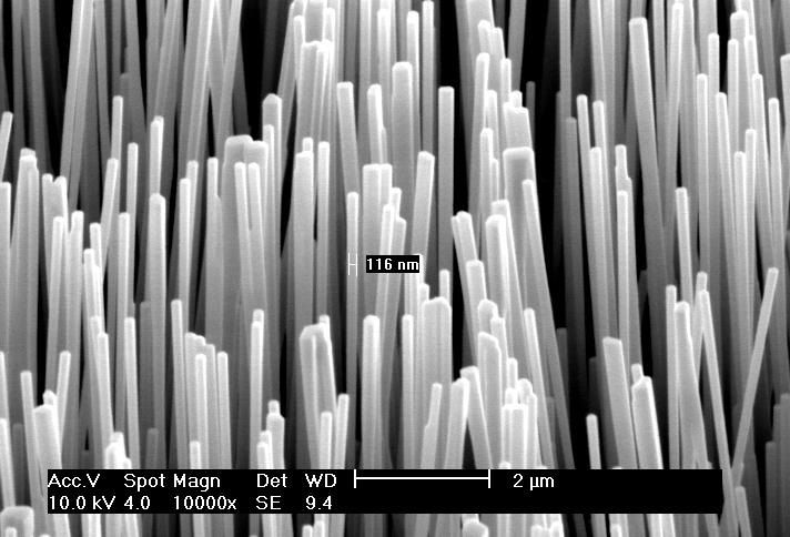
15 Ag NWs synthesized on a sapphire substrate Single crystalline Ag NW SEM image Equivalent to an FFT pattern of a TEM image High-resolution TEM image SAED image (Selected area electron diffraction)


16 MicroRaman 100 배대물렌즈 Excitation source : nm Ar ion laser Laser power : 0.5 mw

17

18

19 Time-Resolved Innovative Nanowire Diffraction Laboratory Center


20 Visualizing SERS Hot Spots by Crossing NWs BCB dye, 514 nm laser

21

 1661.")

22 BCB - Ag nanowire i) Parallel case Intensity (a.u) Wavelength (cm -1 )


23 SERS 의응용 : selective biosensor 1.Thiol is self-assembled on the surface of Ag. 3. 최근상업화된 SERS 기판칩 2. 자기조립된물질의끝에유용한작용기도입 : biotin, SpA(protein), U1A(antigen)


24 2)Single NW on-film as a SERS platform JACS (2009)

25 Reproducibile and Stable SERS signal of SNOF SNOF provides reliable reproducible and highly stable SERS signals.

26 7.Multiplex Pathogen DNA Detection By Au Particle-on-Wire SERS Sensor Nano Lett. (2010) First Multiplex SERS pathogen Diagnosing Sensor
27
.")
28 a) Two Au NWs functionalized with different probe DNAs (Efm and Sau001-20) are incubated in mixed solution of target DNAs (T1 and T2) and immersed into a solution of Au NPs modified with reporter DNAs (R1 and R2). Because R1 and R2 contains Cy5 and TAMRA as a Raman dye, respectively, the upper particle-on-wire structure gives SERS signal of Cy5 and the lower one gives SERS signal of TAMRA, respectively. b) (b) SERS spectra of Cy5 and TAMRA from Au particle-on-wire systems after DNA hybridization. The inset is an optical microscope image of particle-on-wire structures from which we obtain SERS. The scale bar denotes 5 μm.
sers spectra from each of the four particle-on-wire system when the sample included two kinds of target DNAs (E. faecium and S. maltophilia).")
29 (a)schematic representation for the patterned multiplex pathogen DNA detection using a particle-on-wire SERS sensor. (b)sers spectra from each of the four particle-on-wire system when the sample included two kinds of target DNAs (E. faecium and S. maltophilia). SERS spectra of Cy5 were detected only at the blue- and green-tagged sensors. The right figures are an SEM image (upper) and an optical microscope image (lower). The scale bar represents 5 μm. (c)sers intensities of 1580 cm -1 band measured on each particle-on-wire sensor with a sample containing only one kind of target DNA of a concentration of 10-8 M. (d)sers intensities of 1580 cm -1 band when the sample contains two, three, and four kinds of target DNAs, of which concentrations are 10-8 M each.

30

31 Concentration dependent Au POW system The single Au POW structure can be a welldefined SERS sensor Multiplex biosensor of a µm size can be fabricated by individually modifying multiple Au NWs and combining them together on one substrate.
32 Reproducibility and sensitivity Detection Limit : 10 pm Dynamic range of 3 orders Quantitative detection of target DNA
 2.Coherent multiple Andreev reflection (MAR) 3.Fractional Shapiro steps 4.")
33 8.It s Superconducting! Superconducting junction of a single-crystalline Au NW for an ideal Josephson device ACS Nano, Al + Au NW 1.Highest Transparency (0.95) 2.Coherent multiple Andreev reflection (MAR) 3.Fractional Shapiro steps 4.Andreev qubit or πjunction : quantum device
 0-20 -40-20 0 20 I (µa) KRISS Dr. M. Jung and Dr. J. Kim")
34 Al + Au NWs Nov filemane: IV-B0-T320mK-4 T = 260 mk V (µv) I (µa) KRISS Dr. M. Jung and Dr. J. Kim

35 9. Cell Nanoinjector PNAS 2007, 104, 8218
 TEM image of a MWNT-AFM tip coated with linker 1 and conjugated with QD")
36 (A) 다중벽탄소나노튜브로만들어진 AFM tip 의 SEM 사진 (B) TEM image of the tip region of A. (C) TEM image of a MWNT-AFM tip coated with linker 1 and conjugated with QD streptavidin
 전압을 NW 에걸어준경우노란원속에보이는것처럼물방울이나노선으로올라옴.")
37 금나노선을황산용액에넣어서전기분해실험을해보고있음. (+) 전압을 NW 에걸어준경우노란원속에보이는것처럼물방울이나노선으로올라옴. ( ) 전압을걸어주면나노선이짧아지는것을보면금이녹아나가는것을알수있다.

38 텅스텐프로브에 Ag paste 접착제로금나노선을붙인사진. 텅스텐프로브는끝이구부러져있음. 오른쪽은금나노선의확대사진.
39 Ultramicroelectrode (UME) - Diameter : < 25 μm 10. NW nanoelectrode - Radial diffusion enhanced mass transport Conventionally-sized electrode Planar diffusion - Advantages 1) working in highly resistive media (nonpolar solvent, polymer ) 2) working in high-speed CV 3) applicable to samples of small volume (single brain cell ) Ultramicroelectrode Radial diffusion Nano-scale electrode?


40
41
42 스핀트로닉스 스핀트로닉스는 21 세기일렉트로닉스의뉴패러다임! Electronics Spintronics 실리콘반도체기술의한계한계극복이가능한가? 전하가움직일때열이발생 소자가특정크기이하로는작아질수없다 스핀의반전에는전혀열이발생하지않음 극미소자를만들수있다
43 스핀의특성 초고속 고집적성 비휘발성 빛의원편광과상호작용 전자는항상스핀보유 스핀은새로운 degree of freedom 이다! 스핀의반전에는피코초만소요 스핀자체가하나의트랜지스터역할 전원이꺼진후에도정보보존 스핀광소자제작 스핀소자와전자소자는언제나융합가능
44 스핀트로닉스 1.spin + transport + electronics 2.spin을 1만들어내고2전달하고3process하고검출해야한다. 금속기반 GiantMagnetoresis tance 및 Tunnel Magnetoresistance 하드디스크 MRAM 스핀양자전자소자 반도체기반 spin FET spin LED spin resonant tunneling diode
45 스핀트로닉스의화두는 자성반도체만들기 스핀의생성 : 강자성금속 스핀의전달 : 반도체나노선 이때둘사이의전도도차이 (conductivity mismatch) 때문에전달된스핀의생존확률이 5% 미만으로낮아짐.
46 어떻게단결정강자성 반도체 NW 를만드나? 기존연구의한계 DMS (Diluted Magnetic Semiconductor)NW 단결정반도체에자성을가지는금속원소를불순물로주입 단결정강자성나노선 금속실리콘 NW 열역학적으로안정한강자성반도체 NW 합성 일정한조성의도핑어려움. 홀도핑때문에스핀수명짧음. 도핑없음. 실리콘기판위성장가능
 Perfect Single-crystal Ferromagnetic NW Spin-torque")
47 Ferromagnetic Vertical Ni 3 Co NWs (Chem. Mat. 2010) Perfect Single-crystal Ferromagnetic NW Spin-torque Transfer Memory Development


48 Vertical Fe 1.3 Ge NW Arrays Integrated on Few-Layer Graphene for an Effective Field Emitter Good epitaxial lattice match (2.7%) Fe 1.3 Ge NWs (on Graphene) Single-crystalline NW


")


49 5.NWs for Spintronics! Spin Injection (Half-metal with 100 % spin polarization) Spin LED Spin FET FM Semiconductor FM (ferromagnetic) Memory devices (Room temperature ferromagnet) GMR sensor Racetrack Memory MRAM
 FeSi NW reacts with O 2 and becomes Fe 3 Si NW. 1.Difficult NWs can be synthesized. 2.Fe 3 Si is ferromagnetic half-metallic NW!")
50 Synthesis of Heusler Alloy Fe 3 Si NWs Nano Lett. (2010) FeSi NW reacts with O 2 and becomes Fe 3 Si NW. 1.Difficult NWs can be synthesized. 2.Fe 3 Si is ferromagnetic half-metallic NW!

51 6.NWs for Phase Change Memory In-situ TEM Observation of Heterogeneous Phase Transition of a Constrained Single-crystalline Ag 2 Te NWs Monoclinic to FCC transition study of Ag 2 Te NWs by in-situ TEM at Nano Lett. (2010)

 White")

52 Overlap of monoclinic and fcc (Moire fringe) White square Completely converted to fcc


53 plate-like BCC penetrating into FCC matrix at 200
Nanophotonics: Single-nanowire electrically driven lasers
 Nanophotonics: Single-nanowire electrically driven lasers Ivan Stepanov June 19, 2010 Single crystaline nanowires have unique optic and electronic properties and their potential use in novel photonic and
Design, Fabrication, Characterization, and Application of Semiconductor Nanocomposites
 Design, Fabrication, Characterization, and Application of Semiconductor Nanocomposites Yang-Fang Chen Department of Physics, National Taiwan University, Taipei, Taiwan 1 I. A perfect integration of zero
Supplementary Materials for
 www.sciencemag.org/cgi/content/full/science.1234855/dc1 Supplementary Materials for Taxel-Addressable Matrix of Vertical-Nanowire Piezotronic Transistors for Active/Adaptive Tactile Imaging Wenzhuo Wu,
Supplementary Information
 Supplementary Information For Nearly Lattice Matched All Wurtzite CdSe/ZnTe Type II Core-Shell Nanowires with Epitaxial Interfaces for Photovoltaics Kai Wang, Satish C. Rai,Jason Marmon, Jiajun Chen, Kun
SUPPLEMENTARY INFORMATION
 SUPPLEMENTARY INFORMATION doi:10.1038/nature11293 1. Formation of (111)B polar surface on Si(111) for selective-area growth of InGaAs nanowires on Si. Conventional III-V nanowires (NWs) tend to grow in
photolithographic techniques (1). Molybdenum electrodes (50 nm thick) are deposited by
. Molybdenum electrodes (50 nm thick) are deposited by") Supporting online material Materials and Methods Single-walled carbon nanotube (SWNT) devices are fabricated using standard photolithographic techniques (1). Molybdenum electrodes (50 nm thick) are deposited
Supporting online material Materials and Methods Single-walled carbon nanotube (SWNT) devices are fabricated using standard photolithographic techniques (1). Molybdenum electrodes (50 nm thick) are deposited
Nanofluidic Diodes based on Nanotube Heterojunctions
 Supporting Information Nanofluidic Diodes based on Nanotube Heterojunctions Ruoxue Yan, Wenjie Liang, Rong Fan, Peidong Yang 1 Department of Chemistry, University of California, Berkeley, CA 94720, USA
SILICON NANOWIRE HYBRID PHOTOVOLTAICS
 SILICON NANOWIRE HYBRID PHOTOVOLTAICS Erik C. Garnett, Craig Peters, Mark Brongersma, Yi Cui and Mike McGehee Stanford Univeristy, Department of Materials Science, Stanford, CA, USA ABSTRACT Silicon nanowire
SYNTHESIS AND CHARACTERIZATION OF II-IV GROUP AND SILICON RELATED NANOMATERIALS
 SYNTHESIS AND CHARACTERIZATION OF II-IV GROUP AND SILICON RELATED NANOMATERIALS ISMATHULLAKHAN SHAFIQ MASTER OF PHILOSOPHY CITY UNIVERSITY OF HONG KONG FEBRUARY 2008 CITY UNIVERSITY OF HONG KONG 香港城市大學
Magnetic and Electromagnetic Microsystems. 4. Example: magnetic read/write head
 Magnetic and Electromagnetic Microsystems 1. Magnetic Sensors 2. Magnetic Actuators 3. Electromagnetic Sensors 4. Example: magnetic read/write head (C) Andrei Sazonov 2005, 2006 1 Magnetic microsystems
SUPPLEMENTARY INFORMATION
 In the format provided by the authors and unedited. Photon-triggered nanowire transistors Jungkil Kim, Hoo-Cheol Lee, Kyoung-Ho Kim, Min-Soo Hwang, Jin-Sung Park, Jung Min Lee, Jae-Pil So, Jae-Hyuck Choi,
Introduction to Optoelectronic Devices
 Introduction to Optoelectronic Devices Dr. Jing Bai Assistant Professor Department of Electrical and Computer Engineering University of Minnesota Duluth October 30th, 2012 1 Outline What is the optoelectronics?
Luminous Equivalent of Radiation
 Intensity vs λ Luminous Equivalent of Radiation When the spectral power (p(λ) for GaP-ZnO diode has a peak at 0.69µm) is combined with the eye-sensitivity curve a peak response at 0.65µm is obtained with
SYNTHESIS AND ANALYSIS OF SILICON NANOWIRES GROWN ON Si (111) SUBSTRATE AT DIFFERENT SILANE GAS FLOW RATE
 SUBSTRATE AT DIFFERENT SILANE GAS FLOW RATE") SYNTHESIS AND ANALYSIS OF SILICON NANOWIRES GROWN ON Si (111) SUBSTRATE AT DIFFERENT SILANE GAS FLOW RATE Habib Hamidinezhad*, Yussof Wahab, Zulkafli Othaman and Imam Sumpono Ibnu Sina Institute for Fundamental
SYNTHESIS AND ANALYSIS OF SILICON NANOWIRES GROWN ON Si (111) SUBSTRATE AT DIFFERENT SILANE GAS FLOW RATE Habib Hamidinezhad*, Yussof Wahab, Zulkafli Othaman and Imam Sumpono Ibnu Sina Institute for Fundamental
Robert G. Hunsperger. Integrated Optics. Theory and Technology. Sixth Edition. 4ü Spri rineer g<
 Robert G. Hunsperger Integrated Optics Theory and Technology Sixth Edition 4ü Spri rineer g< 1 Introduction 1 1.1 Advantages of Integrated Optics 2 1.1.1 Comparison of Optical Fibers with Other Interconnectors
write-nanocircuits Direct-write Jaebum Joo and Joseph M. Jacobson Molecular Machines, Media Lab Massachusetts Institute of Technology, Cambridge, MA
 Fab-in in-a-box: Direct-write write-nanocircuits Jaebum Joo and Joseph M. Jacobson Massachusetts Institute of Technology, Cambridge, MA April 17, 2008 Avogadro Scale Computing / 1 Avogadro number s? Intel
Vertical External Cavity Surface Emitting Laser
 Chapter 4 Optical-pumped Vertical External Cavity Surface Emitting Laser The booming laser techniques named VECSEL combine the flexibility of semiconductor band structure and advantages of solid-state
Semiconductor Optical Communication Components and Devices Lecture 18: Introduction to Diode Lasers - I
 Semiconductor Optical Communication Components and Devices Lecture 18: Introduction to Diode Lasers - I Prof. Utpal Das Professor, Department of lectrical ngineering, Laser Technology Program, Indian Institute
SPECTROGRAPHS FOR ANALYZING NANOMATERIALS
 328 Nanomaterials: Applications and Properties (NAP-211). Vol. 2, Part II SPECTROGRAPHS FOR ANALYZING NANOMATERIALS Nadezhda K. Pavlycheva *, Mazen A. Hassan A.N. Tupolev Kazan State Technical University,
Highly efficient SERS nanowire/ag composites
 Highly efficient SERS nanowire/ag composites S.M. Prokes, O.J. Glembocki and R.W. Rendell Electronics Science and Technology Division Introduction: Optically based sensing provides advantages over electronic
Near/Mid-Infrared Heterogeneous Si Photonics
 PHOTONICS RESEARCH GROUP Near/Mid-Infrared Heterogeneous Si Photonics Zhechao Wang, PhD Photonics Research Group Ghent University / imec, Belgium ICSI-9, Montreal PHOTONICS RESEARCH GROUP 1 Outline Ge-on-Si
IMAGING SILICON NANOWIRES
 Project report IMAGING SILICON NANOWIRES PHY564 Submitted by: 1 Abstract: Silicon nanowires can be easily integrated with conventional electronics. Silicon nanowires can be prepared with single-crystal
Polarization Controlled Light Emission from Nitride Based Pyramidal. Quantum Dots
 Polarization Controlled Light Emission from Nitride Based Pyramidal Quantum Dots Per Olof Holtz1, Chih-Wei Hsu1, Anders Lundskog1, Martin Eriksson1, K. Fredrik Karlsson1, Urban Forsberg1 and Erik Janzén1
Nanotechnology, the infrastructure, and IBM s research projects
 Nanotechnology, the infrastructure, and IBM s research projects Dr. Paul Seidler Coordinator Nanotechnology Center, IBM Research - Zurich Nanotechnology is the understanding and control of matter at dimensions
64 Channel Flip-Chip Mounted Selectively Oxidized GaAs VCSEL Array
 64 Channel Flip-Chip Mounted Selectively Oxidized GaAs VCSEL Array 69 64 Channel Flip-Chip Mounted Selectively Oxidized GaAs VCSEL Array Roland Jäger and Christian Jung We have designed and fabricated
Supplementary Materials for
 advances.sciencemag.org/cgi/content/full/2/7/e1629/dc1 Supplementary Materials for Subatomic deformation driven by vertical piezoelectricity from CdS ultrathin films Xuewen Wang, Xuexia He, Hongfei Zhu,
Microstructured Air Cavities as High-Index-Contrast Substrates with
 Supporting Information for: Microstructured Air Cavities as High-Index-Contrast Substrates with Strong Diffraction for Light-Emitting Diodes Yoon-Jong Moon, Daeyoung Moon, Jeonghwan Jang, Jin-Young Na,
Quantum-Well Semiconductor Saturable Absorber Mirror
 Chapter 3 Quantum-Well Semiconductor Saturable Absorber Mirror The shallow modulation depth of quantum-dot saturable absorber is unfavorable to increasing pulse energy and peak power of Q-switched laser.
SUPPLEMENTARY INFORMATION
 Room-temperature continuous-wave electrically injected InGaN-based laser directly grown on Si Authors: Yi Sun 1,2, Kun Zhou 1, Qian Sun 1 *, Jianping Liu 1, Meixin Feng 1, Zengcheng Li 1, Yu Zhou 1, Liqun
Semiconductor Physics and Devices
 Metal-Semiconductor and Semiconductor Heterojunctions The Metal-Oxide-Semiconductor Field-Effect Transistor (MOSFET) is one of two major types of transistors. The MOSFET is used in digital circuit, because
Lecture 18: Photodetectors
 Lecture 18: Photodetectors Contents 1 Introduction 1 2 Photodetector principle 2 3 Photoconductor 4 4 Photodiodes 6 4.1 Heterojunction photodiode.................... 8 4.2 Metal-semiconductor photodiode................
Functional Materials. Optoelectronic devices
 Functional Materials Lecture 2: Optoelectronic materials and devices (inorganic). Photonic materials Optoelectronic devices Light-emitting diode (LED) displays Photodiode and Solar cell Photoconductive
Investigating the Electronic Behavior of Nano-materials From Charge Transport Properties to System Response
 Investigating the Electronic Behavior of Nano-materials From Charge Transport Properties to System Response Amit Verma Assistant Professor Department of Electrical Engineering & Computer Science Texas
Opportunities and Challenges for Nanoelectronic Devices and Processes
 The Sixth U.S.-Korea Forum on Nanotechnology, April 28-29, 2009, Las Vegas, NV Opportunities and Challenges for Nanoelectronic Devices and Processes Yoshio Nishi Professor, Electrical Engineering, Material
Supplementary Figure S1 X-ray diffraction pattern of the Ag nanowires shown in Fig. 1a dispersed in their original solution. The wavelength of the
 Supplementary Figure S1 X-ray diffraction pattern of the Ag nanowires shown in Fig. 1a dispersed in their original solution. The wavelength of the x-ray beam was 0.1771 Å. The saturated broad peak and
Supplementary Information
 Supplementary Information Synthesis of hybrid nanowire arrays and their application as high power supercapacitor electrodes M. M. Shaijumon, F. S. Ou, L. Ci, and P. M. Ajayan * Department of Mechanical
:... resolution is about 1.4 μm, assumed an excitation wavelength of 633 nm and a numerical aperture of 0.65 at 633 nm.
 PAGE 30 & 2008 2007 PRODUCT CATALOG Confocal Microscopy - CFM fundamentals :... Over the years, confocal microscopy has become the method of choice for obtaining clear, three-dimensional optical images
Towards a Reconfigurable Nanocomputer Platform
 Towards a Reconfigurable Nanocomputer Platform Paul Beckett School of Electrical and Computer Engineering RMIT University Melbourne, Australia 1 The Nanoscale Cambrian Explosion Disparity: Widerangeof
Semiconductor Lasers Semiconductors were originally pumped by lasers or e-beams First diode types developed in 1962: Create a pn junction in
 Semiconductor Lasers Semiconductors were originally pumped by lasers or e-beams First diode types developed in 1962: Create a pn junction in semiconductor material Pumped now with high current density
Measurement of Microscopic Three-dimensional Profiles with High Accuracy and Simple Operation
 238 Hitachi Review Vol. 65 (2016), No. 7 Featured Articles Measurement of Microscopic Three-dimensional Profiles with High Accuracy and Simple Operation AFM5500M Scanning Probe Microscope Satoshi Hasumura
Supporting Information. Vertical Graphene-Base Hot-Electron Transistor
 Supporting Information Vertical Graphene-Base Hot-Electron Transistor Caifu Zeng, Emil B. Song, Minsheng Wang, Sejoon Lee, Carlos M. Torres Jr., Jianshi Tang, Bruce H. Weiller, and Kang L. Wang Department
Low Thermal Resistance Flip-Chip Bonding of 850nm 2-D VCSEL Arrays Capable of 10 Gbit/s/ch Operation
 Low Thermal Resistance Flip-Chip Bonding of 85nm -D VCSEL Arrays Capable of 1 Gbit/s/ch Operation Hendrik Roscher In 3, our well established technology of flip-chip mounted -D 85 nm backside-emitting VCSEL
LAB V. LIGHT EMITTING DIODES
 LAB V. LIGHT EMITTING DIODES 1. OBJECTIVE In this lab you are to measure I-V characteristics of Infrared (IR), Red and Blue light emitting diodes (LEDs). The emission intensity as a function of the diode
Metal Oxide Nanowires: : Synthesis, Characterization and Device Applications
 Metal Oxide Nanowires: : Synthesis, Characterization and Device Applications Jia Grace Lu Dept. of Chemical Engineering and Materials Science & Dept. of Electrical Engineering and Computer Science University
Improved Output Performance of High-Power VCSELs
 Improved Output Performance of High-Power VCSELs 15 Improved Output Performance of High-Power VCSELs Michael Miller This paper reports on state-of-the-art single device high-power vertical-cavity surfaceemitting
Hybrid vertical-cavity laser integration on silicon
 Invited Paper Hybrid vertical-cavity laser integration on Emanuel P. Haglund* a, Sulakshna Kumari b,c, Johan S. Gustavsson a, Erik Haglund a, Gunther Roelkens b,c, Roel G. Baets b,c, and Anders Larsson
GaAs polytype quantum dots
 GaAs polytype quantum dots Vilgailė Dagytė, Andreas Jönsson and Andrea Troian December 17, 2014 1 Introduction An issue that has haunted nanowire growth since it s infancy is the difficulty of growing
Supporting Information. Single-Nanowire Electrochemical Probe Detection for Internally Optimized Mechanism of
 Supporting Information Single-Nanowire Electrochemical Probe Detection for Internally Optimized Mechanism of Porous Graphene in Electrochemical Devices Ping Hu, Mengyu Yan, Xuanpeng Wang, Chunhua Han,*
Supporting Information
 Supporting Information Resistive Switching Memory Effects of NiO Nanowire/Metal Junctions Keisuke Oka 1, Takeshi Yanagida 1,2 *, Kazuki Nagashima 1, Tomoji Kawai 1,3 *, Jin-Soo Kim 3 and Bae Ho Park 3
Cavity QED with quantum dots in semiconductor microcavities
 Cavity QED with quantum dots in semiconductor microcavities M. T. Rakher*, S. Strauf, Y. Choi, N.G. Stolz, K.J. Hennessey, H. Kim, A. Badolato, L.A. Coldren, E.L. Hu, P.M. Petroff, D. Bouwmeester University
Nanowires for Quantum Optics
 Nanowires for Quantum Optics N. Akopian 1, E. Bakkers 1, J.C. Harmand 2, R. Heeres 1, M. v Kouwen 1, G. Patriarche 2, M. E. Reimer 1, M. v Weert 1, L. Kouwenhoven 1, V. Zwiller 1 1 Quantum Transport, Kavli
Semiconductor Nanowires for photovoltaics and electronics
 Semiconductor Nanowires for photovoltaics and electronics M.T. Borgström, magnus.borgstrom@ftf.lth.se NW Doping Total control over axial and radial NW growth NW pn-junctions World record efficiency solar
Defense Technical Information Center Compilation Part Notice
 UNCLASSIFIED Defense Technical Information Center Compilation Part Notice ADP012628 TITLE: Field Emission Enhancement of DLC Films Using Triple-Junction Type Emission Structure DISTRIBUTION: Approved for
Thin film PV Technologies III- V PV Technology
 Thin film PV Technologies III- V PV Technology Week 5.1 Arno Smets ` (Source: NASA) III V PV Technology Semiconductor Materials III- V semiconductors: GaAs: GaP: InP: InAs: GaInAs: GaInP: AlGaInAs: AlGaInP:
p-n Junction Diodes Fabricated Using Poly (3-hexylthiophene-2,5-dyil) Thin Films And Nanofibers
 Thin Films And Nanofibers") Proceedings of the National Conference On Undergraduate Research (NCUR) 2017 University of Memphis, TN Memphis, Tennessee April 6 8, 2017 p-n Junction Diodes Fabricated Using Poly (3-hexylthiophene-2,5-dyil)
Proceedings of the National Conference On Undergraduate Research (NCUR) 2017 University of Memphis, TN Memphis, Tennessee April 6 8, 2017 p-n Junction Diodes Fabricated Using Poly (3-hexylthiophene-2,5-dyil)
The effect of the diameters of the nanowires on the reflection spectrum
 The effect of the diameters of the nanowires on the reflection spectrum Bekmurat Dalelkhan Lund University Course: FFF042 Physics of low-dimensional structures and quantum devices 1. Introduction Vertical
Supplementary Figure S1. Characterization using X-ray diffraction (XRD). (a) Starting titanium (Ti) foil used for the synthesis (JCPDS No ).
. (a) Starting titanium (Ti) foil used for the synthesis (JCPDS No ).") Supplementary Figure S1. Characterization using X-ray diffraction (XRD). (a) Starting titanium (Ti) foil used for the synthesis (JCPDS No. 65-3362). (b) Oxidized Rutile titanium dioxide (TiO 2 ) obtained
Supplementary Figure S1. Characterization using X-ray diffraction (XRD). (a) Starting titanium (Ti) foil used for the synthesis (JCPDS No. 65-3362). (b) Oxidized Rutile titanium dioxide (TiO 2 ) obtained
Nanostrukturphysik (Nanostructure Physics)
") Nanostrukturphysik (Nanostructure Physics) Prof. Yong Lei & Dr. Yang Xu Fachgebiet 3D-Nanostrukturierung, Institut für Physik Contact: yong.lei@tu-ilmenau.de; yang.xu@tu-ilmenau.de Office: Unterpoerlitzer
Nanostrukturphysik (Nanostructure Physics) Prof. Yong Lei & Dr. Yang Xu Fachgebiet 3D-Nanostrukturierung, Institut für Physik Contact: yong.lei@tu-ilmenau.de; yang.xu@tu-ilmenau.de Office: Unterpoerlitzer
Optical Amplifiers. Continued. Photonic Network By Dr. M H Zaidi
 Optical Amplifiers Continued EDFA Multi Stage Designs 1st Active Stage Co-pumped 2nd Active Stage Counter-pumped Input Signal Er 3+ Doped Fiber Er 3+ Doped Fiber Output Signal Optical Isolator Optical
Supporting Information Content
 Electronic Supplementary Material (ESI) for Journal of Materials Chemistry C. This journal is The Royal Society of Chemistry 2018 Supporting Information Content 1. Fig. S1 Theoretical and experimental
S.Vidhya by, Published 4 Feb 2014
 A Wearable And Highly Sensitive Pressure Sensor With Ultrathin Gold Nanowires Shu Gong1,2, Willem Schwalb3, Yongwei Wang1,2, Yi Chen1, Yue Tang1,2, Jye Si1, Bijan Shirinzadeh3 & Wenlong Cheng1,2 1 Department
ECE 340 Lecture 29 : LEDs and Lasers Class Outline:
 ECE 340 Lecture 29 : LEDs and Lasers Class Outline: Light Emitting Diodes Lasers Semiconductor Lasers Things you should know when you leave Key Questions What is an LED and how does it work? How does a
Examination Optoelectronic Communication Technology. April 11, Name: Student ID number: OCT1 1: OCT 2: OCT 3: OCT 4: Total: Grade:
 Examination Optoelectronic Communication Technology April, 26 Name: Student ID number: OCT : OCT 2: OCT 3: OCT 4: Total: Grade: Declaration of Consent I hereby agree to have my exam results published on
SUPPLEMENTARY INFORMATION
 Electrically pumped continuous-wave III V quantum dot lasers on silicon Siming Chen 1 *, Wei Li 2, Jiang Wu 1, Qi Jiang 1, Mingchu Tang 1, Samuel Shutts 3, Stella N. Elliott 3, Angela Sobiesierski 3, Alwyn
Key Questions. What is an LED and how does it work? How does a laser work? How does a semiconductor laser work? ECE 340 Lecture 29 : LEDs and Lasers
 Things you should know when you leave Key Questions ECE 340 Lecture 29 : LEDs and Class Outline: What is an LED and how does it How does a laser How does a semiconductor laser How do light emitting diodes
Integration of III-V heterostructure tunnel FETs on Si using Template Assisted Selective Epitaxy (TASE)
") Integration of III-V heterostructure tunnel FETs on Si using Template Assisted Selective Epitaxy (TASE) K. Moselund 1, D. Cutaia 1. M. Borg 1, H. Schmid 1, S. Sant 2, A. Schenk 2 and H. Riel 1 1 IBM Research
Integration of III-V heterostructure tunnel FETs on Si using Template Assisted Selective Epitaxy (TASE) K. Moselund 1, D. Cutaia 1. M. Borg 1, H. Schmid 1, S. Sant 2, A. Schenk 2 and H. Riel 1 1 IBM Research
Subcellular Neural Probes from Single Crystal. Gold Nanowires
 Supporting Information Subcellular Neural Probes from Single Crystal Gold Nanowires Mijeong Kang,, Seungmoon Jung, Huanan Zhang, Taejoon Kang, # Hosuk Kang, Youngdong Yoo, Jin-Pyo Hong, Jae-Pyoung Ahn,
Investigation of the Near-field Distribution at Novel Nanometric Aperture Laser
 Investigation of the Near-field Distribution at Novel Nanometric Aperture Laser Tiejun Xu, Jia Wang, Liqun Sun, Jiying Xu, Qian Tian Presented at the th International Conference on Electronic Materials
Innovative ultra-broadband ubiquitous Wireless communications through terahertz transceivers ibrow
 Project Overview Innovative ultra-broadband ubiquitous Wireless communications through terahertz transceivers ibrow Mar-2017 Presentation outline Project key facts Motivation Project objectives Project
Vertical Nanowall Array Covered Silicon Solar Cells
 International Conference on Solid-State and Integrated Circuit (ICSIC ) IPCSIT vol. () () IACSIT Press, Singapore Vertical Nanowall Array Covered Silicon Solar Cells J. Wang, N. Singh, G. Q. Lo, and D.
Raman Spectroscopy and Transmission Electron Microscopy of Si x Ge 1-x -Ge-Si Core-Double-Shell Nanowires
 Raman Spectroscopy and Transmission Electron Microscopy of Si x Ge 1-x -Ge-Si Core-Double-Shell Nanowires Paola Perez Mentor: Feng Wen PI: Emanuel Tutuc Background One-dimensional semiconducting nanowires
Mode analysis of Oxide-Confined VCSELs using near-far field approaches
 Annual report 998, Dept. of Optoelectronics, University of Ulm Mode analysis of Oxide-Confined VCSELs using near-far field approaches Safwat William Zaki Mahmoud We analyze the transverse mode structure
LEDs, Photodetectors and Solar Cells
 LEDs, Photodetectors and Solar Cells Chapter 7 (Parker) ELEC 424 John Peeples Why the Interest in Photons? Answer: Momentum and Radiation High electrical current density destroys minute polysilicon and
Semiconductor Physics and Devices
 Nonideal Effect The experimental characteristics of MOSFETs deviate to some degree from the ideal relations that have been theoretically derived. Semiconductor Physics and Devices Chapter 11. MOSFET: Additional
Growth and Characterization of single crystal InAs nanowire arrays and their application to plasmonics
 Growth and Characterization of single crystal InAs nanowire arrays and their application to plasmonics S.M. Prokes, H.D. Park* and O.J. Glembocki US Naval Research Laboratory 4555 Overlook Ave. SW, Washington
LAB V. LIGHT EMITTING DIODES
 LAB V. LIGHT EMITTING DIODES 1. OBJECTIVE In this lab you will measure the I-V characteristics of Infrared (IR), Red and Blue light emitting diodes (LEDs). Using a photodetector, the emission intensity
Supplementary Materials for
 advances.sciencemag.org/cgi/content/full/4/2/e1700324/dc1 Supplementary Materials for Photocarrier generation from interlayer charge-transfer transitions in WS2-graphene heterostructures Long Yuan, Ting-Fung
- Near Field Scanning Optical Microscopy - Electrostatic Force Microscopy - Magnetic Force Microscopy
 - Near Field Scanning Optical Microscopy - Electrostatic Force Microscopy - Magnetic Force Microscopy Yongho Seo Near-field Photonics Group Leader Wonho Jhe Director School of Physics and Center for Near-field
Hierarchical CoNiSe2 nano-architecture as a highperformance electrocatalyst for water splitting
 Nano Res. Electronic Supplementary Material Hierarchical CoNiSe2 nano-architecture as a highperformance electrocatalyst for water splitting Tao Chen and Yiwei Tan ( ) State Key Laboratory of Materials-Oriented
Characterisation of Photovoltaic Materials and Cells
 Standard Measurement Services and Prices No. Measurement Description Reference 1 Large area, 0.35-sun biased spectral response (SR) 2 Determination of linearity of spectral response with respect to irradiance
<NOTICE> <PREAMB> BILLING CODE 3510-DS-P DEPARTMENT OF COMMERCE. International Trade Administration. University of Colorado Boulder, et al.
 This document is scheduled to be published in the Federal Register on 01/28/2013 and available online at http://federalregister.gov/a/2013-01700, and on FDsys.gov 1 BILLING CODE 3510-DS-P
SUPPLEMENTARY INFORMATION
 Transfer printing stacked nanomembrane lasers on silicon Hongjun Yang 1,3, Deyin Zhao 1, Santhad Chuwongin 1, Jung-Hun Seo 2, Weiquan Yang 1, Yichen Shuai 1, Jesper Berggren 4, Mattias Hammar 4, Zhenqiang
SUPPLEMENTARY INFORMATION
 SUPPLEMENTARY INFORMATION doi: 1.138/nphoton.211.25 Efficient Photovoltage Multiplication in Carbon Nanotubes Leijing Yang 1,2,3+, Sheng Wang 1,2+, Qingsheng Zeng, 1,2, Zhiyong Zhang 1,2, Tian Pei 1,2,
Loss Compensation during Subwavelength Propagation of Enhanced Second Harmonic Generation in Hybrid Plasmonic Waveguide
 Electronic Supplementary Material (ESI) for Materials Chemistry Frontiers. This journal is the Partner Organisations 2018 Electronic Supplementary Information Loss Compensation during Subwavelength Propagation
Monolithically integrated InGaAs nanowires on 3D. structured silicon-on-insulator as a new platform for. full optical links
 Monolithically integrated InGaAs nanowires on 3D structured silicon-on-insulator as a new platform for full optical links Hyunseok Kim 1, Alan C. Farrell 1, Pradeep Senanayake 1, Wook-Jae Lee 1,* & Diana.
Advancing Consumer Packaging Through Printable Electronics
 IPST Executive Conference, Atlanta, GA March 9-10, 2011 Advancing Consumer Packaging Through Printable Electronics Bernard Kippelen Professor, School of Electrical and Computer Engineering Director, Center
Supporting Information. Epitaxially Aligned Cuprous Oxide Nanowires for All-Oxide, Single-Wire Solar Cells
 Supporting Information Epitaxially Aligned Cuprous Oxide Nanowires for All-Oxide, Single-Wire Solar Cells Sarah Brittman, 1,2 Youngdong Yoo, 1 Neil P. Dasgupta, 1,3 Si-in Kim, 4 Bongsoo Kim, 4 and Peidong
Integrated into Nanowire Waveguides
 Supporting Information Widely Tunable Distributed Bragg Reflectors Integrated into Nanowire Waveguides Anthony Fu, 1,3 Hanwei Gao, 1,3,4 Petar Petrov, 1, Peidong Yang 1,2,3* 1 Department of Chemistry,
Chapter Semiconductor Electronics
 Chapter Semiconductor Electronics Q1. p-n junction is said to be forward biased, when [1988] (a) the positive pole of the battery is joined to the p- semiconductor and negative pole to the n- semiconductor
Fabrication of High-Speed Resonant Cavity Enhanced Schottky Photodiodes
 Fabrication of High-Speed Resonant Cavity Enhanced Schottky Photodiodes Abstract We report the fabrication and testing of a GaAs-based high-speed resonant cavity enhanced (RCE) Schottky photodiode. The
Electronics The basics of semiconductor physics
 Electronics The basics of semiconductor physics Prof. Márta Rencz, Gábor Takács BME DED 17/09/2015 1 / 37 The basic properties of semiconductors Range of conductivity [Source: http://www.britannica.com]
Synthesis of Silicon. applications. Nanowires Team. Régis Rogel (Ass.Pr), Anne-Claire Salaün (Ass. Pr)
, Anne-Claire Salaün (Ass. Pr)") Synthesis of Silicon nanowires for sensor applications Anne-Claire Salaün Nanowires Team Laurent Pichon (Pr), Régis Rogel (Ass.Pr), Anne-Claire Salaün (Ass. Pr) Ph-D positions: Fouad Demami, Liang Ni,
Synthesis of Silicon nanowires for sensor applications Anne-Claire Salaün Nanowires Team Laurent Pichon (Pr), Régis Rogel (Ass.Pr), Anne-Claire Salaün (Ass. Pr) Ph-D positions: Fouad Demami, Liang Ni,
Physics of Waveguide Photodetectors with Integrated Amplification
 Physics of Waveguide Photodetectors with Integrated Amplification J. Piprek, D. Lasaosa, D. Pasquariello, and J. E. Bowers Electrical and Computer Engineering Department University of California, Santa
Sub 300 nm Wavelength III-Nitride Tunnel-Injected Ultraviolet LEDs
 Sub 300 nm Wavelength III-Nitride Tunnel-Injected Ultraviolet LEDs Yuewei Zhang, Sriram Krishnamoorthy, Fatih Akyol, Sadia Monika Siddharth Rajan ECE, The Ohio State University Andrew Allerman, Michael
Contents. Nano-2. Nano-2. Nanoscience II: Nanowires. 2. Growth of nanowires. 1. Nanowire concepts Nano-2. Nano-2
 Contents Nanoscience II: Nanowires Kai Nordlund 17.11.2010 Faculty of Science Department of Physics Division of Materials Physics 1. Introduction: nanowire concepts 2. Growth of nanowires 1. Spontaneous
Resonant Tunneling Device. Kalpesh Raval
 Resonant Tunneling Device Kalpesh Raval Outline Diode basics History of Tunnel diode RTD Characteristics & Operation Tunneling Requirements Various Heterostructures Fabrication Technique Challenges Application
Final Report for AFOSR Project
 Final Report for AFOSR Project March 19, 2007 Title Synthesis and modulation of visible-bandgap semiconductor nanowires and their optical sensor application Research Period: 2006. 1. 1 ~ 2006. 12. 31 Principal
CMOS Digital Integrated Circuits Lec 2 Fabrication of MOSFETs
 CMOS Digital Integrated Circuits Lec 2 Fabrication of MOSFETs 1 CMOS Digital Integrated Circuits 3 rd Edition Categories of Materials Materials can be categorized into three main groups regarding their
High-efficiency, high-speed VCSELs with deep oxidation layers
 Manuscript for Review High-efficiency, high-speed VCSELs with deep oxidation layers Journal: Manuscript ID: Manuscript Type: Date Submitted by the Author: Complete List of Authors: Keywords: Electronics