NanoOptics: Illuminating Nanostructures
|
|
|
- Homer Miller
- 5 years ago
- Views:
Transcription
1 NanoOptics: Illuminating Nanostructures Martin Moskovits Chief Technology Officer, API Nanotronics Corp International Conference on Nanotechnology for the Forest Products Industry Edmonton, Alberta, Canada
2 How does one encourage innovation? What are the ingredients that transform ideas into commercially successful businesses? Are there episodes of global innovation? (E.g. Integrated circuit, Biotechnology, telecom expansion, the internet, nanotechnology, alternative energy, social networks.) If so, what drives them?
3 Traditional View of Innovation pipeline Fundamental research Development Enterprise creation The process is not linear Few enterpri$es result Many research ideas enter. Those chosen for development meet certain market/management/roi/financial/readiness criteria
4 Some fundamentals have changed in the past generation The traditional role of large commercial research labs with a mandate to innovate broadly: Edison at Menlo Park, NJ, Bell Labs (divestiture), GE Labs, RCA Labs, IBM, Xerox, Exxon: emphasis on talented people After the demise of that innovation resource in the 1980 s hope was that the universities would join in a collaboration with industry to fill in the early activities in the innovation pipeline then transfer those ideas to industry. Only moderately successful. Why? Although fundamental, the research in the Labs was nevertheless connected to the company s business Transitioning involves teams that works together. It is hard to pass complex technology along among institutions Lack of access to decision-making portions of the corporation Complexities in control of IP Now, a larger fraction of innovation than seems to have previously been the case seems to be driven by global Tech fashions with explosive creation of dedicated research centers and enterprises (tech bubble): biotech, internet, nanotech imperfect track record in learning from experience Early startups seem to have (imperfectly) taken on the translational role previously taking place in major research labs.
 Ingredients for")
5 Case Study: creating a company based on nanofabricated products Nano was not the goal Making a product and/or providing a service that people want to buy is the ultimate goal (For that matter neither was forming a company with rapidly increasing multiples based on promises, a goal) Ingredients for success
6 1. Products or Services must have an identifiable edge over competition. Could be merely price but it s better if it is proprietary technology Base initial products on top-down technology to ensure facile scale-up One can move to riskier bottom-up approaches after market penetration is achieved


7 2. Developing technology is expensive. Adopt a unitary technology paradigm that can proliferate products without having to master many technologies: our choice, products based on nanowire gratings AND top-down fabrication Polarizers: Deep UV to IR with features below 100 nm Integrated optical products such as retarders Optical-storagerelated products Development and manufacturing supported by computation and simulation Transmission% UV Polarizer 266 nm Extinction Ratio (db) Wavelength (nm)


")


8 15 MBA 100um poin 10x3 D MBA 100um poin 10x3 D06 new point 19 MBA 100um poin 10x3 D06 new point Raman Shift (cm -1 ) Advanced capability in integrated Optics Digital Imaging IR cut-off filters Optical shutters and variable attenuators Polarizers Tunable filters Manufacturing Advanced displays UV/IR filter Optics for Deep UV lithography Grating-based SERS sensors Intensity (cnt) Product Platform MEMS Security & Defense Optics-based sensors Night vision MEMS-based optics Micro lens arrays Communications Optical isolators Polarizers Polarization beam splitter/combiners Optical Data Storage CD/DVD wave plates Achromatic wave plates Blu-Ray / HD-DVD wave plates Polarizers


9 3. Most important: highly capable people in management, development and production


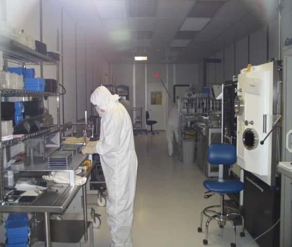
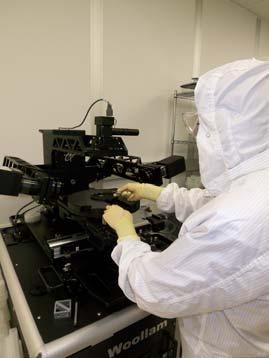
10 4. Sufficient Investment to take the business over the top Over $10 million invested by API Nanotronics Board in people, infrastructure and IP protection Waveplates High performance Filters Over 30 patents, 18 granted 36,000 sq. ft. State-of-the-art production facility with over 20,000 sq. ft. of clean-room and laboratory space Unique technical capabilities: Batch Atomic Layer Deposition (ALD) manufacturing tools Optical Isolators 10

11 5. A provable and sizable addressable market $7.3B * pure nanotechnology market 11

12 Some promising Nano Photonic developments that have the wholesome scent of application to them 1. Plasmonics 2. Metamaterials


13 1.Plasmonics Light-induced collective electronic excitations that can concentrate optical fields resulting for enhanced spectroscopic effects and can couple their energy out as photons for apparent light transmission through metal nanowires (ii) Plasmonic nanotags (i) Plasmonic conductance of light J. A. Hutchison, S. P. Centeno, H. Odaka, H. Fukumura, J. Hofkens, and H. Uji-i Nano Lett, 2009 G. B. Braun, S. J. Lee, T. Laurence, N. Fera, L. Fabris, G. C. Bazan, M. Moskovits, N. O. Reich, J. Phys. Chem. 2009

 Sub-wavelength")

14 Science, 2007 Negative refraction (may be used to make cloaking devices) Sub-wavelength resolution (UV-like lithography using visible light)

15


16 Silicon photonic crystals Geoff Ozin, Sajeev John, U of T Dream of an all-photonic computer Photonic crystal made by glancing angle deposition. Mike Brett, NINT
17 Conclusions Nano is ready for business as a tech tool but should not be an end in itself Combining nano with photons is a powerful combination. Combining nano with bio and photons is an even more powerful combination
Nanotechnology, the infrastructure, and IBM s research projects
 Nanotechnology, the infrastructure, and IBM s research projects Dr. Paul Seidler Coordinator Nanotechnology Center, IBM Research - Zurich Nanotechnology is the understanding and control of matter at dimensions
DTU DANCHIP an open access micro/nanofabrication facility bridging academic research and small scale production
 DTU DANCHIP an open access micro/nanofabrication facility bridging academic research and small scale production DTU Danchip National Center for Micro- and Nanofabrication DTU Danchip DTU Danchip is Denmark
Ultralight Weight Optical Systems using Nano-Layered Synthesized Materials
 Ultralight Weight Optical Systems using Nano-Layered Synthesized Materials Natalie Clark, PhD NASA Langley Research Center and James Breckinridge University of Arizona, College of Optical Sciences Overview
Georgia Tech IEN EBL Facility NNIN Highlights 2014 External User Projects
 Georgia Tech IEN EBL Facility NNIN Highlights 2014 External User Projects Silicon based Photonic Crystal Devices Silicon based photonic crystal devices are ultra-small photonic devices that can confine
REPORT DOCUMENTATION PAGE
 REPORT DOCUMENTATION PAGE Form Approved OMB No. 0704-0188 Public reporting burden for this collection of information is estimated to average 1 hour per response, including the time for reviewing instructions,
Energy beam processing and the drive for ultra precision manufacturing
 Energy beam processing and the drive for ultra precision manufacturing An Exploration of Future Manufacturing Technologies in Response to the Increasing Demands and Complexity of Next Generation Smart
Introduction Fundamentals of laser Types of lasers Semiconductor lasers
 ECE 5368 Introduction Fundamentals of laser Types of lasers Semiconductor lasers Introduction Fundamentals of laser Types of lasers Semiconductor lasers How many types of lasers? Many many depending on
Integrated electro-optical waveguide based devices with liquid crystals on a silicon backplane
 Integrated electro-optical waveguide based devices with liquid crystals on a silicon backplane Florenta Costache Group manager Smart Micro-Optics SMO/AMS Fraunhofer Institute for Photonic Microsystems,
Annual Report. University Of Alberta. Student Chapter
 Annual Report University Of Alberta Student Chapter 2009-2010 Student Chapter Member Roster Total Student Members : 25 Siamak Abdollahi 11 January 2011 Aassem Askari 31 October 2010 Mustafa Babadagli 20
FRAUNHOFER INSTITUTE FOR PHOTONIC MICROSYSTEMS IPMS. Application Area. Quality of Life
 FRAUNHOFER INSTITUTE FOR PHOTONIC MICROSYSTEMS IPMS Application Area Quality of Life Overlay image of visible spectral range (VIS) and thermal infrared range (LWIR). Quality of Life With extensive experience
SUPPLEMENTARY INFORMATION
 Optically reconfigurable metasurfaces and photonic devices based on phase change materials S1: Schematic diagram of the experimental setup. A Ti-Sapphire femtosecond laser (Coherent Chameleon Vision S)
Simulation of High Resistivity (CMOS) Pixels
 Pixels") Simulation of High Resistivity (CMOS) Pixels Stefan Lauxtermann, Kadri Vural Sensor Creations Inc. AIDA-2020 CMOS Simulation Workshop May 13 th 2016 OUTLINE 1. Definition of High Resistivity Pixel Also
Simulation of High Resistivity (CMOS) Pixels Stefan Lauxtermann, Kadri Vural Sensor Creations Inc. AIDA-2020 CMOS Simulation Workshop May 13 th 2016 OUTLINE 1. Definition of High Resistivity Pixel Also
Corporate Introduction of CRESTEC CORPORATION Expert in E-Beam Nanofabrication
 Corporate Introduction of CRESTEC CORPORATION Expert in E-Beam Nanofabrication David López-Romero Moraleda. Technical Support Manager, Crestec Corporation Spain Branch. Financiación-Internacionalización-Cooperación.
CHAPTER 2 POLARIZATION SPLITTER- ROTATOR BASED ON A DOUBLE- ETCHED DIRECTIONAL COUPLER
 CHAPTER 2 POLARIZATION SPLITTER- ROTATOR BASED ON A DOUBLE- ETCHED DIRECTIONAL COUPLER As we discussed in chapter 1, silicon photonics has received much attention in the last decade. The main reason is
Chemistry 524--"Hour Exam"--Keiderling Mar. 19, pm SES
 Chemistry 524--"Hour Exam"--Keiderling Mar. 19, 2013 -- 2-4 pm -- 170 SES Please answer all questions in the answer book provided. Calculators, rulers, pens and pencils permitted. No open books allowed.
Polarization Gratings for Non-mechanical Beam Steering Applications
 Polarization Gratings for Non-mechanical Beam Steering Applications Boulder Nonlinear Systems, Inc. 450 Courtney Way Lafayette, CO 80026 USA 303-604-0077 sales@bnonlinear.com www.bnonlinear.com Polarization
1.1 PHILOSOPHY OF MICRO/NANOFABRICATION
 CHAPTER Introduction 1 C H A P T E R C O N T E N T S 1.1 Philosophy of Micro/Nanofabrication... 1 1.2 The Industry Science Dualism... 5 1.3 Industrial Applications... 8 1.4 Purpose and Organization of
Spectral and Polarization Configuration Guide for MS Series 3-CCD Cameras
 Spectral and Polarization Configuration Guide for MS Series 3-CCD Cameras Geospatial Systems, Inc (GSI) MS 3100/4100 Series 3-CCD cameras utilize a color-separating prism to split broadband light entering
A process for, and optical performance of, a low cost Wire Grid Polarizer
 1.0 Introduction A process for, and optical performance of, a low cost Wire Grid Polarizer M.P.C.Watts, M. Little, E. Egan, A. Hochbaum, Chad Jones, S. Stephansen Agoura Technology Low angle shadowed deposition
MEDIA RELEASE FOR IMMEDIATE RELEASE 26 JULY 2016
 MEDIA RELEASE FOR IMMEDIATE RELEASE 26 JULY 2016 A*STAR S IME KICKS OFF CONSORTIA TO DEVELOP ADVANCED PACKAGING SOLUTIONS FOR NEXT-GENERATION INTERNET OF THINGS APPLICATIONS AND HIGH-PERFORMANCE WIRELESS
Highly efficient SERS nanowire/ag composites
 Highly efficient SERS nanowire/ag composites S.M. Prokes, O.J. Glembocki and R.W. Rendell Electronics Science and Technology Division Introduction: Optically based sensing provides advantages over electronic
NCN vision NCN vision 2002
 NCN: Global Initiative About "Electronics from the Bottom-up Director Network for Computational Nanotechnology gekco@purdue.edu NCN vision 2002 accelerate the transformation of nanoscience to nanotechnology
Supporting Information
 Electronic Supplementary Material (ESI) for Materials Horizons. This journal is The Royal Society of Chemistry 2017 Supporting Information Nanofocusing of circularly polarized Bessel-type plasmon polaritons
IMAGING SILICON NANOWIRES
 Project report IMAGING SILICON NANOWIRES PHY564 Submitted by: 1 Abstract: Silicon nanowires can be easily integrated with conventional electronics. Silicon nanowires can be prepared with single-crystal
Introduction of ADVANTEST EB Lithography System
 Introduction of ADVANTEST EB Lithography System Nanotechnology Business Division ADVANTEST Corporation 1 2 Node [nm] EB Lithography Products < ADVANTEST s Superiority > High Resolution :EB optical technology
Optical Waveguide Types
 8 Refractive Micro Optics Optical Waveguide Types There are two main types of optical waveguide structures: the step index and the graded index. In a step-index waveguide, the interface between the core
Deformable MEMS Micromirror Array for Wavelength and Angle Insensitive Retro-Reflecting Modulators Trevor K. Chan & Joseph E. Ford
 Photonics Systems Integration Lab UCSD Jacobs School of Engineering Deformable MEMS Micromirror Array for Wavelength and Angle Insensitive Retro-Reflecting Modulators Trevor K. Chan & Joseph E. Ford PHOTONIC
Noel Technologies. Provider of Advanced Lithography and Semiconductor Thin Film Services
 Noel Technologies Provider of Advanced Lithography and Semiconductor Thin Film Services Noel Technologies Keith Best Biography Over the last 27 years, Keith Best has held a variety of semiconductor processing
Electronically tunable fabry-perot interferometers with double liquid crystal layers
 Electronically tunable fabry-perot interferometers with double liquid crystal layers Kuen-Cherng Lin *a, Kun-Yi Lee b, Cheng-Chih Lai c, Chin-Yu Chang c, and Sheng-Hsien Wong c a Dept. of Computer and
A Presentation to the National Academies July 29, Larry W. Sumney President/CEO Semiconductor Research Corporation1
 A Presentation to the National Academies July 29, 2009 Larry W. Sumney President/CEO Semiconductor Research Corporation1 What is SRC? World s leading consortium funding collaborative university research
Design and fabrication of indium phosphide air-bridge waveguides with MEMS functionality
 Design and fabrication of indium phosphide air-bridge waveguides with MEMS functionality Wing H. Ng* a, Nina Podoliak b, Peter Horak b, Jiang Wu a, Huiyun Liu a, William J. Stewart b, and Anthony J. Kenyon
Prof. Matteo Rinaldi
 MATTEO RINALDI Prof. Matteo Rinaldi Northeastern SMART Vision and Mission Northeastern SMART Vision Conceive and pilot disruptive technological innovation in smart devices and systems to make everyday
MoS 2 nanosheet phototransistors with thicknessmodulated
 Supporting Information MoS 2 nanosheet phototransistors with thicknessmodulated optical energy gap Hee Sung Lee, Sung-Wook Min, Youn-Gyung Chang, Park Min Kyu, Taewook Nam, # Hyungjun Kim, # Jae Hoon Kim,
Introduction. Internet of things. Smart New World
 1 Introduction Internet of things Smart New World Source : iamwire IoT has evolved multiple technologies including sensors, embedded systems, communication, real-time analytics or machine learning. For
A new picosecond Laser pulse generation method.
 PULSE GATING : A new picosecond Laser pulse generation method. Picosecond lasers can be found in many fields of applications from research to industry. These lasers are very common in bio-photonics, non-linear
Silicon Photonics: A Platform for Integration, Wafer Level Assembly and Packaging
 Silicon Photonics: A Platform for Integration, Wafer Level Assembly and Packaging M. Asghari Kotura Inc April 27 Contents: Who is Kotura Choice of waveguide technology Challenges and merits of Si photonics
CHAPTER 7. Components of Optical Instruments
 CHAPTER 7 Components of Optical Instruments From: Principles of Instrumental Analysis, 6 th Edition, Holler, Skoog and Crouch. CMY 383 Dr Tim Laurens NB Optical in this case refers not only to the visible
INNOVATIVE SPECTRAL IMAGING
 INNOVATIVE SPECTRAL IMAGING food inspection precision agriculture remote sensing defense & reconnaissance advanced machine vision product overview INNOVATIVE SPECTRAL IMAGING Innovative diffractive optics
Industry Outlook September 2015
 Industry Outlook September 2015 Manufacturing Matters in Canada A $620 billion industry 12% of GDP (18% in 2004) 1.7 million direct employees (2.2 million in 2004) The largest payroll of any business sector
National Science Foundation Center for Lasers and Plasmas for Advanced Manufacturing. Mool C. Gupta Applied Research Center Old Dominion University
 National Science Foundation Center for Lasers and Plasmas for Advanced Manufacturing Mool C. Gupta Applied Research Center Old Dominion University National Science Foundation Center - Center Mission -
Winter College on Optics: Fundamentals of Photonics - Theory, Devices and Applications February 2014
 2572-10 Winter College on Optics: Fundamentals of Photonics - Theory, Devices and Applications 10-21 February 2014 Photonic packaging and integration technologies II Sonia M. García Blanco University of
NanoFabrication Kingston. Seminar and Webinar January 31, 2017 Rob Knobel Associate Professor, Dept. of Physics Queen s University
 NanoFabrication Kingston Seminar and Webinar January 31, 2017 Rob Knobel Associate Professor, Dept. of Physics Queen s University What is NFK? It s a place, an team of experts and a service. The goal of
Photonic Crystal Slot Waveguide Spectrometer for Detection of Methane
 Photonic Crystal Slot Waveguide Spectrometer for Detection of Methane Swapnajit Chakravarty 1, Wei-Cheng Lai 2, Xiaolong (Alan) Wang 1, Che-Yun Lin 2, Ray T. Chen 1,2 1 Omega Optics, 10306 Sausalito Drive,
On-chip interrogation of a silicon-on-insulator microring resonator based ethanol vapor sensor with an arrayed waveguide grating (AWG) spectrometer
 spectrometer") On-chip interrogation of a silicon-on-insulator microring resonator based ethanol vapor sensor with an arrayed waveguide grating (AWG) spectrometer Nebiyu A. Yebo* a, Wim Bogaerts, Zeger Hens b,roel Baets
On-chip interrogation of a silicon-on-insulator microring resonator based ethanol vapor sensor with an arrayed waveguide grating (AWG) spectrometer Nebiyu A. Yebo* a, Wim Bogaerts, Zeger Hens b,roel Baets
Characterising the Dynamics of Nano S&T: Implications for Future Policy
 MIoIR Characterising the Dynamics of Nano S&T: Implications for Future Policy A. Delemarle (U. Paris Est) With P. Larédo (Université Paris-Est - U. of Manchester) and B.Kahane (U. Paris Est) FRENCH- RUSSIAN
Societal Implications of Additive Manufacturing
 Societal Implications of Additive Manufacturing Additive Manufacturing for Government Conference Thomas A. Campbell, Ph.D. Research Associate Professor ICTAS Associate Director for Outreach Economic Environmental
More specifically, I would like to talk about Gallium Nitride and related wide bandgap compound semiconductors.
 Good morning everyone, I am Edgar Martinez, Program Manager for the Microsystems Technology Office. Today, it is my pleasure to dedicate the next few minutes talking to you about transformations in future
FEM simulations of nanocavities for plasmon lasers
 FEM simulations of nanocavities for plasmon lasers S.Burger, L.Zschiedrich, J.Pomplun, F.Schmidt Zuse Institute Berlin JCMwave GmbH 6th Workshop on Numerical Methods for Optical Nano Structures ETH Zürich,
Ultrafast Beams and Applications UBA July, 2017 Presenter: Arsham Yeremyan
 Laser driven facility for irradiation experiments, two-photon microscopy and microfabrication Ultrafast Beams and Applications UBA17 04-07 July, 2017 Presenter: Arsham Yeremyan Outline Parallel operation
New Optics for Astronomical Polarimetry
 New Optics for Astronomical Polarimetry Located in Colorado USA Topics Components for polarization control and polarimetry Organic materials Liquid crystals Birefringent polymers Microstructures Metrology
Continuum White Light Generation. WhiteLase: High Power Ultrabroadband
 Continuum White Light Generation WhiteLase: High Power Ultrabroadband Light Sources Technology Ultrafast Pulses + Fiber Laser + Non-linear PCF = Spectral broadening from 400nm to 2500nm Ultrafast Fiber
Fiberoptic and Waveguide Sensors
 Fiberoptic and Waveguide Sensors Wei-Chih Wang Department of Mecahnical Engineering University of Washington Optical sensors Advantages: -immune from electromagnetic field interference (EMI) - extreme
Adaptive multi/demultiplexers for optical signals with arbitrary wavelength spacing.
 Edith Cowan University Research Online ECU Publications Pre. 2011 2010 Adaptive multi/demultiplexers for optical signals with arbitrary wavelength spacing. Feng Xiao Edith Cowan University Kamal Alameh
Fiber-Optic Polarizer Using Resonant Tunneling through a Multilayer Overlay
 Fiber-Optic Polarizer Using Resonant Tunneling through a Multilayer Overlay Arun Kumar, Rajeev Jindal, and R. K. Varshney Department of Physics, Indian Institute of Technology, New Delhi 110 016 India
Des MEMS aux NEMS : évolution des technologies et des concepts aux travers des développements menés au LETI
 Des MEMS aux NEMS : évolution des technologies et des concepts aux travers des développements menés au LETI Ph. Robert 1 Content LETI at a glance From MEMS to NEMS: 30 years of technological evolution
Micro-sensors - what happens when you make "classical" devices "small": MEMS devices and integrated bolometric IR detectors
 Micro-sensors - what happens when you make "classical" devices "small": MEMS devices and integrated bolometric IR detectors Dean P. Neikirk 1 MURI bio-ir sensors kick-off 6/16/98 Where are the targets
LETI S SOLUTIONS FOR TERAHERTZ REAL-TIME IMAGING. Leti Photonics Workshop Simoens François February 1st, 2017
 LETI S SOLUTIONS FOR TERAHERTZ REAL-TIME IMAGING OUTLINE What & why Terahertz? THz imaging technologies developed at Leti Examples of real-time imaging applications Leti s offer to industrials Conclusion
End-of-line Standard Substrates For the Characterization of organic
 FRAUNHOFER INSTITUTe FoR Photonic Microsystems IPMS End-of-line Standard Substrates For the Characterization of organic semiconductor Materials Over the last few years, organic electronics have become
Absentee layer. A layer of dielectric material, transparent in the transmission region of
 Glossary of Terms A Absentee layer. A layer of dielectric material, transparent in the transmission region of the filter, due to a phase thickness of 180. Absorption curve, absorption spectrum. The relative
CORPORATE PRESENTATION
 CORPORATE PRESENTATION WHO WE ARE Edmund Optics is a global OPTICS and IMAGING company that manufactures and supplies the worldwide technical community with precision optical components and subassemblies.
Discovering Electrical & Computer Engineering. Carmen S. Menoni Professor Week 3 armain.
 Discovering Electrical & Computer Engineering Carmen S. Menoni Professor Week 3 http://www.engr.colostate.edu/ece103/semin armain.html TOP TECH 2012 SPECIAL REPORT IEEE SPECTRUM PAGE 28, JANUARY 2012 P.E.
A novel tunable diode laser using volume holographic gratings
 A novel tunable diode laser using volume holographic gratings Christophe Moser *, Lawrence Ho and Frank Havermeyer Ondax, Inc. 85 E. Duarte Road, Monrovia, CA 9116, USA ABSTRACT We have developed a self-aligned
A Brief Introduction to Single Electron Transistors. December 18, 2011
 A Brief Introduction to Single Electron Transistors Diogo AGUIAM OBRECZÁN Vince December 18, 2011 1 Abstract Transistor integration has come a long way since Moore s Law was first mentioned and current
Micro-PackS, Technology Platform. Security Characterization Lab Opening
 September, 30 th 2008 Micro-PackS, Technology Platform Security Characterization Lab Opening Members : Micro-PackS in SCS cluster From Silicium to innovative & commucating device R&D structure, gathering
Section 2: Lithography. Jaeger Chapter 2 Litho Reader. The lithographic process
 Section 2: Lithography Jaeger Chapter 2 Litho Reader The lithographic process Photolithographic Process (a) (b) (c) (d) (e) (f) (g) Substrate covered with silicon dioxide barrier layer Positive photoresist
Advances in Laser Micro-machining for Wafer Probing and Trimming
 Advances in Laser Micro-machining for Wafer Probing and Trimming M.R.H. Knowles, A.I.Bell, G. Rutterford & A. Webb Oxford Lasers June 10, 2002 Oxford Lasers June 2002 1 Introduction to Laser Micro-machining
Partnering along the chain of innovation : III-V lab example
 Partnering along the chain of innovation : III-V lab example Dominique Pons Symposium Global Open Innovation Networks What is III-V Lab? a jointly owned Alcatel-Lucent / Thales R&D Lab French GIE (Groupement
Cooled cameras for scientific applications and astronomy. Ian Alderton Alrad Imaging division of Alrad Instruments Ltd
 Cooled cameras for scientific applications and astronomy Ian Alderton Alrad Imaging division of Alrad Instruments Ltd www.alrad.co.uk History 1970 - started as Wenzel Elektronic UK in NIM modules and radiation
Nanomanufacturing and Fabrication By Matthew Margolis
 Nanomanufacturing and Fabrication By Matthew Margolis Manufacturing is the transformation of raw materials into finished goods for sale, or intermediate processes involving the production or finishing
Georgia Electronic Commerce Association. Dr. G. Wayne Clough, President Georgia Institute of Technology April 30, 2003
 Georgia Electronic Commerce Association Dr. G. Wayne Clough, President Georgia Institute of Technology April 30, 2003 Georgia Tech: Driving high-end economic development Oak Ridge National Laboratory National
Waveguiding in PMMA photonic crystals
 ROMANIAN JOURNAL OF INFORMATION SCIENCE AND TECHNOLOGY Volume 12, Number 3, 2009, 308 316 Waveguiding in PMMA photonic crystals Daniela DRAGOMAN 1, Adrian DINESCU 2, Raluca MÜLLER2, Cristian KUSKO 2, Alex.
WHITE PAPER MINIATURIZED HYPERSPECTRAL CAMERA FOR THE INFRARED MOLECULAR FINGERPRINT REGION
 WHITE PAPER MINIATURIZED HYPERSPECTRAL CAMERA FOR THE INFRARED MOLECULAR FINGERPRINT REGION Denis Dufour, David Béland, Hélène Spisser, Loïc Le Noc, Francis Picard, Patrice Topart January 2018 Low-cost
Dual Vivaldi UWB nanoantenna for optical applications
 Dual Vivaldi UWB nanoantenna for optical applications Zeev Iluz, Yuval Yifat, Doron Bar-Lev, Michal Eitan, Yoni Kantarovsky, Yuav Blue, Yael Hanein, Koby Scheuer, and Amir Boag School of Electrical Engineering
Optimization of supercontinuum generation in photonic crystal fibers for pulse compression
 Optimization of supercontinuum generation in photonic crystal fibers for pulse compression Noah Chang Herbert Winful,Ted Norris Center for Ultrafast Optical Science University of Michigan What is Photonic
Canada s National Design Network. Community Research Innovation Opportunity
 Canada s National Design Network Community Research Innovation Opportunity Over the past five years, more than 7000 researchers in the National Design Network have benefited from industrial tools, technologies,
Thermal treatment method for tuning the lasing wavelength of a DFB fiber laser using coil heaters
 Thermal treatment method for tuning the lasing wavelength of a DFB fiber laser using coil heaters Ha Huy Thanh and Bui Trung Dzung National Center for Technology Progress (NACENTECH) C6-Thanh Xuan Bac-Hanoi-Vietnam
Section 2: Lithography. Jaeger Chapter 2 Litho Reader. EE143 Ali Javey Slide 5-1
 Section 2: Lithography Jaeger Chapter 2 Litho Reader EE143 Ali Javey Slide 5-1 The lithographic process EE143 Ali Javey Slide 5-2 Photolithographic Process (a) (b) (c) (d) (e) (f) (g) Substrate covered
Spotlight 150 and 200 FT-IR Microscopy Systems
 S P E C I F I C A T I O N S Spotlight 150 and 200 FT-IR Microscopy Systems FT-IR Microscopy Spotlight 200 with Frontier FT-IR Spectrometer Introduction PerkinElmer Spotlight FT-IR Microscopy Systems are
Bottom-up Nanostructures just a research hype?
 Fakultät Maschinenwesen, Institut für Werkstoffwissenschaft, Professur Materialwissenschaft u. Nanotechnik Bottom-up Nanostructures just a research hype? Dr.-Ing. Alexander Nerowski Dresden, 22.09.2017
IBM Research - Zurich Research Laboratory
 October 28, 2010 IBM Research - Zurich Research Laboratory Walter Riess Science & Technology Department IBM Research - Zurich wri@zurich.ibm.com Outline IBM Research IBM Research Zurich Science & Technology
Robert Magnusson, Ph.D.
 Robert Magnusson, Ph.D. Texas Instruments Distinguished University Chair in Nanoelectronics Director of the Nanophotonics Device Group Co-founder and Chief Technical Officer of Resonant Sensors Incorporated
Understanding Optical Specifications
 Understanding Optical Specifications Optics can be found virtually everywhere, from fiber optic couplings to machine vision imaging devices to cutting-edge biometric iris identification systems. Despite
NIR SPECTROSCOPY Instruments
 What is needed to construct a NIR instrument? NIR SPECTROSCOPY Instruments Umeå 2006-04-10 Bo Karlberg light source dispersive unit (monochromator) detector (Fibres) (bsorbance/reflectance-standard) The
Nanostencil Lithography and Nanoelectronic Applications
 Microsystems Laboratory Nanostencil Lithography and Nanoelectronic Applications Oscar Vazquez, Marc van den Boogaart, Dr. Lianne Doeswijk, Prof. Juergen Brugger, LMIS1 Dr. Chan Woo Park, Visiting Professor
Introduction to the operating principles of the HyperFine spectrometer
 Introduction to the operating principles of the HyperFine spectrometer LightMachinery Inc., 80 Colonnade Road North, Ottawa ON Canada A spectrometer is an optical instrument designed to split light into
CONFIGURING. Your Spectroscopy System For PEAK PERFORMANCE. A guide to selecting the best Spectrometers, Sources, and Detectors for your application
 CONFIGURING Your Spectroscopy System For PEAK PERFORMANCE A guide to selecting the best Spectrometers, s, and s for your application Spectral Measurement System Spectral Measurement System Spectrograph
SUPPLEMENTARY INFORMATION
 SUPPLEMENTARY INFORMATION DOI: 10.1038/NNANO.2015.137 Controlled steering of Cherenkov surface plasmon wakes with a one-dimensional metamaterial Patrice Genevet *, Daniel Wintz *, Antonio Ambrosio *, Alan
MULTI-CRYSTAL ACHROMATIC RETARDER FOR VISIBLE REGION APPLICATIONS
 MULTI-CRYSTAL ACHROMATIC RETARDER FOR VISIBLE REGION APPLICATIONS Nilanjan Mukhopadhyay 1 and Saswati De 2 1,2 Department of Electronics & Communication Engineering, Global Institute of Management and
CHARGE-COUPLED DEVICE (CCD)
") CHARGE-COUPLED DEVICE (CCD) Definition A charge-coupled device (CCD) is an analog shift register, enabling analog signals, usually light, manipulation - for example, conversion into a digital value that
CHARGE-COUPLED DEVICE (CCD) Definition A charge-coupled device (CCD) is an analog shift register, enabling analog signals, usually light, manipulation - for example, conversion into a digital value that
EUV and Soft X-Ray Optics
 David Attwood University of California, Berkeley Cheiron School September 2012 SPring-8 1 The short wavelength region of the electromagnetic spectrum n = 1 + i,
Electronic-Photonic ICs for Low Cost and Scalable Datacenter Solutions
 Electronic-Photonic ICs for Low Cost and Scalable Datacenter Solutions Christoph Theiss, Director Packaging Christoph.Theiss@sicoya.com 1 SEMICON Europe 2016, October 27 2016 Sicoya Overview Spin-off from
Development of Nano Second Pulsed Lasers Using Polarization Maintaining Fibers
 Development of Nano Second Pulsed Lasers Using Polarization Maintaining Fibers Shun-ichi Matsushita*, * 2, Taizo Miyato*, * 2, Hiroshi Hashimoto*, * 2, Eisuke Otani* 2, Tatsuji Uchino* 2, Akira Fujisaki*,
Laser Scanning for Surface Analysis of Transparent Samples - An Experimental Feasibility Study
 STR/03/044/PM Laser Scanning for Surface Analysis of Transparent Samples - An Experimental Feasibility Study E. Lea Abstract An experimental investigation of a surface analysis method has been carried
Scintillation Counters
 PHY311/312 Detectors for Nuclear and Particle Physics Dr. C.N. Booth Scintillation Counters Unlike many other particle detectors, which exploit the ionisation produced by the passage of a charged particle,
Performance of Microchannel Plates Fabricated Using Atomic Layer Deposition
 Performance of Microchannel Plates Fabricated Using Atomic Layer Deposition Andrey Elagin on behalf of the LAPPD collaboration Introduction Performance (timing) Conclusions Large Area Picosecond Photo
Project Staff: Timothy A. Savas, Michael E. Walsh, Thomas B. O'Reilly, Dr. Mark L. Schattenburg, and Professor Henry I. Smith
 9. Interference Lithography Sponsors: National Science Foundation, DMR-0210321; Dupont Agreement 12/10/99 Project Staff: Timothy A. Savas, Michael E. Walsh, Thomas B. O'Reilly, Dr. Mark L. Schattenburg,
MASSACHUSETTS INSTITUTE OF TECHNOLOGY Department of Electrical Engineering and Computer Science
 Student Name Date MASSACHUSETTS INSTITUTE OF TECHNOLOGY Department of Electrical Engineering and Computer Science 6.161 Modern Optics Project Laboratory Laboratory Exercise No. 6 Fall 2010 Solid-State
Controlling spatial modes in waveguided spontaneous parametric down conversion
 Controlling spatial modes in waveguided spontaneous parametric down conversion Michał Karpiński Konrad Banaszek, Czesław Radzewicz Faculty of Physics University of Warsaw Poland Ultrafast Phenomena Lab
The Development of a High Quality and a High Peak Power Pulsed Fiber Laser With a Flexible Tunability of the Pulse Width
 The Development of a High Quality and a High Peak Power Pulsed Fiber Laser With a Flexible Tunability of the Pulse Width Ryo Kawahara *1, Hiroshi Hashimoto *1, Jeffrey W. Nicholson *2, Eisuke Otani *1,