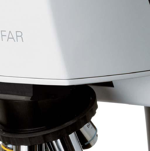
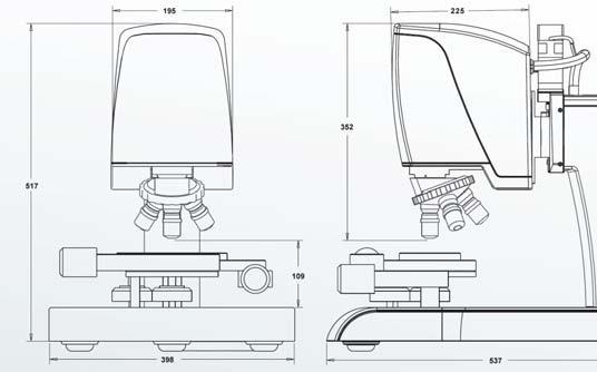
System Configuration 3D Optical Profi ler Dimensions SENSOFAR SENSOFAR-TECH, SL. TERRASSA SENSOFAR Japan Ltd.
|
|
|
- Aileen Hudson
- 6 years ago
- Views:
Transcription


1 3D Optical Profiler


 can be employed to measure large fields of view with the same height resolution. However, the measurement range is limited to a few micrometers by the coherence length.")


2 SENSOFAR TECHNOLOGY In recent years, interferometers and confocal imaging profilers have been competing in the non-contact surface metrology market. Both devices can accurately and reliably measure surface topographies on the scale of millimeters to sub-nanometers. Now, Sensofar has made a breakthrough in non-contact optical 3D profiling: the neox. This sensor head combines both confocal and interferometry techniques, as well as thick and thin film measurement capabilities. The combination of techniques makes the neox a unique system that outperforms all existing optical profilers. In addition to its compact and robust design, the neox is a complete tool that is ideal for obtaining a fast, non-invasive assessment of the micro- and nano-geometry of technical surfaces in multiple configurations: from the standard setup for R&D and quality inspection laboratories to sophisticated, customized solutions for online process controls. Interferometry In an interferometer, a light beam passes through a beam splitter, which directs the light to both the surface of the sample and a built-in reference mirror. The light reflected from these surfaces recombines and a fringe interference pattern is formed. PSI profiling Phase shift interferometers have been developed to measure the surface height of very smooth and continuous surfaces with sub-nanometer resolution. The sample, which must be in focus, is scanned vertically in a few steps that are a very precise fraction of the wavelength. The profiling algorithms produce a phase map of the surface, which is converted to the corresponding height map by means of a suitable unwrapping procedure. PSI profiling provides sub-nanometer vertical resolution for all numerical apertures (NA). Very low magnifications (2.5X) can be employed to measure large fields of view with the same height resolution. However, the measurement range is limited to a few micrometers by the coherence length. PSI algorithms enable the neox to profile shape features on the nanometer scale, and to assess texture parameters of super smooth surfaces on the sub-nanometer scale. VSI profiling White-light vertical scanning interferometers ters have been developed to measure the surface height of smooth to moderately rough surfaces. Maximum fringe contrast occurs at the best focus position for each point on the surface of the sample. The sample is scanned vertically in steps so that every point on the surface passes through the focus. The height of the surface at each pixel location is found by detecting the peak of the narrow fringe envelopes. Confocal profiling VSI profiling provides nanometer vertical resolution for all NA. The VSI algorithms enable the neox to use all the available magnifications to profile shape features with the same height resolution. The measurement range is intrinsically unlimited, although in practice it is limited to the working distance of the objective. Scan speeds and data acquisition rates can be very fast, although this leads to a significant loss of vertical resolution. Confocal profilers have been developed to measure the surface height of smooth to very rough surfaces. A confocal imaging system provides high contrast images by eliminating out-of-focus light. The sample is scanned vertically in steps so that every point on the surface passes through the focus. The height of the surface at each pixel location is found by detecting the peak of the narrow axial response. As only local areas of the surface are illuminated simultaneously, in-plane raster scanning is required to build up the axial response (i.e. the confocal image) at each vertical step. Confocal profiling provides the highest lateral l resolution that can be achieved by an optical profiler. Thus, spatial sampling can be reduced to 0.10 μm, which is ideal for critical cal dimension ion measurements. High NA (0.95) and magnification io (150X and 200X) objectives are available to measure smooth surfaces with steep local slopes (over 70º). The neox has extremely high light efficiency and an unlimited intrinsic measurement range. The proprietary r confocal algorithms provide vertical repeatability abi on the nanometer scale. Super-long working distance (SLWD) objectives are available to measure high aspect ratio features, large steps and steeply sloping samples. Step height measurements can also be made in structured or stratified samples that contain dissimilar materials. Thin Film Spectroscopic reflectometry is one of the preferred methods for measuring thin films because it is accurate, nondestructive, very fast and requires no sample preparation. In spectroscopic reflectometry, the surface is illuminated with white light. Light is reflected at the different interfaces of the thin film structure. All reflections are superposed coherently and interferential effects occur. As a result, the intensity of the reflected light shows variations in wavelength that depend on the thickness and refractive index of the different layers of the thin film structure. Software compares the real measured spectrum with a simulated one and optimizes the thicknesses of the thin films until the best fit is attained. The neox can also be used as a high lateral resolution thin film measurement system. It works very well for single foils, membranes or single thin layers on a substrate, and it can also deal with more sophisticated structures (up to ten layers on a substrate). Transparent films from 10 nm to 20 μm can be measured in less than one second with a thickness resolution of 0.1 nm and a lateral resolution up to 5 μm.


3 MARKETS & APPLICATIONS The PLu Series plays a key role in demanding industries such as the semiconductor, biomedical, and biotechnology ology industries. Sensofar optical profilers are installed in many R&D facilities and quality control departments for micro-, nano- and sub-nano applications to analyze the 3D surface characterization cterization of the material. Applications ENERGY. Thin film, silicon solar cells, power cells, ceramics. BIOMEDICAL. Microfluidics, passivation, drug and hygiene coatings, catheter, balloon, stents. OPTICS. Transmission, roughness, anti-fog, hardness coatings, profile of aspherics. CCD Bayer matrix FLAT PANEL DISPLAY. RGB cells, photospacers, coatings, defect analysis. Fluidodinamycs channels MATERIALS. Roughness, tribology, hardness test, fatigue. LCD, RGB Filter Four different solar cells LED. Emission substrate. IC PACKAGING. Flip Chip. Steel LED structures SEMICONDUCTOR. Photoresists for masks, thickness, of Si thin membranes, insulation, MEMs. MEM s Flip Chip. Zoom on a stanium ball


4 INSTRUMENT The neox is an optical profiler that has been developed by Sensofar using propietary technology. The extremely high light efficiency of the illumination hardware and the high contrast algorithms are the main advantages of Sensofar s confocal arrangement. These features make the system ideal for measuring steep slopes, rough and reflective surfaces and samples containing dissimilar materials. The high quality interferometry optics and the integrated piezo scanner are the key elements to interferometric profiling. This technology is ideal for measuring very smooth to moderately rough surfaces. The combination of these techniques provides an endless range of applications. The neox can be used for standard bright-field color microscopy imaging, confocal imaging, 3D confocal profiling, PSI, VSI and highresolution thin film thickness measurements. The robust and compact design, which is based on microdisplay technology and has no moving parts, also makes this sensor head suitable for OEM applications. The extremely simple and ergonomic software interface enables the user to obtain the measurement very fast, by simply choosing the right objective and focusing and selecting the appropriate acquisition technique.


5 SYSTEM PERFORMANCE Microdisplay-based confocal scanning Integrated spectroscopic reflectometer Practical limits for confocal and interferential methods for film thickness measures are to the order of 1 μm, and limited to a single layer. The neox incorporates a spectroscopic reflectometer through an optical fiber for the measurement of thin films, with thicknesses ranging from 10 nm and up to 10 layer stacks. The optical fiber is imaged through the microscope s objectives. Thus, thin films can be measured with spots as small as 5 μm. The measurement is undertaken with the integrated LED light source, which provides real-time bright-field images of the sample and simultaneous thin-film measurements. Color CCD camera Existing confocal microscopes use mirror scanning heads, which are movable mechanisms that limit lifetime and degrade pixel dithering at high magnifications. For confocal scanning, the neox uses the Sensofar s patented technology, which is based on a microdisplay. The microdisplay is based on ferroelectric liquid crystal on silicon (FLCoS), a fast switching device with no moving parts that makes the scanning of confocal images fast and very stable with an unlimited lifetime. Diffraction-limited structures of 0.2 μm. Courtesy of Obducat technologies. Dual LED Two high-power LEDs are integrated into the light source. A white LED is used for color brightfield inspection, thin-film metrology, VSI and epsi, and a blue LED is used for high-resolution confocal imaging and PSI. The short wavelength of the blue LED increases the lateral resolution to 0.15 μm (L&S) and improves PSI noise to 0.01 nm of vertical resolution. An objective lens for each application The neox uses premium CFI60 Nikon objectives lenses, which have the largest working distance for each NA. Over 50 lenses are available. Each one suits a specific application: high NA is used for confocal imaging and profiling, with a magnification range of 2.5X to 200X, super-long working distance, extra-long working distance and water immersion objective lenses; collar ring adjustment for focusing through transparent media up to 2 mm thickness; and interferential objectives lenses of 2.5X to 100X magnification, with reference mirror correction and incorporated tip-tilt. The neox uses a black and white, high-speed, high-resolution CCD camera as the system s metrological detector. A color camera can be used for bright-field surface inspection. This makes it easy to identify the features of the sample under analysis. In addition, an infinite focused color image can be obtained from topography measurements. The system acquires color images during vertical scanning and assigns to each pixel the color of the image obtained at the z position where the surface was in focus. The infinite focused color image can be used to create impressive 3D views of the measurements. Dual vertical scanner The dual vertical scanner consists of a motorized stage and a piezo for the highest scanning range and the highest measurement accuracy and repeatability. The linear stage has a 40-mm travel range and high position accuracy. Steps as small as 10 nm can be made, which is ideal for confocal scanning. Other objective lenses for specific applications are also available. Please visit for more information. High speed (12.5 confocal fps) The fast switching speed of the FLCoS microdisplay and proprietary confocal algorithms lead to a confocal rate of 12.5 confocal images per second. Due to this high frame rate, vertical 3D scanning is performed at 8 planes/s, which means that the scanning speed for confocal 3D measurements ranges of 0.5 to 350 μm/s. Interferential scanning and profile measurements are performed at 50 fps, which means that the vertical scanning speed is up to 800 μm/s. A typical measurement time that includes calculations after the scan is less than 5 seconds. The integrated piezo scanner has a range of up to 200 μm, with piezo resistive sensors for high position resolution of 0.2 nm and 1 nm of accuracy cy on the full travel range. Existing scanning stages with an optical encoder have 30 nm of uncertainty, which limits system repeatability and accuracy. The neox, with its unique combination of a linear stage and a piezo scanner, has the highest accuracy, linearity and repeatability ity on the market, with a measurement range from 0.1 nm to several mm. 10 nm step height and dental implant Ink dots on stamp

 NA FOV (μm) 1 Spatial sampling (μm) 2 Optical Resolution (L&S) (μm) 3 Maximum Slope 4 Vertical Resolution (nm) 5 Confocal Frame rate (frame/s) Scanning speed (μm/s) Typical")

6 SOFTWARE SPECIFICATIONS SensoSCAN software provides an interface with which any measurement can easily be taken, as well as a basic set of tools for displaying and analyzing data. SensoSCAN uses OpenGL technology to provide complete 3D surface visibility at any angle. Automated measurements are obtained using the Recipes and Sequence tool. A fully automated process (measurement and analysis) can be undertaken in combination with two external software applications: SensoMAP or SensoPRO. Working Distance (mm) NA FOV (μm) 1 Spatial sampling (μm) 2 Optical Resolution (L&S) (μm) 3 Maximum Slope 4 Vertical Resolution (nm) 5 Confocal Frame rate (frame/s) Scanning speed (μm/s) Typical measurement time (s) 6 5X x º < X x º < Confocal objectives 20X x º <20 50X x º < fps X x º < X x º < Interferometry objectives SensoSCAN features: Brightfield/confocal image, topography, stitching and thickness measurements. Automated measurements using the Recipes and Sequence tool. Interactive 2D and 3D surface views. A basic set of display and analysis tools. Integration of standards for 2D parameters. SensoPRO features: Fully automated monitoring of the production process. Controls the external devices that handle the samples, such as wafer loaders or SCARA robots using the SECS protocol. Plug-in-based data analysis algorithms provide a high degree of flexibility. Current capabilities include BGA bump, VIA, copper traces, solder resistance and anchor critical dimension analysis for the IC packaging industry. New modules can be easily customized to other industry needs. SensoMAP, which is based on Mountains technology from Digital Surf, is state-of-the-art surface analysis software. R&D departments and production facilities use Mountains for 2D/3D surface characterization. SensoMAP is a suitable tool for monitoring and evaluating surface changes during the life cycle of a material or component. SensoMAP software is completely modular. Four different levels (basic, FFT, Plus and Turbo) and five modules (4F Series, Contour, Grains & Particles, Statistics and Stitching) are available. SensoMAP features: A full set of tools for carrying out advanced analysis, including different surface views and operators. An intuitive desktop environment. Fast data reporting. Automated analysis by applying the same analysis workflow to different measurement data sets. Integration of standards: ISO 25178, which is the first international standard on 3D areal surface texture, EUR EN and full support for 2D parameters. Advanced, multilingual environment that makes the software userfriendly. Six European languages, Japanese and Chinese are available. Working Distance (mm) NA FOV (μm) 1 Spatial sampling (μm) 2 Optical Resolution blue (L&S) (μm) 3 Optical Resolution white (L&S) (μm) 3 Maximum Slope 4 Vertical Resolution (nm) PSI 7 Vertical Resolution (nm) epsi 7 Vertical Resolution (nm) VSI 8 Vertical Range PSI (μm) Vertical Range epsi (μm) Vertical Range VSI (mm) Scanning speed (μm/s) Typical measurement time (s) 9 2.5X x º 1) Maximum field of view with ½ camera and 0.5X optics. 2) Pixel size on the surface 3) Half of the diffraction limit according to the Rayleight criterion. L&S: Line and Space. Blue wavelength 460 nm, and White central wavelength 550 nm. 4) On smooth surfaces 5) System noise measured as the difference between two consecutive measures with 2 confocal image averages on a calibration mirror placed perpendicular to the optical axis. 5X x º 10X x º 20X x º <0.1 nm (down to 0.01 nm with PZT) 1 nm 5 μm 100 μm 10 mm PSI: 3-15 μm/s VSI/ePSI: 4-18 μm/s PSI: 3 s VSI: 10s epsi: 30s 50X x º 100X x º 6) For 21 scanning planes. 7) System noise measured as the difference between two consecutive measures with 10 phase averages on a calibration mirror placed perpendicular to the optical axis. Vibration isolation activated. The 0.01 nm are achieved with Piezo stage scanner and temperature controlled room. 8) System noise measured as the difference between two consecutive measures on a calibration mirror placed to the perpendicular axis. Vibration isolation activated. 9) For 10 μm scan range Visit for additional information. Other Specifications Measurement Array: 576 x 768 Bright Field Frame Rate: 50 fps Other Objectives Are Available. Confocal: Water immersion, Super Long Working Distance, Extra Long Working Distance, Collar Ring depth focusing correction Interferometry: Variable reflectance, Michelson, Mirau and Linnik Sample Size: from 40 mm to 500 mm. Larger under request Sample Reflectivity: from 0.1% to 100% Display Resolution: 0.01 nm Vertical Scanning Range: 40 mm with Linear Stage. Up to 200 μm with Piezo stage Linearity: better than 0.05%. <0.5 μm/mm with Linear Stage, and <50 nm/100 μm with PZT Step Height Repeatability: 0.1% Roughness Repeatability: <0.2% Step Height Accuracy: 0.5% Environment Temperature: 5ºC to 40ºC Humidity: <80% RH Altitude: <2000 m Power Requirements Input Voltage: 110/220Vac, single phase 50/60Hz
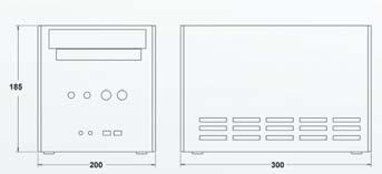
7 System Configuration Dimensions (unit: mm) Computer Control electronics SENSOFAR is a leading-edge technology company operating at the highest quality standards within the field of non-contact surface metrology. We provide highaccuracy optical profilers based on interferometry and confocal techniques. From standard setups for R&D and quality inspection laboratories, to complete non contact metrology solutions for online production processes, Sensofar is offering a technology enabling our customers to achieve the most challenging breakthroughs, particularly in semiconductor, precision optics, data storage, display devices, thick and thin films and material testing technologies, in more than 15 countries through Channel Partners and with own office in Japan. Headquarters and sales office SENSOFAR-TECH, SL. IPCT - Mòdul TR20 Ctra. N 150, km 14, TERRASSA (SPAIN) Tel. (+34) Fax (+34) info@sensofar.com - Sales office SENSOFAR Japan Ltd. Ichikawa Business Plaza 405, Minami-Yawata ICHIKAWA-SHI, CHIBA, (JAPAN) Tel. (+81) Fax (+81) info@sensofar.co.jp -
Non-contact 3D optical profiler
 Non-contact 3D optical profiler Sensofar s S line Feel the 3 The new S line for non-contact optical 3D profiling. The line that opens the way to a new 3D experience. Designed as a high-performance 3D optical
SUPRA Optix 3D Optical Profiler
 SUPRA Optix 3D Optical Profiler Scanning White-light Interferometric Microscope SWIM Series Applications The SUPRA Optix is the latest development in the field of Scanning White-light Interferometry. With
Advanced 3D Optical Profiler using Grasshopper3 USB3 Vision camera
 Advanced 3D Optical Profiler using Grasshopper3 USB3 Vision camera Figure 1. The Zeta-20 uses the Grasshopper3 and produces true color 3D optical images with multi mode optics technology 3D optical profiling
Measurement of Surface Profile and Layer Cross-section with Wide Field of View and High Precision
 Hitachi Review Vol. 65 (2016), No. 7 243 Featured Articles Measurement of Surface Profile and Layer Cross-section with Wide Field of View and High Precision VS1000 Series Coherence Scanning Interferometer
Bringing Answers to the Surface
 3D Bringing Answers to the Surface 1 Expanding the Boundaries of Laser Microscopy Measurements and images you can count on. Every time. LEXT OLS4100 Widely used in quality control, research, and development
Zeta-20. Zeta3D OPTICAL PROFILER IMAGING THE IMPOSSIBLE
 Zeta3D OPTICAL PROFILER Zeta-20 IMAGING THE IMPOSSIBLE TRUE COLOR 3D DIC BRIGHT FIELD DARK FIELD POLARIZED LIGHT IMAGE THROUGH TRANSMISSIVE IMAGE WHITE OR BLUE LED LIGHT SOURCE THIN FILM THICKNESS DIAMOND
Zeta-300 3D OPTICAL PROFILER
 Zeta-300 3D OPTICAL PROFILER Technology Toolkit Developed in 2007, the revolutionary Confocal Grid Structured Illumination (CGSI) is the powerful technology in all Zeta Optical Profilers but in a Zeta,
Super High Vertical Resolution Non-Contact 3D Surface Profiler BW-S500/BW-D500 Series
 Super High Vertical Resolution Non-Contact 3D Surface Profiler BW-S500/BW-D500 Series Nikon's proprietary scanning-type optical interference measurement technology achieves 1pm* height resolution. * Height
ASM Webinar Digital Microscopy for Materials Science
 Digital Microscopy Defined The term Digital Microscopy applies to any optical platform that integrates a digital camera and software to acquire images; macroscopes, stereomicroscopes, compound microscopes
Optical Characterization and Defect Inspection for 3D Stacked IC Technology
 Minapad 2014, May 21 22th, Grenoble; France Optical Characterization and Defect Inspection for 3D Stacked IC Technology J.Ph.Piel, G.Fresquet, S.Perrot, Y.Randle, D.Lebellego, S.Petitgrand, G.Ribette FOGALE
Manufacturing Metrology Team
 The Team has a range of state-of-the-art equipment for the measurement of surface texture and form. We are happy to discuss potential measurement issues and collaborative research Manufacturing Metrology
High-Speed 3D Sensor with Micrometer Resolution Ready for the Production Floor
 High-Speed 3D Sensor with Micrometer Resolution Ready for the Production Floor Industrial VISION days 2011 10.11.2011 Christian Lotto acquisiton Speed, vibration tolerance Challenge: High Precision on
Difrotec Product & Services. Ultra high accuracy interferometry & custom optical solutions
 Difrotec Product & Services Ultra high accuracy interferometry & custom optical solutions Content 1. Overview 2. Interferometer D7 3. Benefits 4. Measurements 5. Specifications 6. Applications 7. Cases
attocfm I for Surface Quality Inspection NANOSCOPY APPLICATION NOTE M01 RELATED PRODUCTS G
 APPLICATION NOTE M01 attocfm I for Surface Quality Inspection Confocal microscopes work by scanning a tiny light spot on a sample and by measuring the scattered light in the illuminated volume. First,
Systematic Workflow via Intuitive GUI. Easy operation accomplishes your goals faster than ever.
 Systematic Workflow via Intuitive GUI Easy operation accomplishes your goals faster than ever. 16 With the LEXT OLS4100, observation or measurement begins immediately once the sample is placed on the stage.
nanovea.com PROFILOMETERS 3D Non Contact Metrology
 PROFILOMETERS 3D Non Contact Metrology nanovea.com PROFILOMETER INTRO Nanovea 3D Non-Contact Profilometers are designed with leading edge optical pens using superior white light axial chromatism. Nano
Application Note #548 AcuityXR Technology Significantly Enhances Lateral Resolution of White-Light Optical Profilers
 Application Note #548 AcuityXR Technology Significantly Enhances Lateral Resolution of White-Light Optical Profilers ContourGT with AcuityXR TM capability White light interferometry is firmly established
attosnom I: Topography and Force Images NANOSCOPY APPLICATION NOTE M06 RELATED PRODUCTS G
 APPLICATION NOTE M06 attosnom I: Topography and Force Images Scanning near-field optical microscopy is the outstanding technique to simultaneously measure the topography and the optical contrast of a sample.
Coherence radar - new modifications of white-light interferometry for large object shape acquisition
 Coherence radar - new modifications of white-light interferometry for large object shape acquisition G. Ammon, P. Andretzky, S. Blossey, G. Bohn, P.Ettl, H. P. Habermeier, B. Harand, G. Häusler Chair for
Dynamic Phase-Shifting Microscopy Tracks Living Cells
 from photonics.com: 04/01/2012 http://www.photonics.com/article.aspx?aid=50654 Dynamic Phase-Shifting Microscopy Tracks Living Cells Dr. Katherine Creath, Goldie Goldstein and Mike Zecchino, 4D Technology
Confocal NEXIV VMZ-K Series. CNC Video Measuring System CONFOCAL NEXIV. VMZ-K Series
 Confocal NEXIV VMZ-K Series CNC Video Measuring System CONFOCAL NEXIV VMZ-K Series 3D FOV Measurements Generated with Confocal Images The Confocal NEXIV VMZ-K series, a ground-breaking multifunctional
Confocal NEXIV VMZ-K Series. CNC Video Measuring System CONFOCAL NEXIV. VMZ-K Series
 Confocal NEXIV VMZ-K Series CNC Video Measuring System CONFOCAL NEXIV VMZ-K Series The VMZ-K series enables microscopic height measurements using various objective lenses, with two models to choose from,
Zeta-20. 3D Optical Profiler
 Zeta-20 3D Optical Profiler KLA-Tencor pioneered the science of multi -mode metrology, packing fi ve powerful techniques into one compact opti cal package. Technology Toolkit Developed in 2007, the revolutionary
SENSOR+TEST Conference SENSOR 2009 Proceedings II
 B8.4 Optical 3D Measurement of Micro Structures Ettemeyer, Andreas; Marxer, Michael; Keferstein, Claus NTB Interstaatliche Hochschule für Technik Buchs Werdenbergstr. 4, 8471 Buchs, Switzerland Introduction
Development of a new multi-wavelength confocal surface profilometer for in-situ automatic optical inspection (AOI)
") Development of a new multi-wavelength confocal surface profilometer for in-situ automatic optical inspection (AOI) Liang-Chia Chen 1#, Chao-Nan Chen 1 and Yi-Wei Chang 1 1. Institute of Automation Technology,
Development of a new multi-wavelength confocal surface profilometer for in-situ automatic optical inspection (AOI) Liang-Chia Chen 1#, Chao-Nan Chen 1 and Yi-Wei Chang 1 1. Institute of Automation Technology,
CNC Video Measuring System NEXIV VMZ-K series. CNC Video Measuring System. Confocal Model
 CNC Video Measuring System NEXIV VMZ-K series CNC Video Measuring System Confocal Model D FOV Measurements Generated with s A ground-breaking multifunctional video measuring system developed on the strength
Large Field of View, High Spatial Resolution, Surface Measurements
 Large Field of View, High Spatial Resolution, Surface Measurements James C. Wyant and Joanna Schmit WYKO Corporation, 2650 E. Elvira Road Tucson, Arizona 85706, USA jcwyant@wyko.com and jschmit@wyko.com
Surface Finish Measurement Methods and Instrumentation
 125 years of innovation Surface Finish Measurement Methods and Instrumentation Contents Visual Inspection Surface Finish Comparison Plates Contact Gauges Inductive / Variable Reluctance (INTRA) Piezo Electric
PICO MASTER 200. UV direct laser writer for maskless lithography
 PICO MASTER 200 UV direct laser writer for maskless lithography 4PICO B.V. Jan Tinbergenstraat 4b 5491 DC Sint-Oedenrode The Netherlands Tel: +31 413 490708 WWW.4PICO.NL 1. Introduction The PicoMaster
Introduction of New Products
 Field Emission Electron Microscope JEM-3100F For evaluation of materials in the fields of nanoscience and nanomaterials science, TEM is required to provide resolution and analytical capabilities that can
Nanonics Systems are the Only SPMs that Allow for On-line Integration with Standard MicroRaman Geometries
 Nanonics Systems are the Only SPMs that Allow for On-line Integration with Standard MicroRaman Geometries 2002 Photonics Circle of Excellence Award PLC Ltd, England, a premier provider of Raman microspectral
Development of innovative fringe locking strategies for vibration-resistant white light vertical scanning interferometry (VSI)
") Development of innovative fringe locking strategies for vibration-resistant white light vertical scanning interferometry (VSI) Liang-Chia Chen 1), Abraham Mario Tapilouw 1), Sheng-Lih Yeh 2), Shih-Tsong
Development of innovative fringe locking strategies for vibration-resistant white light vertical scanning interferometry (VSI) Liang-Chia Chen 1), Abraham Mario Tapilouw 1), Sheng-Lih Yeh 2), Shih-Tsong
High accurate metrology on large surface areas with low reflectivity
 THE 11 th INTERNATIONAL SYMPOSIUM OF MEASUREMENT TECHNOLOGY AND INTELLIGENT INSTRUMENTS July 1 st -5 th 2013 / 1 High accurate metrology on large surface areas with low reflectivity Bastian L. Lindl 1,*
Fastest high definition Raman imaging. Fastest Laser Raman Microscope RAMAN
 Fastest high definition Raman imaging Fastest Laser Raman Microscope RAMAN - 11 www.nanophoton.jp Observation A New Generation in Raman Observation RAMAN-11 developed by Nanophoton was newly created by
Bruker Optical Profilometer SOP Revision 2 01/04/16 Page 1 of 13. Bruker Optical Profilometer SOP
 Page 1 of 13 Bruker Optical Profilometer SOP The Contour GT-I, is a versatile bench-top optical surface-profiling system that can measure a wide variety of surfaces and samples. Contour GT optical profilers
Parallel Mode Confocal System for Wafer Bump Inspection
 Parallel Mode Confocal System for Wafer Bump Inspection ECEN5616 Class Project 1 Gao Wenliang wen-liang_gao@agilent.com 1. Introduction In this paper, A parallel-mode High-speed Line-scanning confocal
R I T. Title: Wyko RST Plus. Semiconductor & Microsystems Fabrication Laboratory Revision: A Rev Date: 05/23/06 1 SCOPE 2 REFERENCE DOCUMENTS
 Approved by: Process Engineer / / / / Equipment Engineer 1 SCOPE The purpose of this document is to detail the use of the Wyko RST Plus. All users are expected to have read and understood this document.
of surface microstructure
 Invited Paper Computerized interferometric measurement of surface microstructure James C. Wyant WYKO Corporation, 2650 E. Elvira Road Tucson, Arizona 85706, U.S.A. & Optical Sciences Center University
Complete support to all your needs
 CNC Video Measuring Systems Ryf AG Bettlachstrasse 2 2540 Grenchen tel 032 654 21 00 fax 032 654 21 09 www.ryfag.ch Complete support to all your needs The perfect answer to all your measurement needs The
PicoMaster 100. Unprecedented finesse in creating 3D micro structures. UV direct laser writer for maskless lithography
 UV direct laser writer for maskless lithography Unprecedented finesse in creating 3D micro structures Highest resolution in the market utilizing a 405 nm diode laser Structures as small as 300 nm 375 nm
Silicon Light Machines Patents
 820 Kifer Road, Sunnyvale, CA 94086 Tel. 408-240-4700 Fax 408-456-0708 www.siliconlight.com Silicon Light Machines Patents USPTO No. US 5,808,797 US 5,841,579 US 5,798,743 US 5,661,592 US 5,629,801 US
Fast Laser Raman Microscope RAMAN
 Fast Laser Raman Microscope RAMAN - 11 www.nanophoton.jp Fast Raman Imaging A New Generation of Raman Microscope RAMAN-11 developed by Nanophoton was created by combining confocal laser microscope technology
Point Autofocus Probe Surface Texture Measuring Instrument. PF-60 technical report
 Point Autofocus Probe Surface Texture Measuring Instrument PF-60 technical report ISO approved Mitaka measuring method for areal surface texture (ISO 25178-605) Document No, Title Published ISO 25178-6
Advances in slabs defects inspection with Conoscopic Holography. Ignacio Alvarez, J.M. Enguita (UniOvi) J. Marina, R.
 J. Marina, R.") Advances in slabs defects inspection with Conoscopic Holography Ignacio Alvarez, J.M. Enguita (UniOvi) J. Marina, R. García (DSIplus) Advances in slabs defects inspection with C.H. Contents: Surface inspection
Advances in slabs defects inspection with Conoscopic Holography Ignacio Alvarez, J.M. Enguita (UniOvi) J. Marina, R. García (DSIplus) Advances in slabs defects inspection with C.H. Contents: Surface inspection
UVISEL. Spectroscopic Phase Modulated Ellipsometer. The Ideal Tool for Thin Film and Material Characterization
 UVISEL Spectroscopic Phase Modulated Ellipsometer The Ideal Tool for Thin Film and Material Characterization High Precision Research Spectroscopic Ellipsometer The UVISEL ellipsometer offers the best combination
(51) Int Cl.: G01B 9/02 ( ) G01B 11/24 ( ) G01N 21/47 ( )
 Int Cl.: G01B 9/02 ( ) G01B 11/24 ( ) G01N 21/47 ( )") (19) (12) EUROPEAN PATENT APPLICATION (11) EP 1 939 581 A1 (43) Date of publication: 02.07.2008 Bulletin 2008/27 (21) Application number: 07405346.3 (51) Int Cl.: G01B 9/02 (2006.01) G01B 11/24 (2006.01)
(19) (12) EUROPEAN PATENT APPLICATION (11) EP 1 939 581 A1 (43) Date of publication: 02.07.2008 Bulletin 2008/27 (21) Application number: 07405346.3 (51) Int Cl.: G01B 9/02 (2006.01) G01B 11/24 (2006.01)
University of Huddersfield Repository
 University of Huddersfield Repository Elrawemi, Mohamed, Muhamedsalih, Hussam, Blunt, Liam, Fleming, Leigh, Martin, Haydn and Jiang, Xiang Comparative study between online and offline defect assessment
:... resolution is about 1.4 μm, assumed an excitation wavelength of 633 nm and a numerical aperture of 0.65 at 633 nm.
 PAGE 30 & 2008 2007 PRODUCT CATALOG Confocal Microscopy - CFM fundamentals :... Over the years, confocal microscopy has become the method of choice for obtaining clear, three-dimensional optical images
OPTIV CLASSIC 321 GL TECHNICAL DATA
 OPTIV CLASSIC 321 GL TECHNICAL DATA TECHNICAL DATA Product description The Optiv Classic 321 GL offers an innovative design for non-contact measurement. The benchtop video-based measuring machine is equipped
Measurement of Microscopic Three-dimensional Profiles with High Accuracy and Simple Operation
 238 Hitachi Review Vol. 65 (2016), No. 7 Featured Articles Measurement of Microscopic Three-dimensional Profiles with High Accuracy and Simple Operation AFM5500M Scanning Probe Microscope Satoshi Hasumura
"SIMPLE MEASUREMENT, ADVANCED RESULTS"
 "SIMPLE MEASUREMENT, ADVANCED RESULTS" 1 Phasics offers the most innovative solutions for lens and objectives quality control in R&D and production. Relying on a unique wavefront technology, the quadriwave
The spectral colours of nanometers
 Reprint from the journal Mikroproduktion 3/2005 Berthold Michelt and Jochen Schulze The spectral colours of nanometers Precitec Optronik GmbH Raiffeisenstraße 5 D-63110 Rodgau Phone: +49 (0) 6106 8290-14
Optotop. 3D Topography. Roughness (Ra opt, Rq opt, and Rz opt) Height Distribution. Porosity Distribution. Effective Contact Area
 Height Distribution. Porosity Distribution. Effective Contact Area") Optotop 3D Topography Roughness (Ra opt, Rq opt, and Rz opt) Height Distribution Porosity Distribution Effective Contact Area Basic Functions Highlights Big measurement area up to 60mm x 60mm Easy operation
Optotop 3D Topography Roughness (Ra opt, Rq opt, and Rz opt) Height Distribution Porosity Distribution Effective Contact Area Basic Functions Highlights Big measurement area up to 60mm x 60mm Easy operation
A Laser-Based Thin-Film Growth Monitor
 TECHNOLOGY by Charles Taylor, Darryl Barlett, Eric Chason, and Jerry Floro A Laser-Based Thin-Film Growth Monitor The Multi-beam Optical Sensor (MOS) was developed jointly by k-space Associates (Ann Arbor,
Optical Micrometer Measurement System Product Description
 Optical Micrometer Measurement System Product Description Virginia Semiconductor Incorporated Fredericksburg, VA 22401 www.virginiasemi.com; www.opticalmicrometer.com (540) 373-2900. OMMS Engineering and
DIMENSIONAL MEASUREMENT OF MICRO LENS ARRAY WITH 3D PROFILOMETRY
 DIMENSIONAL MEASUREMENT OF MICRO LENS ARRAY WITH 3D PROFILOMETRY Prepared by Benjamin Mell 6 Morgan, Ste156, Irvine CA 92618 P: 949.461.9292 F: 949.461.9232 nanovea.com Today's standard for tomorrow's
Chemical Imaging. Whiskbroom Imaging. Staring Imaging. Pushbroom Imaging. Whiskbroom. Staring. Pushbroom
 Chemical Imaging Whiskbroom Chemical Imaging (CI) combines different technologies like optical microscopy, digital imaging and molecular spectroscopy in combination with multivariate data analysis methods.
Lab Report 3: Speckle Interferometry LIN PEI-YING, BAIG JOVERIA
 Lab Report 3: Speckle Interferometry LIN PEI-YING, BAIG JOVERIA Abstract: Speckle interferometry (SI) has become a complete technique over the past couple of years and is widely used in many branches of
Sensors and Metrology - 2 Optical Microscopy and Overlay Measurements
 Sensors and Metrology - 2 Optical Microscopy and Overlay Measurements 1 Optical Metrology Optical Microscopy What is its place in IC production? What are the limitations and the hopes? The issue of Alignment
Microscopic Structures
 Microscopic Structures Image Analysis Metal, 3D Image (Red-Green) The microscopic methods range from dark field / bright field microscopy through polarisation- and inverse microscopy to techniques like
Product Requirements Document: Automated Cosmetic Inspection Machine Optimax
 Product Requirements Document: Automated Cosmetic Inspection Machine Optimax Eric Kwasniewski Aaron Greenbaum Mark Ordway ekwasnie@u.rochester.edu agreenba@u.rochester.edu mordway@u.rochester.edu Customer:
Vision Lighting Seminar
 Creators of Evenlite Vision Lighting Seminar Daryl Martin Midwest Sales & Support Manager Advanced illumination 734-213 213-13121312 dmartin@advill.com www.advill.com 2005 1 Objectives Lighting Source
Comparison of resolution specifications for micro- and nanometer measurement techniques
 P4.5 Comparison of resolution specifications for micro- and nanometer measurement techniques Weckenmann/Albert, Tan/Özgür, Shaw/Laura, Zschiegner/Nils Chair Quality Management and Manufacturing Metrology
KEYENCE VKX LASER-SCANNING CONFOCAL MICROSCOPE Standard Operating Procedures (updated Oct 2017)
") KEYENCE VKX LASER-SCANNING CONFOCAL MICROSCOPE Standard Operating Procedures (updated Oct 2017) 1 Introduction You must be trained to operate the Laser-scanning confocal microscope (LSCM) independently.
KEYENCE VKX LASER-SCANNING CONFOCAL MICROSCOPE Standard Operating Procedures (updated Oct 2017) 1 Introduction You must be trained to operate the Laser-scanning confocal microscope (LSCM) independently.
Contouring aspheric surfaces using two-wavelength phase-shifting interferometry
 OPTICA ACTA, 1985, VOL. 32, NO. 12, 1455-1464 Contouring aspheric surfaces using two-wavelength phase-shifting interferometry KATHERINE CREATH, YEOU-YEN CHENG and JAMES C. WYANT University of Arizona,
LITE /LAB /SCAN /INLINE:
 Metis Metis LITE /LAB /SCAN/ INLINE Metis LITE /LAB /SCAN /INLINE: Spectral Offline and Inline Measuring System, using Integrating Sphere, for coatings on foils/web and on large size glasses To ensure
Growing a NASA Sponsored Metrology Project to Serve Many Applications and Industries. James Millerd President, 4D Technology
 Growing a NASA Sponsored Metrology Project to Serve Many Applications and Industries James Millerd President, 4D Technology Outline In the Beginning Early Technology The NASA Connection NASA Programs First
3D Optical Motion Analysis of Micro Systems. Heinrich Steger, Polytec GmbH, Waldbronn
 3D Optical Motion Analysis of Micro Systems Heinrich Steger, Polytec GmbH, Waldbronn SEMICON Europe 2012 Outline Needs and Challenges of measuring Micro Structure and MEMS Tools and Applications for optical
MEASUREMENT APPLICATION GUIDE OUTER/INNER
 MEASUREMENT APPLICATION GUIDE OUTER/INNER DIAMETER Measurement I N D E X y Selection Guide P.2 y Measurement Principle P.3 y P.4 y X and Y Axes Synchronous Outer Diameter Measurement P.5 y of a Large Diameter
Fast Laser Raman Microscope RAMAN
 Fast Laser Raman Microscope RAMAN - 11 www.nanophoton.jp Fast Raman Imaging A New Generation of Raman Microscope RAMAN-11 developed by Nanophoton was created by combining confocal laser microscope technology
A 3D Profile Parallel Detecting System Based on Differential Confocal Microscopy. Y.H. Wang, X.F. Yu and Y.T. Fei
 Key Engineering Materials Online: 005-10-15 ISSN: 166-9795, Vols. 95-96, pp 501-506 doi:10.408/www.scientific.net/kem.95-96.501 005 Trans Tech Publications, Switzerland A 3D Profile Parallel Detecting
Spatial-Phase-Shift Imaging Interferometry Using Spectrally Modulated White Light Source
 Spatial-Phase-Shift Imaging Interferometry Using Spectrally Modulated White Light Source Shlomi Epshtein, 1 Alon Harris, 2 Igor Yaacobovitz, 1 Garrett Locketz, 3 Yitzhak Yitzhaky, 4 Yoel Arieli, 5* 1AdOM
Camera Overview. Digital Microscope Cameras for Material Science: Clear Images, Precise Analysis. Digital Cameras for Microscopy
 Digital Cameras for Microscopy Camera Overview For Materials Science Microscopes Digital Microscope Cameras for Material Science: Clear Images, Precise Analysis Passionate about Imaging: Olympus Digital
Lecture 20: Optical Tools for MEMS Imaging
 MECH 466 Microelectromechanical Systems University of Victoria Dept. of Mechanical Engineering Lecture 20: Optical Tools for MEMS Imaging 1 Overview Optical Microscopes Video Microscopes Scanning Electron
Applications of Optics
 Nicholas J. Giordano www.cengage.com/physics/giordano Chapter 26 Applications of Optics Marilyn Akins, PhD Broome Community College Applications of Optics Many devices are based on the principles of optics
Instructions for the Experiment
 Instructions for the Experiment Excitonic States in Atomically Thin Semiconductors 1. Introduction Alongside with electrical measurements, optical measurements are an indispensable tool for the study of
J. C. Wyant Fall, 2012 Optics Optical Testing and Testing Instrumentation
 J. C. Wyant Fall, 2012 Optics 513 - Optical Testing and Testing Instrumentation Introduction 1. Measurement of Paraxial Properties of Optical Systems 1.1 Thin Lenses 1.1.1 Measurements Based on Image Equation
1.6 Beam Wander vs. Image Jitter
 8 Chapter 1 1.6 Beam Wander vs. Image Jitter It is common at this point to look at beam wander and image jitter and ask what differentiates them. Consider a cooperative optical communication system that
Optical Components for Laser Applications. Günter Toesko - Laserseminar BLZ im Dezember
 Günter Toesko - Laserseminar BLZ im Dezember 2009 1 Aberrations An optical aberration is a distortion in the image formed by an optical system compared to the original. It can arise for a number of reasons
Recent Activities of the Actinic Mask Inspection using the EUV microscope at Center for EUVL
 Recent Activities of the Actinic Mask Inspection using the EUV microscope at Center for EUVL Takeo Watanabe, Tetsuo Harada, and Hiroo Kinoshita Center for EUVL, University of Hyogo Outline 1) EUV actinic
Nanosurf easyscan 2 FlexAFM
 Nanosurf easyscan 2 FlexAFM Your Versatile AFM System for Materials and Life Science www.nanosurf.com The new Nanosurf easyscan 2 FlexAFM scan head makes measurements in liquid as simple as measuring in
Profile Measurement of Resist Surface Using Multi-Array-Probe System
 Sensors & Transducers 2014 by IFSA Publishing, S. L. http://www.sensorsportal.com Profile Measurement of Resist Surface Using Multi-Array-Probe System Shujie LIU, Yuanliang ZHANG and Zuolan YUAN School
University of Huddersfield Repository
 University of Huddersfield Repository Gao, F., Muhamedsalih, Hussam and Jiang, Xiang In process fast surface measurement using wavelength scanning interferometry Original Citation Gao, F., Muhamedsalih,
WITec Alpha 300R Quick Operation Summary October 2018
 WITec Alpha 300R Quick Operation Summary October 2018 This document is frequently updated if you feel information should be added, please indicate that to the facility manager (currently Philip Carubia,
Three-dimensional quantitative phase measurement by Commonpath Digital Holographic Microscopy
 Available online at www.sciencedirect.com Physics Procedia 19 (2011) 291 295 International Conference on Optics in Precision Engineering and Nanotechnology Three-dimensional quantitative phase measurement
Moving from biomedical to industrial applications: OCT Enables Hi-Res ND Depth Analysis
 Moving from biomedical to industrial applications: OCT Enables Hi-Res ND Depth Analysis Patrick Merken a,c, Hervé Copin a, Gunay Yurtsever b, Bob Grietens a a Xenics NV, Leuven, Belgium b UGENT, Ghent,
Exercise 8: Interference and diffraction
 Physics 223 Name: Exercise 8: Interference and diffraction 1. In a two-slit Young s interference experiment, the aperture (the mask with the two slits) to screen distance is 2.0 m, and a red light of wavelength
Adaptive Optics for LIGO
 Adaptive Optics for LIGO Justin Mansell Ginzton Laboratory LIGO-G990022-39-M Motivation Wavefront Sensor Outline Characterization Enhancements Modeling Projections Adaptive Optics Results Effects of Thermal
Imaging Systems Laboratory II. Laboratory 8: The Michelson Interferometer / Diffraction April 30 & May 02, 2002
 1051-232 Imaging Systems Laboratory II Laboratory 8: The Michelson Interferometer / Diffraction April 30 & May 02, 2002 Abstract. In the last lab, you saw that coherent light from two different locations
Computer Generated Holograms for Optical Testing
 Computer Generated Holograms for Optical Testing Dr. Jim Burge Associate Professor Optical Sciences and Astronomy University of Arizona jburge@optics.arizona.edu 520-621-8182 Computer Generated Holograms
INTERFEROMETER VI-direct
 Universal Interferometers for Quality Control Ideal for Production and Quality Control INTERFEROMETER VI-direct Typical Applications Interferometers are an indispensable measurement tool for optical production
A New Profile Measurement Method for Thin Film Surface
 Send Orders for Reprints to reprints@benthamscience.ae 480 The Open Automation and Control Systems Journal, 2014, 6, 480-487 A New Profile Measurement Method for Thin Film Surface Open Access ShuJie Liu
Spotlight 150 and 200 FT-IR Microscopy Systems
 S P E C I F I C A T I O N S Spotlight 150 and 200 FT-IR Microscopy Systems FT-IR Microscopy Spotlight 200 with Frontier FT-IR Spectrometer Introduction PerkinElmer Spotlight FT-IR Microscopy Systems are
Bandpass Edge Dichroic Notch & More
 Edmund Optics BROCHURE Filters COPYRIGHT 217 EDMUND OPTICS, INC. ALL RIGHTS RESERVED 1/17 Bandpass Edge Dichroic Notch & More Contact us for a Stock or Custom Quote Today! USA: +1-856-547-3488 EUROPE:
Variable microinspection system. system125
 Variable microinspection system system125 Variable micro-inspection system Characteristics Large fields, high NA The variable microinspection system mag.x system125 stands out from conventional LD inspection
You have a task. We have a solution. flo-ir berührungslos messen
 flo-ir berührungslos messen Aawasserstrasse 10 CH 6370 Oberdorf, NW Tel.: +41 (0)41 871 39 88 Fax: +41 (0)41 871 39 87 info@flo-ir.ch www.flo-ir.ch You have a task We have a solution - 2 - What can be
Lithography. 3 rd. lecture: introduction. Prof. Yosi Shacham-Diamand. Fall 2004
 Lithography 3 rd lecture: introduction Prof. Yosi Shacham-Diamand Fall 2004 1 List of content Fundamental principles Characteristics parameters Exposure systems 2 Fundamental principles Aerial Image Exposure
Infra Red Interferometers
 Infra Red Interferometers for performance testing of infra-red materials and optical systems Specialist expertise in testing, analysis, design, development and manufacturing for Optical fabrication, Optical
Lithography in our Connected World
 Lithography in our Connected World SEMI Austin Spring Forum TOP PAN P R INTING CO., LTD MATER IAL SOLUTIONS DIVISION Toppan Printing Co., LTD A Broad-Based Global Printing Company Foundation: January 17,
SUPPLEMENTARY INFORMATION
 Optically reconfigurable metasurfaces and photonic devices based on phase change materials S1: Schematic diagram of the experimental setup. A Ti-Sapphire femtosecond laser (Coherent Chameleon Vision S)