IBM Research Brazil: An Introduction
|
|
|
- Edwina Dean
- 5 years ago
- Views:
Transcription


1 : An Introduction July,


2 What does IBM do? 2012 Watson 1964 Solid Logic Technology IBM System 360 The machine that defined the computer industry and the modern IBM IBM System 360 SLT module 6 transistors,4 resistors 2 Watson System 360 Power7 chips 80KW / 80 Teraflops 1000Mflops/W Chip (POWER 7) 1.2 billion transistors/chip Embedded DRAM 190 watts max

3 Advances in Technology Source: Kurzweil 1999 Moravec

4 Complexity Science defines the future of Technology IBM has a long history of making translating, fundamental Silicon & nanotechnology discoveries and innovation into products Airgap edram 3D Chip Stacking High-k Immersion Copper SOI Strained Silicon Dual Core Chemically Amplified Resists Self Assembly Atomic Manipulation Frozen SiGe Chip Highest Resolution Carbon EM Nanotube Transistors Slowing Speed of Light Nanotube IC Atomic Molecular Storage Processing Nanophotonic Switch US$ 6B spent annually in R&D Nobel Prize, STM 4 Time
 World s First Petaflop Supercomputer Web-scale Mining Core Extensible Markup Language (XML) Standards Services Science,")
5 Scientific & Technological Achievements th Consecutive Year of Patent Leadership Watson System Nanoscale Magnetic Resonance Imaging (MRI) World s First Petaflop Supercomputer Web-scale Mining Core Extensible Markup Language (XML) Standards Services Science, Management, Engineering (SSME) Cell Broadband Engine Blue Gene/L Carbon Nanotube Transistors Java Performance Copper Interconnect Wiring Secure Internet Communication (HMAC, IPsec) Deep Blue Design Patterns Silicon Germanium (SiGe) Statistical Machine Translation High-Temperature Superconductivity Scanning Tunneling Microscope Reduced Instruction Set Computing (RISC) Speech Recognition Relational Database Fractals One-Device Memory Cell FORTRAN Random Access Memory Accounting Machine (RAMAC)


6 Distinguished scientists 5 Nobel Laureates Scanning Tunneling Microscope 10 US National Medals of Technology Copper Chip Technology High Temperature Superconductivity Electron Tunneling Effect 22 Members in National Academy of Sciences SiGe Over 400 Professional Society Fellows APS ACM AVS ACS 6 ECS 6 Turing Awards Excimer Laser DRAM AAAS 5 National Medals of Science Nuclear Magnetic Resonance Techniques Basis for MRI today 64 Members in National Academy of Engineering High Performance Computing First woman recipient in the history of this prestigious ACM award 11 Inductees in National Inventors Hall of Fame IEEE IOP OSA


7 A Diversity of Disciplines From Atoms to Service Science Mathematical Science Electrical Engineering Physics Chemistry Materials Science Computer Science Behavioral Science Service Science Science & Business & Engineering Management Technology Innovation Business Innovation Social Innovation Demand Innovation Social & Cognitive Sciences 7 Economic s& Markets
 Yorktown Heights, NY Cloud Tokyo (1982) Zurich (1956) Rueschlikon, Switzerland WorkloadOptimized Systems & Dublin (2011) Supercomputing Yamato, Japan China (1995) Dublin,")
8 IBM Research: Global and Vertically Oriented Analytics Services Tools Almaden (1986/1952) San Jose, CA First New Research Lab in 12 Years Brazil (2010) Austin (1995) Sao Paulo &Rio TX de Janeiro Austin, Watson (1961) Yorktown Heights, NY Cloud Tokyo (1982) Zurich (1956) Rueschlikon, Switzerland WorkloadOptimized Systems & Dublin (2011) Supercomputing Yamato, Japan China (1995) Dublin, Ireland Beijing, China Shanghai (2008) Processing Brazil (2010) Sao Paulo &Rio de Janeiro 8 Africa (2012) Nanotechnology Nairobi, Kenya Haifa (1972) Haifa, Israel India (1998) Delhi, India Australia (2010) Melbourne, Victoria


9 The World is our Lab: 12 Labs Worldwide in 10 Countries Dublin 2012 Zürich 1956 Watson Almaden Haifa 1972 China Tokyo Austin 1995 Africa 2013 Brazil 2011 India 1998 Australia 2012 IBM Research worldwide has ~4000 research staff member with diversity of disciplines. 9

10 view from our Rio de Janeiro lab 10 Mission: To be known for our science and technology and vital to IBM, Brazil, our clients in the region and worldwide


11 IBM Research - Brazil Research Focus Areas Natural Resources Solutions Systems of Engagement Smarter Devices Social Data Analytics Underlying Research Areas: Analytics & Optimization HPC & Computational Science Distributed Systems & Cloud Computing Mobile technologies Physics, Chemistry, Mathematics & Engineering Semiconductor Packaging Service Science Social Science, Design & Human Computer Interaction A team of World Class Researchers in connection with global IBM Research as well as academic communities 11 Rua Tutóia São Paulo Av. Pasteur Rio de Janeiro


12 IBM Research - Brazil: Research Groups Natural Resources Solutions Social Data Analytics 12 Natural events, oil & gas, logistics, and sustainability Systems Of Engagement Large scale service systems operations, optimization, and integration in context of social enterprise Smarter Smarter city, citizen engagement, community integration, and education Micro- and nanotechnologies and materials aimed at addressing smarter planet challenges Devices

13 Natural Resources Solutions Academic Areas of Interest Applied Math Computational Sciences High Performance Computing Data visualization Mission: Create industry leading solutions and platforms with innovative data-driven, physically-driven and people-driven analytics 13
14 Systems of Engagement Academic Areas of Interest Education & Universal Design Healthcare Biodiversity & Sustainability Mobile and Ubiquitous Computing Mission: Promote social engagement, health, urban mobility, the inclusion of people with disabilities, and economic development. 14

15 Social Data Analytics Academic Areas of Interest Service Sciences & Design Distributed Computing Data & Graph Mining Information Visualization Analytics & Optimization AI Simulation & Machine Learning Human Computer Interaction, Design & Social Sciences Mission: Reinvent large scale service systems, operations, and enterprises. 15

16 Smarter Devices Academic Areas of Interest Physics Chemistry Fluidics Nanotechnology Electrical Engineering Electronics Mission: To conduct research in micro- and nanotechnologies and materials supporting Brazilian and global industries. 16


17 Areas of Interest Microfluidics in Health Care Enhanced Oil Recovery Nanotechnology Micro and Nano Technology Porous Rock Pore/Network modeling and microfludics Prototypes and Sensors CMOS based devices, MEMS and Sensors Electronic Packaging Computational Modeling Multiscale Modeling, Fludics 17 Smarter Materials Polymer Design EOR materials
 Founded in 2012 in a public private partnership which includes IBM Most advanced semiconductor mfg.")
 will begin in")
 and focuses on control of reagent flow and fixing analytes in a specific place Industrial complex of SIX Semi in Ribeirão")
18 Microfluidics in Healthcare SIX Semicondutores (HQ: Rio d.j., plant: Belo Horizonte, MG) Founded in 2012 in a public private partnership which includes IBM Most advanced semiconductor mfg. company of the Southern hemisphere with 130 & 90 nm (IBM s 7RF & 8RF technology and MEMS) with 360 WSPD (wafer starts per day) on 200 mm wafers. Products are customized integrated circuits with mixed signal /hybrid technology for industry and health care Wafer fabrication (130 nm) will begin in Brazil in 2015 Joint program BRL with SIX Semi Technology development project for microfluidics bio- & environmental sensor devices Technology is developed in IBM Research labs (BRL e ZRL) and focuses on control of reagent flow and fixing analytes in a specific place Industrial complex of SIX Semi in Ribeirão das Neves, MG (2013) Total sample volume: ~2µL Microfluidics device manufactured at ZRL Modeling of electrodes in a microfluidics device 18


19 Microfluidics for Rock Characterization Test simple and complex fluids in microfluidic devices of various wettability characteristics, chemistries and complexities Single Channel 19 Multi-Channel Reservoir on a Chip: Actual Rock Structure


20 Multiscale Modeling for Enhanced Oil Recovery Quantum Mechanics; Molecules Molecular Dynamics Porous media Fluid Flow Surfaces Reservoir simulation 20
21 Quantitative evaluation of flow fields using μpiv measurements and LBM simulations P. W. Bryant1 R. F. Neumann1 M. J. B. Moura1 M. Steiner1 M. S. Carvalho2 C. Feger PUC Rio
22 Outline 22 Introduction Literature Review Computational Methods Experimental Methods Results Examples Conclusion
23 Introduction What is Microscopic Particle Image Velocimetry (µpiv)? An experimental method for measuring fluid flow in microscale. How does it work? Fluid seeded with tracer (fluorescent) particles. Particles are excited with a laser and emit light. Emitted light is collected by a CCD. Consecutive snapshots allow determination of particle velocities. Flow velocity field is obtained. Where is it used? Microfluidics Microelectronics Healthcare Oil & Gas Chemistry... 23
24 Introduction Syringe pump MICRO-PIV In Out Fluid with particles Microcapillary Objective Dichromatic Mirror Laser Microscopic Synchronizer 24 Camera
25 Introduction Syringe pump MICRO-PIV In Out Fluid with particles Microcapillary Objective 1st Image (t) Dichromatic Mirror Laser Microscopic Synchronizer 25 Camera
26 Introduction Syringe pump MICRO-PIV In Out Fluid with particles Microcapillary Objective 1st Image (t) Dichromatic Mirror Laser Microscopic Synchronizer 26 Camera 2nd Image (t + t) Computer
 Image acquirement step 1st")
 background")
 Processing step 4)")

27 Introduction 2) Pre-processing step 1) Image acquirement step 1st Image (t) particles + background 2nd Image (t+ t) background particles Background subtraction = 3) Processing step 4) Post-processing step outlier vectors local mean vectors Peak at the net particle displacement 27
28 Introduction Ensemble Average over Velocity Vectors Algorithm Image Sequence Frame A (t = t0 ) 1 A1 Frame B (t = t0+ t ) Correlation RAB B1 RA1B1 Peak Search + 2 A2 B2 RA2B2 + 3 A3 B3 RA3B3 + + N AN BN RANBN Average Velocity 28
29 Introduction RA1B1 Ensemble Average over Correlation Functions Algorithm Image Sequence Frame A (t = t0 ) 1 A1 Frame B (t = t0+ t ) Correlation RAB B1 RA1B1 RA2B2 + 2 A2 B2 RA3B3 RA2B2 + 3 A3 B3 RA3B3 + RANBN + N AN BN Average Correlation 29 RANBN Peak Search <RAB> <RAB>
 - width (channel) 450 nm")
30 Literature Review 1999 Exp. setup Curve fit parameters: - flow rate (pump) - width (channel) 450 nm resolution How can we explain the discrepancies...??? 30

31 Literature Review 2000 Exp. setup Out-of-focus particle images Depth of Field Typical values for δzm Measurement depth Contributions from out-of-focus particles...??? 31
32 Literature Review 2000 Exp. setup Weighting function Finite sampling region Depth of correlation 2 Finite sampling region... OK!!! =) Is this cumbersome formula the ultimate truth...??? 32
33 Literature Review 2011 Convoluted correlation function Velocity decrease as a function of DOC Theory x Experiments Spatial average does not work...??? 33


34 Literature Review 2012 Normalized profile Several experimental center Several pre-/post-processing walls Agreement between theory and experiments...??? 34


35 Literature Review Tracers vs Red Blood Cells 2012 Exp. setup Flow rate determination Depth of correlation Flow rate determination is parameter-dependent...??? 35


36 Literature Review 2013 Straight channels Experiment Exp. setup Simulation rescaled profile Sierpiński pattern - rescaled simulation to the experimental average. - velocity data taken at center Qualitative comparison...??? 36 Experiment Simulation
37 Computational Methods Boltzmann Equation Boltzmann Equation with BGK approximation Transforming Boltzmann Equation as dimensionless 37
38 Computational Methods Lattice Boltzmann Method Computational algorithm Collision Streaming 38
39 Computational Methods Collision Streaming 39


40 Computational Methods Laminar flow Porous media Higher Reynolds number 40

 14% aqueous solution")
41 Experimental Methods µpiv System Manufactured by TSI Incorporated Controlled by Insight 3G/4G software by TSI Inc. Inverted microscope IX71S1F-3 by Olympus 10x/0.3 air objective UPlanFL-N by Olympus 2x projection lens by Olympus 1376 x 1024 pixels CCD Sensicam by PowerView 2 pulsed Nd:YAG lasers Gemini PIV-15 by NEW WAVE Laser pulse synchronizer by TSI Inc. Microfluidic chip Glass microfluidic device by Dolomite Centre Ltd: straight channel with an elliptical cross section (50 µm and 55 µm semi-axes) 14% aqueous solution of 1 µm fluorescent particles by Thermo Scientific Syringe pump 11 Elite by Harvard Apparatus: flow rates from 25 to 100 µl/h 41

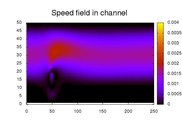
42 Results Exp. setup Sampling Volume SEM image 50 µm 55 µm t = 500 µs Depth of Field ~20 µm 42


43 Results Flow field measurement 100 µl/h 32x32 pixel windows ~ 5.12 µm Simulated velocity Finding c and δ SV-channel intersections Fit residual minima Best fit kinks Average over SV 43


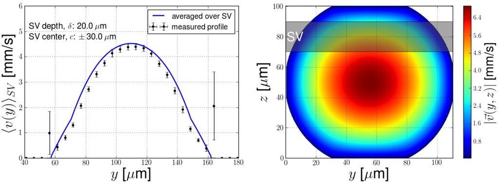

44 Results 44 Flow rate Channel geometry Theoretical velocity field Sampling Volume
45 Examples Robustness against camera misalignment camera x misaligned SV Determine c(x) θ =

46 Examples Robustness against noisy data Dust particle on microfluidic chip 46
47 Examples Robustness against irreproducibility Before disconnecting the pump After reconnecting the pump and refocusing the microscope Two measurements on the same channel and with the same flow rate Moving the channel and refocusing changes the location of the SV and, hence, the measured velocity profile. 47
48 Examples Changing processing algorithms Ensemble average over correlation functions Ensemble average over velocity vectors Velocity profile processed from the exact same set of images, but with different algorithms 48
49 Examples Analysis of Scanning PIV Poiseuille profile Focal plane Microscope objective Maximize velocity for c Laser beam Kloosterman et al., Maximum velocity
50 Conclusion A simple spatial average over the Sampling Volume suffices to explain the discrepancies between expected and measured velocity profiles. The near-wall features such as kinks provide extra information that allow the full determination of flow rates unknown to the experimenter. The Sampling Volume approach provided a straightforward interpretation of the measured data and was able to reproduce the experimental profile from wall to wall. µpiv measurements can be made quantitative without using post-processing. This approach is robust against the most common sources of experimental uncertainty. 50 The Scanning PIV procedure fails to locate the center of the channel for large DOC.
51 Acknowledgements Michael Engel from IBM Research Watson for the SEM images. Diney Ether from LPO UFRJ for helping with the calibration. José Florián from PUC Rio for help with the µpiv equipment. Angelo Gobbi from LMF - LNNano for profilometer measurements Contact: rneumann@br.ibm.com 51

52 Thank You! 52
IBM Research - Zurich Research Laboratory
 October 28, 2010 IBM Research - Zurich Research Laboratory Walter Riess Science & Technology Department IBM Research - Zurich wri@zurich.ibm.com Outline IBM Research IBM Research Zurich Science & Technology
The Transformative Power of Technology
 Dr. Bernard S. Meyerson, IBM Fellow, Vice President of Innovation, CHQ The Transformative Power of Technology The Roundtable on Education and Human Capital Requirements, Feb 2012 Dr. Bernard S. Meyerson,
Particle Image Velocimetry
 Markus Raffel Christian E. Willert Steve T. Wereley Jiirgen Kompenhans Particle Image Velocimetry A Practical Guide Second Edition With 288 Figures and 42 Tables < J Springer Contents Preface V 1 Introduction
Learning to see the Forest and the Trees (A systematic approach to driving innovation) Dr. Bernard S. Meyerson Chief Innovation Officer IBM
 Dr. Bernard S. Meyerson Chief Innovation Officer IBM") Learning to see the Forest and the Trees (A systematic approach to driving innovation) Dr. Bernard S. Meyerson Chief Innovation Officer IBM Corporation Why Innovate? What is the most important capability
Learning to see the Forest and the Trees (A systematic approach to driving innovation) Dr. Bernard S. Meyerson Chief Innovation Officer IBM Corporation Why Innovate? What is the most important capability
Wirelessly powered micro-tracer enabled by miniaturized antenna and microfluidic channel
 Journal of Physics: Conference Series PAPER OPEN ACCESS Wirelessly powered micro-tracer enabled by miniaturized antenna and microfluidic channel To cite this article: G Duan et al 2015 J. Phys.: Conf.
IBM Research Zurich. A Strategy of Open Innovation. Dr. Jana Koehler, Manager Business Integration Technologies. IBM Research Zurich
 IBM Research Zurich A Strategy of Open Innovation Dr., Manager Business Integration Technologies IBM A Century of Information Technology Founded in 1911 Among the leaders in the IT industry in every decade
IBM Research Your future is our concern IBM Corporation
 Your future is our concern A call for action 3.7 billion lost hours 8.7 billion liters of gas Annual impact of congested roadways in the U.S. alone An IBM Research answer 20% less traffic Traffic system:
Lecture 20: Optical Tools for MEMS Imaging
 MECH 466 Microelectromechanical Systems University of Victoria Dept. of Mechanical Engineering Lecture 20: Optical Tools for MEMS Imaging 1 Overview Optical Microscopes Video Microscopes Scanning Electron
Figure 1: A detailed sketch of the experimental set up.
 Electronic Supplementary Material (ESI) for Soft Matter. This journal is The Royal Society of Chemistry 2015 Supplementary Information Detailed Experimental Set Up camera 2 long range objective aluminum
History of PIV Development in JAPAN
 History of PIV Development in JAPAN Koji OKAMOTO The University of Tokyo okamoto@k.u-tokyo.ac.jp okamoto@utvis.com Flow Visualization Society of Japan Founded in 1981 (National Workshop from 1973) 1 st
Bias errors in PIV: the pixel locking effect revisited.
 Bias errors in PIV: the pixel locking effect revisited. E.F.J. Overmars 1, N.G.W. Warncke, C. Poelma and J. Westerweel 1: Laboratory for Aero & Hydrodynamics, University of Technology, Delft, The Netherlands,
Great Minds. Internship Program IBM Research - China
 Internship Program 2017 Internship Program 2017 Jump Start Your Future at IBM Research China Introduction invites global candidates to apply for the 2017 Great Minds internship program located in Beijing
COMPUTER SCIENCE AND ENGINEERING
 COMPUTER SCIENCE AND ENGINEERING Internet of Thing Cloud Computing Big Data Analytics Network Security Distributed System Image Processing Data Science Business Intelligence Wireless Sensor Network Artificial
Femtosecond laser microfabrication in. Prof. Dr. Cleber R. Mendonca
 Femtosecond laser microfabrication in polymers Prof. Dr. Cleber R. Mendonca laser microfabrication focus laser beam on material s surface laser microfabrication laser microfabrication laser microfabrication
Nanotechnology, the infrastructure, and IBM s research projects
 Nanotechnology, the infrastructure, and IBM s research projects Dr. Paul Seidler Coordinator Nanotechnology Center, IBM Research - Zurich Nanotechnology is the understanding and control of matter at dimensions
write-nanocircuits Direct-write Jaebum Joo and Joseph M. Jacobson Molecular Machines, Media Lab Massachusetts Institute of Technology, Cambridge, MA
 Fab-in in-a-box: Direct-write write-nanocircuits Jaebum Joo and Joseph M. Jacobson Massachusetts Institute of Technology, Cambridge, MA April 17, 2008 Avogadro Scale Computing / 1 Avogadro number s? Intel
Astigmatism Particle Tracking Velocimetry for Macroscopic Flows
 1TH INTERNATIONAL SMPOSIUM ON PARTICLE IMAGE VELOCIMETR - PIV13 Delft, The Netherlands, July 1-3, 213 Astigmatism Particle Tracking Velocimetry for Macroscopic Flows Thomas Fuchs, Rainer Hain and Christian
Advanced 3D Optical Profiler using Grasshopper3 USB3 Vision camera
 Advanced 3D Optical Profiler using Grasshopper3 USB3 Vision camera Figure 1. The Zeta-20 uses the Grasshopper3 and produces true color 3D optical images with multi mode optics technology 3D optical profiling
Fast Raman Spectral Imaging Using Chirped Femtosecond Lasers
 Fast Raman Spectral Imaging Using Chirped Femtosecond Lasers Dan Fu 1, Gary Holtom 1, Christian Freudiger 1, Xu Zhang 2, Xiaoliang Sunney Xie 1 1. Department of Chemistry and Chemical Biology, Harvard
CHAPTER 6 CARBON NANOTUBE AND ITS RF APPLICATION
 CHAPTER 6 CARBON NANOTUBE AND ITS RF APPLICATION 6.1 Introduction In this chapter we have made a theoretical study about carbon nanotubes electrical properties and their utility in antenna applications.
Introduction to Electronic Devices
 (Course Number 300331) Fall 2006 Instructor: Dr. Dietmar Knipp Assistant Professor of Electrical Engineering Information: http://www.faculty.iubremen.de/dknipp/ Source: Apple Ref.: Apple Ref.: IBM Critical
Design of a Wide-Bandwidth on-chip Antenna for Uncooled Passive THz Imaging
 RZ 3844 (# Z1302-01) 02/28/2032 Electrical Engineering 5 pages Research Report Design of a Wide-Bandwidth on-chip Antenna for Uncooled Passive THz Imaging Bernhard Klein 1,3, Thomas Morf 1, Michel Despont
Introduction to Microfluidics. C. Fütterer, Institut Curie & Fluigent SA, Paris
 Introduction to Microfluidics C. Fütterer, Institut Curie & Fluigent SA, Paris Miniaturisation & Integration Micro-Pipettes Problems: Minimal volume: 1μl Samples unprotected against evaporation & contamination
Micromachined Floating Element Hydrogen Flow Rate Sensor
 Micromachined Floating Element Hydrogen Flow Rate Sensor Mark Sheplak Interdisciplinary Microsystems Group Mechanical and Aerospace Engineering Department University of Florida Start Date = 09/30/04 Planned
Feature-level Compensation & Control
 Feature-level Compensation & Control 2 Sensors and Control Nathan Cheung, Kameshwar Poolla, Costas Spanos Workshop 11/19/2003 3 Metrology, Control, and Integration Nathan Cheung, UCB SOI Wafers Multi wavelength
Progress due to: Feature size reduction - 0.7X/3 years (Moore s Law). Increasing chip size - 16% per year. Creativity in implementing functions.
. Increasing chip size - 16% per year. Creativity in implementing functions.") Introduction - Chapter 1 Evolution of IC Fabrication 1960 and 1990 integrated t circuits. it Progress due to: Feature size reduction - 0.7X/3 years (Moore s Law). Increasing chip size - 16% per year. Creativity
Introduction - Chapter 1 Evolution of IC Fabrication 1960 and 1990 integrated t circuits. it Progress due to: Feature size reduction - 0.7X/3 years (Moore s Law). Increasing chip size - 16% per year. Creativity
Park NX-Hivac The world s most accurate and easy to use high vacuum AFM for failure analysis.
 Park NX-Hivac The world s most accurate and easy to use high vacuum AFM for failure analysis www.parkafm.com Park NX-Hivac High vacuum scanning for failure analysis applications 4 x 07 / Cm3 Current (µa)
3D Optical Motion Analysis of Micro Systems. Heinrich Steger, Polytec GmbH, Waldbronn
 3D Optical Motion Analysis of Micro Systems Heinrich Steger, Polytec GmbH, Waldbronn SEMICON Europe 2012 Outline Needs and Challenges of measuring Micro Structure and MEMS Tools and Applications for optical
Real-Time Scanning Goniometric Radiometer for Rapid Characterization of Laser Diodes and VCSELs
 Real-Time Scanning Goniometric Radiometer for Rapid Characterization of Laser Diodes and VCSELs Jeffrey L. Guttman, John M. Fleischer, and Allen M. Cary Photon, Inc. 6860 Santa Teresa Blvd., San Jose,
Manipulation, Assembly & Characterization. of Optically Functional 1-D Organic. Nanostructures.
 1 Manipulation, Assembly & Characterization of Optically Functional 1-D Organic Nanostructures. Authors: Ken Reynolds, P. Lovera, D. Iacopino, H. Doyle, A. O Riordan, G. Redmond. Nanotechnology Group Tyndall
Advanced Nanoscale Metrology with AFM
 Advanced Nanoscale Metrology with AFM Sang-il Park Corp. SPM: the Key to the Nano World Initiated by the invention of STM in 1982. By G. Binnig, H. Rohrer, Ch. Gerber at IBM Zürich. Expanded by the invention
A Novel Surgery-like Strategy for Droplet Coalescence in Microchannels
 Supplementary Material (ESI) for Lab on a Chip A Novel Surgery-like Strategy for Droplet Coalescence in Microchannels Supplementary material Nan-Nan Deng, a Shao-Xing Sun, a Wei Wang, a Xiao-Jie Ju, a
NANOELECTRONIC TECHNOLOGY: CHALLENGES IN THE 21st CENTURY
 NANOELECTRONIC TECHNOLOGY: CHALLENGES IN THE 21st CENTURY S. M. SZE National Chiao Tung University Hsinchu, Taiwan And Stanford University Stanford, California ELECTRONIC AND SEMICONDUCTOR INDUSTRIES
III III 0 IIOI DID IIO 1101 I II 0II II 100 III IID II DI II
 (19) United States III III 0 IIOI DID IIO 1101 I0 1101 0II 0II II 100 III IID II DI II US 200902 19549A1 (12) Patent Application Publication (10) Pub. No.: US 2009/0219549 Al Nishizaka et al. (43) Pub.
EPD ENGINEERING PRODUCT DEVELOPMENT
 EPD PRODUCT DEVELOPMENT PILLAR OVERVIEW The following chart illustrates the EPD curriculum structure. It depicts the typical sequence of subjects. Each major row indicates a calendar year with columns
PIV STUDY OF STANDING WAVES IN A RESONANT AIR COLUMN
 PIV STUDY OF STANDING WAVES IN A RESONANT AIR COLUMN Pacs: 43.58.Fm, 43.20.Ye, 43.20.Ks Tonddast-Navaei, Ali; Sharp, David Open University Department of Environmental and Mechanical Engineering, Open University,
This list supersedes the one published in the November 2002 issue of CR.
 PERIODICALS RECEIVED This is the current list of periodicals received for review in Reviews. International standard serial numbers (ISSNs) are provided to facilitate obtaining copies of articles or subscriptions.
Impact of the light coupling on the sensing properties of photonic crystal cavity modes Kumar Saurav* a,b, Nicolas Le Thomas a,b,
 Impact of the light coupling on the sensing properties of photonic crystal cavity modes Kumar Saurav* a,b, Nicolas Le Thomas a,b, a Photonics Research Group, Ghent University-imec, Technologiepark-Zwijnaarde
Towards a Reconfigurable Nanocomputer Platform
 Towards a Reconfigurable Nanocomputer Platform Paul Beckett School of Electrical and Computer Engineering RMIT University Melbourne, Australia 1 The Nanoscale Cambrian Explosion Disparity: Widerangeof
Compressed-air flow control system
 Supplementary Information Supplementary Material (ESI) for Lab on a Chip Compressed-air flow control system Ki Wan Bong a, Stephen C. Chapin a, Daniel C. Pregibon b, David Baah c, Tamara M. Floyd-Smith
Image sensor combining the best of different worlds
 Image sensors and vision systems Image sensor combining the best of different worlds First multispectral time-delay-and-integration (TDI) image sensor based on CCD-in-CMOS technology. Introduction Jonathan
The energy and sustainability concentration emphasizes the mechanical aspects of energy conversion and management.
 Elective Concentrations The program in Mechanical Engineering is designed to appeal to students with a wide variety of interests and professional goals. By an appropriate choice of elective courses, students
Digital Photographic Imaging Using MOEMS
 Digital Photographic Imaging Using MOEMS Vasileios T. Nasis a, R. Andrew Hicks b and Timothy P. Kurzweg a a Department of Electrical and Computer Engineering, Drexel University, Philadelphia, USA b Department
Particles Depth Detection using In-Line Digital Holography Configuration
 Particles Depth Detection using In-Line Digital Holography Configuration Sanjeeb Prasad Panday 1, Kazuo Ohmi, Kazuo Nose 1: Department of Information Systems Engineering, Graduate School of Osaka Sangyo
Detection of Obscured Targets
 Detection of Obscured Targets Waymond R. Scott, Jr. and James Mcclellan School of Electrical and Computer Engineering Georgia Institute of Technology Atlanta, GA 30332-0250 waymond.scott@ece.gatech.edu
Digital Camera Technologies for Scientific Bio-Imaging. Part 2: Sampling and Signal
 Digital Camera Technologies for Scientific Bio-Imaging. Part 2: Sampling and Signal Yashvinder Sabharwal, 1 James Joubert 2 and Deepak Sharma 2 1. Solexis Advisors LLC, Austin, TX, USA 2. Photometrics
Direct observation of beamed Raman scattering
 Supporting Information Direct observation of beamed Raman scattering Wenqi Zhu, Dongxing Wang, and Kenneth B. Crozier* School of Engineering and Applied Sciences, Harvard University, Cambridge, Massachusetts
Mode analysis of Oxide-Confined VCSELs using near-far field approaches
 Annual report 998, Dept. of Optoelectronics, University of Ulm Mode analysis of Oxide-Confined VCSELs using near-far field approaches Safwat William Zaki Mahmoud We analyze the transverse mode structure
Measurement of channel depth by using a general microscope based on depth of focus
 Eurasian Journal of Analytical Chemistry Volume, Number 1, 007 Measurement of channel depth by using a general microscope based on depth of focus Jiangjiang Liu a, Chao Tian b, Zhihua Wang c and Jin-Ming
Super High Vertical Resolution Non-Contact 3D Surface Profiler BW-S500/BW-D500 Series
 Super High Vertical Resolution Non-Contact 3D Surface Profiler BW-S500/BW-D500 Series Nikon's proprietary scanning-type optical interference measurement technology achieves 1pm* height resolution. * Height
SENSOR+TEST Conference SENSOR 2009 Proceedings II
 B8.4 Optical 3D Measurement of Micro Structures Ettemeyer, Andreas; Marxer, Michael; Keferstein, Claus NTB Interstaatliche Hochschule für Technik Buchs Werdenbergstr. 4, 8471 Buchs, Switzerland Introduction
Investigation of an optical sensor for small angle detection
 Investigation of an optical sensor for small angle detection usuke Saito, oshikazu rai and Wei Gao Nano-Metrology and Control Lab epartment of Nanomechanics Graduate School of Engineering, Tohoku University
Confocal Imaging Through Scattering Media with a Volume Holographic Filter
 Confocal Imaging Through Scattering Media with a Volume Holographic Filter Michal Balberg +, George Barbastathis*, Sergio Fantini % and David J. Brady University of Illinois at Urbana-Champaign, Urbana,
Nicolet Almega XR. High Performance Micro and Macro Dispersive Raman Analysis Systems
 m o l e c u l a r s p e c t r o s c o p y Nicolet Almega XR High Performance Micro and Macro Dispersive Raman Analysis Systems Materials Research Identification/Verification Characterization Failure Analysis
SPRAY DROPLET SIZE MEASUREMENT
 SPRAY DROPLET SIZE MEASUREMENT In this study, the PDA was used to characterize diesel and different blends of palm biofuel spray. The PDA is state of the art apparatus that needs no calibration. It is
3D light microscopy techniques
 3D light microscopy techniques The image of a point is a 3D feature In-focus image Out-of-focus image The image of a point is not a point Point Spread Function (PSF) 1D imaging 1 1 2! NA = 0.5! NA 2D imaging
Development of a High-speed Super-resolution Confocal Scanner
 Development of a High-speed Super-resolution Confocal Scanner Takuya Azuma *1 Takayuki Kei *1 Super-resolution microscopy techniques that overcome the spatial resolution limit of conventional light microscopy
Innovative Technology for Innovative Science Hands-on in a Nanoscience Classroom
 Innovative Technology for Innovative Science Hands-on in a Nanoscience Classroom Presented by Jennifer F. Wall, Ph.D. Imaging Possibilities Optical 2 mm Electron 500 microns Atomic Force 10 microns Scanning
ECE-606: Spring Course Introduction
 ECE-606: Spring 2013 Course Introduction Professor Mark Lundstrom Electrical and Computer Engineering Purdue University, West Lafayette, IN USA lundstro@purdue.edu 1/8/13 1 course objectives To introduce
shaping global nanofuture ULTRA-PRECISE PRINTING OF NANOMATERIALS
 shaping global nanofuture ULTRA-PRECISE PRINTING OF NANOMATERIALS WHO ARE WE? XTPL S.A. is a company operating in the nanotechnology segment. The interdisciplinary team of XTPL develops on a global scale
Camera Overview. Digital Microscope Cameras for Material Science: Clear Images, Precise Analysis. Digital Cameras for Microscopy
 Digital Cameras for Microscopy Camera Overview For Materials Science Microscopes Digital Microscope Cameras for Material Science: Clear Images, Precise Analysis Passionate about Imaging: Olympus Digital
IMI Labs Semiconductor Applications. June 20, 2016
 IMI Labs Semiconductor Applications June 20, 2016 Materials Are At the Core of Innovation in the 21st Century Weight Space Flexibility Heat Management Lightweight Energy Efficient Temperature Energy Efficient
Video Microscopy of Selective Laser Sintering. Abstract
 Video Microscopy of Selective Laser Sintering Lawrence S. Melvin III, Suman Das, and Joseph J. Beaman Jr. Department of Mechanical Engineering The University of Texas at Austin Abstract This paper presents
All-Glass Gray Scale PhotoMasks Enable New Technologies. Che-Kuang (Chuck) Wu Canyon Materials, Inc.
 Wu Canyon Materials, Inc.") All-Glass Gray Scale PhotoMasks Enable New Technologies Che-Kuang (Chuck) Wu Canyon Materials, Inc. 1 Overview All-Glass Gray Scale Photomask technologies include: HEBS-glasses and LDW-glasses HEBS-glass
All-Glass Gray Scale PhotoMasks Enable New Technologies Che-Kuang (Chuck) Wu Canyon Materials, Inc. 1 Overview All-Glass Gray Scale Photomask technologies include: HEBS-glasses and LDW-glasses HEBS-glass
USING PIV ON THE SPLASH WATER IN A PELTON TURBINE
 USING PIV ON THE SPLASH WATER IN A PELTON TURBINE B.List, J.Prost, H.-B. Matthias Institute for Waterpower and Pumps Vienna University of Technology 1040 Wien, Austria Abstract: At the Institute for Waterpower
Carbon Nanotube Bumps for Thermal and Electric Conduction in Transistor
 Carbon Nanotube Bumps for Thermal and Electric Conduction in Transistor V Taisuke Iwai V Yuji Awano (Manuscript received April 9, 07) The continuous miniaturization of semiconductor chips has rapidly improved
Measurement of Microscopic Three-dimensional Profiles with High Accuracy and Simple Operation
 238 Hitachi Review Vol. 65 (2016), No. 7 Featured Articles Measurement of Microscopic Three-dimensional Profiles with High Accuracy and Simple Operation AFM5500M Scanning Probe Microscope Satoshi Hasumura
GRADUATE PROGRAMMES Semester 2 Examination EXAM TIMETABLE
 PAGE: 1 OF 10 12-Mar-2018 (Mon) SBS TUTORIAL ROOM TR+5 BS7010 PRACTICAL COURSE IN ELECTRON MICROSCOPY & IMAGE PROCESSING OF MACROMOLECULAR COMPLEXES 12-Apr-2018 (Thu) SBS CLASSROOM 4 BS7005 PRACTICAL COURSE
Chromatic X-Ray imaging with a fine pitch CdTe sensor coupled to a large area photon counting pixel ASIC
 Chromatic X-Ray imaging with a fine pitch CdTe sensor coupled to a large area photon counting pixel ASIC R. Bellazzini a,b, G. Spandre a*, A. Brez a, M. Minuti a, M. Pinchera a and P. Mozzo b a INFN Pisa
Highly Sensitive Filter-Less Fluorescence Detection Method Using an Avalanche Photodiode
 Journal of Energy and Power Engineering 10 (2016) 268-273 doi: 10.17265/1934-8975/2016.04.008 D DAVID PUBLISHING Highly Sensitive Filter-Less Fluorescence Detection Method Using an Avalanche Photodiode
Doppler-Free Spetroscopy of Rubidium
 Doppler-Free Spetroscopy of Rubidium Pranjal Vachaspati, Sabrina Pasterski MIT Department of Physics (Dated: April 17, 2013) We present a technique for spectroscopy of rubidium that eliminates doppler
TechSearch International, Inc. Corporate Overview E. Jan Vardaman, President
 TechSearch International, Inc. Corporate Overview E. Jan Vardaman, President Corporate Background Founded in 1987 and headquartered in Austin, Texas Recognized around the world as a leading consulting
Unit-25 Scanning Tunneling Microscope (STM)
") Unit-5 Scanning Tunneling Microscope (STM) Objective: Imaging formation of scanning tunneling microscope (STM) is due to tunneling effect of quantum physics, which is in nano scale. This experiment shows
Unit-5 Scanning Tunneling Microscope (STM) Objective: Imaging formation of scanning tunneling microscope (STM) is due to tunneling effect of quantum physics, which is in nano scale. This experiment shows
Snapshot Mask-less fabrication of embedded monolithic SU-8 microstructures with arbitrary topologies
 Snapshot Mask-less fabrication of embedded monolithic SU-8 microstructures with arbitrary topologies Pakorn Preechaburana and Daniel Filippini Linköping University Post Print N.B.: When citing this work,
Optical Micrometer Measurement System Product Description
 Optical Micrometer Measurement System Product Description Virginia Semiconductor Incorporated Fredericksburg, VA 22401 www.virginiasemi.com; www.opticalmicrometer.com (540) 373-2900. OMMS Engineering and
3D light microscopy techniques
 3D light microscopy techniques The image of a point is a 3D feature In-focus image Out-of-focus image The image of a point is not a point Point Spread Function (PSF) 1D imaging 2D imaging 3D imaging Resolution
SUNY Poly in a New Era
 SUNY Poly in a New Era Bahgat Sammakia Interim President, SUNY Polytechnic Institute SUNY Poly in a New Era Overview SUNY Poly is recognized as a global leader in advanced electronics Research and Development,
A 3D Profile Parallel Detecting System Based on Differential Confocal Microscopy. Y.H. Wang, X.F. Yu and Y.T. Fei
 Key Engineering Materials Online: 005-10-15 ISSN: 166-9795, Vols. 95-96, pp 501-506 doi:10.408/www.scientific.net/kem.95-96.501 005 Trans Tech Publications, Switzerland A 3D Profile Parallel Detecting
Introduction course in particle image velocimetry
 Introduction course in particle image velocimetry Olle Törnblom March 3, 24 Introduction Particle image velocimetry (PIV) is a technique which enables instantaneous measurement of the flow velocity at
Course Outcome of M.Tech (VLSI Design)
") Course Outcome of M.Tech (VLSI Design) PVL108: Device Physics and Technology The students are able to: 1. Understand the basic physics of semiconductor devices and the basics theory of PN junction. 2.
Course Outcome of M.Tech (VLSI Design) PVL108: Device Physics and Technology The students are able to: 1. Understand the basic physics of semiconductor devices and the basics theory of PN junction. 2.
Fabrication of Probes for High Resolution Optical Microscopy
 Fabrication of Probes for High Resolution Optical Microscopy Physics 564 Applied Optics Professor Andrès La Rosa David Logan May 27, 2010 Abstract Near Field Scanning Optical Microscopy (NSOM) is a technique
Introduction to VLSI ASIC Design and Technology
 Introduction to VLSI ASIC Design and Technology Paulo Moreira CERN - Geneva, Switzerland Paulo Moreira Introduction 1 Outline Introduction Is there a limit? Transistors CMOS building blocks Parasitics
EPD ENGINEERING PRODUCT DEVELOPMENT
 EPD PRODUCT DEVELOPMENT PILLAR OVERVIEW The following chart illustrates the EPD curriculum structure. It depicts the typical sequence of subjects. Each major row indicates a calendar year with columns
Beyond Photolithography The promise of nano-imprint lithography
 Beyond Photolithography The promise of nano-imprint lithography DISTINGUISHED SPEAKERS Dr. S. V. Sreenivasan (CTO, Molecular Imprints, Inc.) John Pong (Nanonex, Inc.) Dr. Will Tong (Quantum Science Research,
2-10 µm Diameter Water Droplets in Mineral Oil Emulsion Production
 2-10 µm Diameter Water s in Mineral Oil Emulsion Production Dolomite s Generation System - Small s Application Note Page SHPT-487168127-264_v.2.0 Summary 2 Flow Focussing Based Production 3 Experimental
Nanovie. Scanning Tunnelling Microscope
 Nanovie Scanning Tunnelling Microscope Nanovie STM Always at Hand Nanovie STM Lepto for Research Nanovie STM Educa for Education Nanovie Auto Tip Maker Nanovie STM Lepto Portable 3D nanoscale microscope
Silicon Photonics Photo-Detector Announcement. Mario Paniccia Intel Fellow Director, Photonics Technology Lab
 Silicon Photonics Photo-Detector Announcement Mario Paniccia Intel Fellow Director, Photonics Technology Lab Agenda Intel s Silicon Photonics Research 40G Modulator Recap 40G Photodetector Announcement
Diffraction, Fourier Optics and Imaging
 1 Diffraction, Fourier Optics and Imaging 1.1 INTRODUCTION When wave fields pass through obstacles, their behavior cannot be simply described in terms of rays. For example, when a plane wave passes through
Advanced PDK and Technologies accessible through ASCENT
 Advanced PDK and Technologies accessible through ASCENT MOS-AK Dresden, Sept. 3, 2018 L. Perniola*, O. Rozeau*, O. Faynot*, T. Poiroux*, P. Roseingrave^ olivier.faynot@cea.fr *Cea-Leti, Grenoble France;
Analyst. Supplementary Data
 Electronic Supplementary Material (ESI) for Analyst. This journal is The Royal Society of Chemistry 2015 Analyst RSCPublishing Cite this: DOI: 10.1039/x0xx00000x Received 00th January 2015, Accepted 00th
DEPARTMENT OF ELECTRICAL ENGINEERING
 DEPARTMENT OF ELECTRICAL ENGINEERING The department of Electrical Engineering is one of the largest departments in IIT Madras which works in the frontier areas of communications, microgrids, integrated
Nature Structural & Molecular Biology: doi: /nsmb Supplementary Figure 1
 Supplementary Figure 1 Supplemental correlative nanomanipulation-fluorescence traces probing nascent RNA and fluorescent Mfd during TCR initiation. Supplemental correlative nanomanipulation-fluorescence
Phase-sensitive high-speed THz imaging
 Phase-sensitive high-speed THz imaging Toshiaki Hattori, Keisuke Ohta, Rakchanok Rungsawang and Keiji Tukamoto Institute of Applied Physics, University of Tsukuba, 1-1-1 Tennodai, Tsukuba, Ibaraki, 305-8573
NOISE IN MEMS PIEZORESISTIVE CANTILEVER
 NOISE IN MEMS PIEZORESISTIVE CANTILEVER Udit Narayan Bera Mechatronics, IIITDM Jabalpur, (India) ABSTRACT Though pezoresistive cantilevers are very popular for various reasons, they are prone to noise
International Center on Design for Nanotechnology Workshop August, 2006 Hangzhou, Zhejiang, P. R. China
 Challenges and opportunities for Designs in Nanotechnologies International Center on Design for Nanotechnology Workshop August, 2006 Hangzhou, Zhejiang, P. R. China Sankar Basu Program Director Computing
Super-Resolution and Reconstruction of Sparse Sub-Wavelength Images
 Super-Resolution and Reconstruction of Sparse Sub-Wavelength Images Snir Gazit, 1 Alexander Szameit, 1 Yonina C. Eldar, 2 and Mordechai Segev 1 1. Department of Physics and Solid State Institute, Technion,
Instructions for the Experiment
 Instructions for the Experiment Excitonic States in Atomically Thin Semiconductors 1. Introduction Alongside with electrical measurements, optical measurements are an indispensable tool for the study of
Des MEMS aux NEMS : évolution des technologies et des concepts aux travers des développements menés au LETI
 Des MEMS aux NEMS : évolution des technologies et des concepts aux travers des développements menés au LETI Ph. Robert 1 Content LETI at a glance From MEMS to NEMS: 30 years of technological evolution
Innovation for the 21st Century
 Nicholas M. Donofrio IBM Fellow Emeritus (Ret.) IBM Executive VP, Innovation & Technology Innovation for the 21st Century Accelerating Advances in Technology 2 Source: Kurzweil 1999 Moravec 1998 Accelerating
Nanotechnology and its effect on Electronics Manufacturing
 Nanotechnology and its effect on Electronics Manufacturing Dr. Alan Rae Vice President, Market & Business Development, NanoDynamics, Inc. Dr. Robert C. Pfahl, Jr. VP of Operations, inemi Topics Covered