NNCI Computation. Azad Naeemi Georgia Institute of Technology
|
|
|
- Anne Evans
- 5 years ago
- Views:
Transcription


1 NNCI Computation Azad Naeemi Georgia Institute of Technology
2 Modeling and Simulation Modeling and simulation can enhance nanoscale fabrication and characterization: guide experimental research drastically reduce the required number of trial and error iterations enable more in depth interpretation of the characterization results help quantify the true potential value of the fabricated devices 2
3 Current Status Abundance of resources and expertise at various sites even though few sites proposed any activities. Diverse funding sources for development and maintenance of these resources (inadequate in many cases). Ad hoc access and documentation. Many gaps and deficiencies. Duplicate efforts happen. 3
4 NNCI Computation Objectives: To facilitate access to the modeling and simulation capabilities and expertise within NNCI sites. To identify the strategic areas for growth in modeling and simulation To promote and facilitate the development of the new capabilities. An inventory of available modeling and simulation resources and expertise is being complied. The directory is hosted by nanohub.org. So far, 10 sites have reported collectively more than 65 commercial simulation tools and 40 internally developed simulation tools available for internal and/or external users (with and without fee). 8 supercomputers or major computing clusters are available in various sites. 4

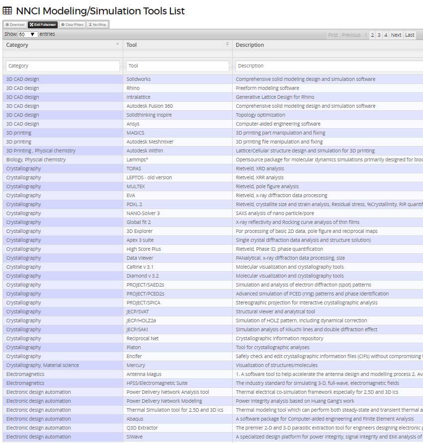
5 Statistics by Disciplines 3D CAD Design 3D Printing Biology Crystallography Electromagnetics Electronic Design Material Science MEMS Microelectronics Microfluidics Nanoelectronics Optics & Photonics Physical Chemistry Process Simulation # OF AVAILABLE TOOLS 5

6 Permission to Access: Commercial Tools Commercial Tool Availability 3D CAD Design 3D Printing Biology Crystallography Electromagnetics Electronic Design Automation Material Science MEMS Microelectronics Microfluidics Nanoelectronics Optics and Photonics Physical Chemistry # OF AVAILABLE TOOLS 6

7 Permission to Access: Internally Developed Tools Internally Developed Tool Availability 3D CAD Design 3D Printing Biology Crystallography Electromagnetics Electronic Design Automation Material Science MEMS Microelectronics Microfluidics Nanoelectronics Optics and Photonics Physical Chemistry # OF AVAILABLE TOOLS 7


8 Contributing Universities ASU Georgia Tech JSNN Northwestern Stanford UCSD University of Louisville University of Nebraska-Lincoln University of Washington UT Austin # OF AVAILABLE TOOLS 8

9 NNCI Computation Group Page on nanohub nanohub.org/groups/nnci_computation 9


10 Spintronic Transport Modeling Tool nanohub.org/tools/spintransport/ Choose right material for your interconnect Use predetermined material parameters OR use your own Obtain electron-spin transport physics-based simulation results 10


11 SPICE Subcircuit Netlist Generator for Spintronic Nonmagnetic Metallic Channel nanohub.org/tools/spincircuit/ Choose right material for your interconnect Use developed compact circuit model for spintronic transport Obtain SPICE subcircuit netlist describing spin&electron transport in channel 11

12 Full Spintronic Device SPICE Netlist Generator on nanohub LLG Solver Subcircuit Models Macromagnetic Solver.subckt 1D Micromagnetic Solver.subckt 2D Micromagnetic Solver.subckt 3D Micromagnetic Solver.subckt Various modules to model and simulate various spintronic devices/circuits in SPICE. Interface Conduction Subcircuit Models Ferro Nonmagnetic Metallic Interface Macro LLG Solver Channel Spintronic Transport Subcircuit Models Electron Transport Spin Transport Spintronic (both electron&spin) Transport 2D LLG Solver Channel Spintronic Transport Interface Conduction 12
13 Simulation Tools from ASU 13
14 NNCI Hardware Resources 8 supercomputers or major computing clusters are available in various sites. All serve internal uses only with the exception of the UT-Austin computing cluster. Example : Partnership for an Advanced Computing Environment (PACE). at GT More than 50,000 cores and more than 8 Petabytes of storage used by approximately 3000 faculty and graduate students. PACE is funded through a mix of central and faculty funding. External users need to fund or collaborate with internal users. 14

15 External Use of ASU Computing Cluster Two International Collaborations with Prof. Vasileska Katerina Raleva UKIM, Macedonia: Multiscale modeling of self-heating effects in heater sensor combination of MOSFETs Gilson Wirth/Alan Rossetto UFRGS, Brazil: Modeling of NBTI in p-channel MOSFETs Multi-scale thermal solver 15
16 Process Simulation Tools Can greatly help users and staff and cut cost. Enable in depth analysis and variability studies Fabrication complexity is growing and user experience is decreasing. Not widely used by users. Plan to hold hands-on workshops to promote Simulate before Fabricate Possible option: Sentaurus TCAD: Fabrication steps: oxidation, diffusion, implantation, etc., Deposition Steps: PVD, CVD, PECVD, etc., Etching processes: Wet etch, RIE, CMP, etc. 16
NNCI Computation. Azad Naeemi Georgia Institute of Technology
 NNCI Computation Azad Naeemi Georgia Institute of Technology azad@gatech.edu Modeling and Simulation Modeling and simulation can enhance nanoscale fabrication and characterization: guide experimental research
CMOS as a Research Platform Progress Report -June 2001 to August 2002-
 CMOS as a Research Platform Progress Report -June 2001 to August 2002- Zhiping (James) Zhou Microelectronics Research Center Georgia Institute of Technology http://cmos.mirc.gatech.edu September 5, 2002
Giovanni Betti Beneventi
 Technology Computer Aided Design (TCAD) Laboratory Lecture 1, Introduction Giovanni Betti Beneventi [Source: Synopsys] E-mail: gbbeneventi@arces.unibo.it ; giobettibeneventi@gmail.com Office: School of
NanoFabrication Kingston. Seminar and Webinar January 31, 2017 Rob Knobel Associate Professor, Dept. of Physics Queen s University
 NanoFabrication Kingston Seminar and Webinar January 31, 2017 Rob Knobel Associate Professor, Dept. of Physics Queen s University What is NFK? It s a place, an team of experts and a service. The goal of
Giovanni Betti Beneventi
 Technology Computer Aided Design (TCAD) Laboratory Lecture 1, Introduction Giovanni Betti Beneventi [Source: Synopsys] E-mail: giovanni.betti2@unibo.it ; giobettibeneventi@gmail.com Office: School of Engineering,
Course Outcome of M.Tech (VLSI Design)
") Course Outcome of M.Tech (VLSI Design) PVL108: Device Physics and Technology The students are able to: 1. Understand the basic physics of semiconductor devices and the basics theory of PN junction. 2.
Course Outcome of M.Tech (VLSI Design) PVL108: Device Physics and Technology The students are able to: 1. Understand the basic physics of semiconductor devices and the basics theory of PN junction. 2.
Scientific Highlights 2016
 Scientific Highlights 2016 Science and Technology Sector Schools and Faculties Faculty of Science Louvain School of Engineering (EPL) Faculty of Architecture, Architectural Engineering and Urban Planning
EE 434 ASIC and Digital Systems. Prof. Dae Hyun Kim School of Electrical Engineering and Computer Science Washington State University.
 EE 434 ASIC and Digital Systems Prof. Dae Hyun Kim School of Electrical Engineering and Computer Science Washington State University Preliminaries VLSI Design System Specification Functional Design RTL
NCN vision NCN vision 2002
 NCN: Global Initiative About "Electronics from the Bottom-up Director Network for Computational Nanotechnology gekco@purdue.edu NCN vision 2002 accelerate the transformation of nanoscience to nanotechnology
Timothy S. Cale, Ph.D ,
 Timothy S. Cale, Ph.D. timothy.cale@gmail.com, 480-381-2228, www.process-evolution.com Objective Provide software tools and consulting services that improve materials and processes. Summary I have extensive
MEDIA RELEASE FOR IMMEDIATE RELEASE 26 JULY 2016
 MEDIA RELEASE FOR IMMEDIATE RELEASE 26 JULY 2016 A*STAR S IME KICKS OFF CONSORTIA TO DEVELOP ADVANCED PACKAGING SOLUTIONS FOR NEXT-GENERATION INTERNET OF THINGS APPLICATIONS AND HIGH-PERFORMANCE WIRELESS
CMOS Digital Integrated Circuits Lec 2 Fabrication of MOSFETs
 CMOS Digital Integrated Circuits Lec 2 Fabrication of MOSFETs 1 CMOS Digital Integrated Circuits 3 rd Edition Categories of Materials Materials can be categorized into three main groups regarding their
IBM Research - Zurich Research Laboratory
 October 28, 2010 IBM Research - Zurich Research Laboratory Walter Riess Science & Technology Department IBM Research - Zurich wri@zurich.ibm.com Outline IBM Research IBM Research Zurich Science & Technology
National Centre for Flexible Electronics
 National Centre for Flexible Electronics Tripartite Partnership Government FlexE Centre - A platform for a meaningful interaction between industry and academia. An interdisciplinary team that advances
International Center on Design for Nanotechnology Workshop August, 2006 Hangzhou, Zhejiang, P. R. China
 Challenges and opportunities for Designs in Nanotechnologies International Center on Design for Nanotechnology Workshop August, 2006 Hangzhou, Zhejiang, P. R. China Sankar Basu Program Director Computing
Nanostencil Lithography and Nanoelectronic Applications
 Microsystems Laboratory Nanostencil Lithography and Nanoelectronic Applications Oscar Vazquez, Marc van den Boogaart, Dr. Lianne Doeswijk, Prof. Juergen Brugger, LMIS1 Dr. Chan Woo Park, Visiting Professor
EPD ENGINEERING PRODUCT DEVELOPMENT
 EPD PRODUCT DEVELOPMENT PILLAR OVERVIEW The following chart illustrates the EPD curriculum structure. It depicts the typical sequence of subjects. Each major row indicates a calendar year with columns
ISMI Industry Productivity Driver
 SEMATECH Symposium Japan September 15, 2010 Accelerating Manufacturing Productivity ISMI Industry Productivity Driver Scott Kramer VP Manufacturing Technology SEMATECH Copyright 2010 SEMATECH, Inc. SEMATECH,
The Cornell NanoScale Facility: NNCI Overview
 The Cornell NanoScale Facility: NNCI Overview Prof. Christopher Ober Lester B. Knight Director CNF: founded 1977 CNF Highlights 2017 is CNF s 40 th Anniversary as an NSF funded User Facility Using NNCI
ROADMAP BACHELOR DEGREE OF ELECTRONIC ENGINEERING WITH HONOURS FACULTY OF ELECTRICAL AND ELECTRONIC ENGINEERING UNIVERSITI TUN HUSSEIN ONN MALAYSIA
 Nationhood Safety Health I Culture BEE 1103 I Islamic Asian BEE 1003 Creativity II Signals Analog s Digital s s I BEE 302 V Fields Waves Power s BEE 302 BEB 303 Circuits s I s I II YEAR Final Year I 1
Mission Statement: Department: Engineering Technology Department Assessment coordinator: Todd Morton
 Department: Engineering Technology Department Assessment coordinator: Todd Morton Mission Statement: The principal mission of the Engineering Technology Department is to provide the highest quality education
LUCEDA PHOTONICS DELIVERS A SILICON PHOTONICS IC SOLUTION IN TANNER L-EDIT
 LUCEDA PHOTONICS DELIVERS A SILICON PHOTONICS IC SOLUTION IN TANNER L-EDIT WIM BOGAERTS, PIETER DUMON, AND MARTIN FIERS, LUCEDA PHOTONICS JEFF MILLER, MENTOR GRAPHICS A M S D E S I G N & V E R I F I C
Variation-Aware Design for Nanometer Generation LSI
 HIRATA Morihisa, SHIMIZU Takashi, YAMADA Kenta Abstract Advancement in the microfabrication of semiconductor chips has made the variations and layout-dependent fluctuations of transistor characteristics
High Performance Computing Systems and Scalable Networks for. Information Technology. Joint White Paper from the
 High Performance Computing Systems and Scalable Networks for Information Technology Joint White Paper from the Department of Computer Science and the Department of Electrical and Computer Engineering With
MEMS in ECE at CMU. Gary K. Fedder
 MEMS in ECE at CMU Gary K. Fedder Department of Electrical and Computer Engineering and The Robotics Institute Carnegie Mellon University Pittsburgh, PA 15213-3890 fedder@ece.cmu.edu http://www.ece.cmu.edu/~mems
Microelectronics Process Engineering at San Jose State University: A Manufacturing-Oriented Interdisciplinary Degree Program
 San Jose State University From the SelectedWorks of David W. Parent March, 2002 Microelectronics Process Engineering at San Jose State University: A Manufacturing-Oriented Interdisciplinary Degree Program
Materials and Material Innovation From FP7 to Horizon 2020
 Materials and Material From FP7 to Horizon 2020 Garmisch Partenkirchen, 10 September 2012 Martin Gieb European Commission martin.gieb@ec.europa.eu DG RTD G3-Materials Unit Europe 2020 Policy Three main
Research Directions in Electrical Engineering
 Research Directions in Electrical Engineering Joseph A. O Sullivan Committee Research Organization Other Universities Future Ad Hoc Committee on Electrical Engineering at Washington University Appointed
Introduction to Microdevices and Microsystems
 PHYS 534 (Fall 2008) Module on Microsystems & Microfabrication Lecture 1 Introduction to Microdevices and Microsystems Srikar Vengallatore, McGill University 1 Introduction to Microsystems Outline of Lecture
Channel Engineering for Submicron N-Channel MOSFET Based on TCAD Simulation
 Australian Journal of Basic and Applied Sciences, 2(3): 406-411, 2008 ISSN 1991-8178 Channel Engineering for Submicron N-Channel MOSFET Based on TCAD Simulation 1 2 3 R. Muanghlua, N. Vittayakorn and A.
AC : EXPERIMENTAL MODULES INTRODUCING MICRO- FABRICATION UTILIZING A MULTIDISCIPLINARY APPROACH
 AC 2011-1595: EXPERIMENTAL MODULES INTRODUCING MICRO- FABRICATION UTILIZING A MULTIDISCIPLINARY APPROACH Shawn Wagoner, Binghamton University Director, Nanofabrication Labatory at Binghamton University,
THE BIOMEDICAL ENGINEERING TEACHING & INNOVATION CENTER. at Boston University s College of Engineering
 THE BIOMEDICAL ENGINEERING TEACHING & INNOVATION CENTER at Boston University s College of Engineering The vision At Boston University s College of Engineering, we intend to create an exciting new resource
MANUFACTURING INSTITUTE
 GEO RG IA TECH MANUFACTURING INSTITUTE Leading manufacturers to successful deployment The Georgia Tech Manufacturing I nstitute will be the world s premier institution anticipating needs and providing
PROCESS AND DEVICE SIMULATION OF 80NM CMOS INVERTER USING SENTAURUS SYNOPSYS TCAD
 052 PROCESS AND DEVICE SIMULATION OF 80NM CMOS INVERTER USING SENTAURUS SYNOPSYS TCAD Muhammad Suhaimi Sulong, Asyiatul Asyikin Jamry, Siti Maryaton Shuadah Shuib, Rahmat Sanudin, Marlia Morsin, Mohd Zainizan
IC1301 -WiPE. Wireless Power Transmission for Sustainable Electronics. SWG4.1: Space Applications. 25 March 2014
 IC1301 -WiPE Wireless Power Transmission for Sustainable Electronics SWG4.1: Space Applications 25 March 2014 Alexandru Takacs CNRS LAAS, Toulouse, France University of Toulouse III Paul Sabatier, France
Introduction to CMC 3D Test Chip Project
 Introduction to CMC 3D Test Chip Project Robert Mallard CMC Microsystems Apr 20, 2011 1 Overview of today s presentation Introduction to the project objectives CMC Why 3D chip stacking? The key to More
Innovation to Advance Moore s Law Requires Core Technology Revolution
 Innovation to Advance Moore s Law Requires Core Technology Revolution Klaus Schuegraf, Ph.D. Chief Technology Officer Silicon Systems Group Applied Materials UC Berkeley Seminar March 9 th, 2012 Innovation
CITATION OF PRESIDENT S SCIENCE AND TECHNOLOGY MEDAL 2012 WINNER
 CITATION OF PRESIDENT S SCIENCE AND TECHNOLOGY MEDAL 2012 WINNER Professor Dim-Lee Kwong Executive Director, Institute of Microelectronics, Agency for Science, Technology and Research (A*STAR) For his
DTU DANCHIP an open access micro/nanofabrication facility bridging academic research and small scale production
 DTU DANCHIP an open access micro/nanofabrication facility bridging academic research and small scale production DTU Danchip National Center for Micro- and Nanofabrication DTU Danchip DTU Danchip is Denmark
The Department of Advanced Materials Engineering. Materials and Processes in Polymeric Microelectronics
 The Department of Advanced Materials Engineering Materials and Processes in Polymeric Microelectronics 1 Outline Materials and Processes in Polymeric Microelectronics Polymeric Microelectronics Process
Consortium Capabilities
 Consortium Capabilities The driver in advanced materials development is to create products with competitive advantages. Products must continuously become faster, lighter and cheaper and must provide additional
Graduate Studies in Computational Science at U-M. Graduate Certificate in Computational Discovery and Engineering. and
 Graduate Studies in Computational Science at U-M Graduate Certificate in Computational Discovery and Engineering and PhD Program in Computational Science Eric Michielssen and Ken Powell 1 Computational
ASPECTS OF HIGH INTEGRATION IN MEMS TECHNOLOGY
 INTERNATIONAL DESIGN CONFERENCE - DESIGN 2006 Dubrovnik - Croatia, May 15-18, 2006. ASPECTS OF HIGH INTEGRATION IN MEMS TECHNOLOGY R. Watty and H. Binz Keywords: methodology, micro-electro-mechanical-systems,
EPD ENGINEERING PRODUCT DEVELOPMENT
 EPD PRODUCT DEVELOPMENT PILLAR OVERVIEW The following chart illustrates the EPD curriculum structure. It depicts the typical sequence of subjects. Each major row indicates a calendar year with columns
Voltage Sag Immunity Compliance Certificate PULS QS10.241, QS A1, QS C1
 PSL File QS10_241 Last modified: 19 December 2011 PSL Power Standards Laboratory www.powerstandards.com 2020 Challenger Drive #100 Alameda, CA 94501 USA TEL ++1-510-522-4400 FAX ++1-510-522-4455 SEMI F47-0706
Machine Learning for Hardware Design. Elyse Rosenbaum University of Illinois at Urbana- Champaign Oct. 18, 2017
 Machine Learning for Hardware Design Elyse Rosenbaum University of Illinois at Urbana- Champaign Oct. 18, 2017 Questions, Questions, Questions 1. How can design productivity be improved? 2. What is machine
Miniature Mid-Infrared Thermooptic Switch with Photonic Crystal Waveguide Based Silicon-on-Sapphire Mach Zehnder Interferometers
 Miniature Mid-Infrared Thermooptic Switch with Photonic Crystal Waveguide Based Silicon-on- Mach Zehnder Interferometers Yi Zou, 1,* Swapnajit Chakravarty, 2,* Chi-Jui Chung, 1 1, 2, * and Ray T. Chen
The State of Innovation. Orlando Saez
 The State of Innovation Orlando Saez Separating fact from myth Myth Illinois is hostile to businesses. Fact Illinois is a good place to do business, and it s getting better everyday. Illinois Economy Highlights
Canada s National Design Network. Community Research Innovation Opportunity
 Canada s National Design Network Community Research Innovation Opportunity Over the past five years, more than 7000 researchers in the National Design Network have benefited from industrial tools, technologies,
Digitisation Plan
 Digitisation Plan 2016-2020 University of Sydney Library University of Sydney Library Digitisation Plan 2016-2020 Mission The University of Sydney Library Digitisation Plan 2016-20 sets out the aim and
Introduction to IEEE CAS Publications
 Introduction to IEEE CAS Publications Gianluca Setti 12 1 Dep. of Engineering (ENDIF) University of Ferrara 2 Advanced Research Center on Electronic Systems for Information Engineering and Telecommunications
College of Engineering Department of Electrical Engineering and Computer Sciences University of California, Berkeley
 College of Engineering Department of Electrical Engineering and Below are your weekly quizzes. You should print out a copy of the quiz and complete it before your lab section. Bring in the completed quiz
Real World Applications on Massively Parallel Environments
 SC12 Nov. 10-16th, 2012 Real World Applications on Massively Parallel Environments YAMAZAKI, Takashi, Ph.D. Application R&D Division Next Generation Technical Computing Unit Fujitsu Ltd. Contents of Presentation
Grand Challenges in Silicon Technology
 Grand Challenges in Silicon Technology Contents: Outcome of Consultation Exercise Page 2 Grand Challenges for Silicon Technology Roadmap Page 5 1 Outcome of Consultation Exercise Executive summary The
NSF Engineering Directorate Overview and Priorities
 NSF Engineering Directorate Overview and Priorities Pramod P. Khargonekar Assistant Director for Engineering National Science Foundation Presentation at USNC/TAM 2015 Annual Meeting May 1, 2015 1 NSF ENG
Electronic sensor for ph measurements in nanoliters
 Electronic sensor for ph measurements in nanoliters Ismaïl Bouhadda, Olivier De Sagazan, France Le Bihan To cite this version: Ismaïl Bouhadda, Olivier De Sagazan, France Le Bihan. Electronic sensor for
A Workshop on Predictive Theoretical and Computational Approaches for Additive Manufacturing
 A Workshop on Predictive Theoretical and Computational Approaches for Additive Manufacturing Keck Center, 500 Fifth St. NW Washington, DC Room K-100 OCTOBER 7-9, 2015 PROGRAM This workshop will focus in
Introducing Technology Computer-Aided Design (TCAD)
") Chinmay K. Maiti Introducing Technology Computer-Aided Design (TCAD) Fundamentals, Simulations, and Applications Introducing Technology Computer-Aided Design (TCAD) Introducing Technology Computer-Aided
Chinmay K. Maiti Introducing Technology Computer-Aided Design (TCAD) Fundamentals, Simulations, and Applications Introducing Technology Computer-Aided Design (TCAD) Introducing Technology Computer-Aided
+1 (479)
") Introduction to VLSI Design http://csce.uark.edu +1 (479) 575-6043 yrpeng@uark.edu Invention of the Transistor Vacuum tubes ruled in first half of 20th century Large, expensive, power-hungry, unreliable
Introduction to VLSI Design http://csce.uark.edu +1 (479) 575-6043 yrpeng@uark.edu Invention of the Transistor Vacuum tubes ruled in first half of 20th century Large, expensive, power-hungry, unreliable
Technology transfer and business development for innovation projects. From local market to global industry.
 Technology transfer and business development for innovation projects. From local market to global industry. www.zntc.ru Well positioned for innovative business development Fab и Lab R&D Multifunctional
Fault Diagnosis Algorithms Part 2
 Fault Diagnosis Algorithms Part 2 By Christopher Henderson Page 1 Fault Diagnosis Algorithms Part 2 Page 5 Technical Tidbit Page 8 Ask the Experts Figure 4. Circuit schematic. This is an example of a circuit
InGaAs MOSFETs for CMOS:
 InGaAs MOSFETs for CMOS: Recent Advances in Process Technology J. A. del Alamo, D. Antoniadis, A. Guo, D.-H. Kim 1, T.-W. Kim 2, J. Lin, W. Lu, A. Vardi and X. Zhao Microsystems Technology Laboratories,
COURSE 2. Mechanical Engineering at MIT
 COURSE 2 Mechanical Engineering at MIT The Department of Mechanical Engineering MechE embodies the Massachusetts Institute of Technology s motto mens et manus, mind and hand as well as heart by combining
ECE 5745 Complex Digital ASIC Design Topic 2: CMOS Devices
 ECE 5745 Complex Digital ASIC Design Topic 2: CMOS Devices Christopher Batten School of Electrical and Computer Engineering Cornell University http://www.csl.cornell.edu/courses/ece5950 Simple Transistor
Des MEMS aux NEMS : évolution des technologies et des concepts aux travers des développements menés au LETI
 Des MEMS aux NEMS : évolution des technologies et des concepts aux travers des développements menés au LETI Ph. Robert 1 Content LETI at a glance From MEMS to NEMS: 30 years of technological evolution
10 COVER FEATURE CAD/EDA FOCUS
 10 COVER FEATURE CAD/EDA FOCUS Effective full 3D EMI analysis of complex PCBs by utilizing the latest advances in numerical methods combined with novel time-domain measurement technologies. By Chung-Huan
Building science, technology and innovation policies
 Map of Europe Building science, technology and innovation policies Prof. Dr. sc. tech. Horst Hippler Rector of the University of Karlsruhe innovasia 2005 Conference & Exhibition 21 23 September 2005 Queen
UVISEL. Spectroscopic Phase Modulated Ellipsometer. The Ideal Tool for Thin Film and Material Characterization
 UVISEL Spectroscopic Phase Modulated Ellipsometer The Ideal Tool for Thin Film and Material Characterization High Precision Research Spectroscopic Ellipsometer The UVISEL ellipsometer offers the best combination
2. The re-examination application link on the portal will be active during the below mentioned period:
 IMPORTANT INSTRUCTIONS TO CANDIDATES 1. All the eligible students who have enrolled in the Academic Year 2014-2015 onwards in the first year of the program are hereby informed to apply for the respective
Instrumentation, Controls, and Automation - Program 68
 Instrumentation, Controls, and Automation - Program 68 Program Description Program Overview Utilities need to improve the capability to detect damage to plant equipment while preserving the focus of skilled
An Information Technology Initiative on. High Aspect Ratio Microsystems Computer-Aided Engineering (HARMCAE) Point of Contact
 Point of Contact") An Information Technology Initiative on High Aspect Ratio Microsystems Computer-Aided Engineering (HARMCAE) Point of Contact Michael C. Murphy, Mechanical Engineering, Ph: 578-5921, email:murphy@me.lsu.edu
An Information Technology Initiative on High Aspect Ratio Microsystems Computer-Aided Engineering (HARMCAE) Point of Contact Michael C. Murphy, Mechanical Engineering, Ph: 578-5921, email:murphy@me.lsu.edu
DISCOVERY LECTURE SERIES
 DISCOVERY LECTURE SERIES 2015 The Discovery Lecture Series is designed to introduce scientific and mathematical research to our students. Guest lectures have agreed to share their knowledge and expertise
SAMPLE SLIDES & COURSE OUTLINE. Core Competency In Semiconductor Technology: 2. FABRICATION. Dr. Theodore (Ted) Dellin
 Dellin") & Digging Deeper Devices, Fabrication & Reliability For More Info:.com or email Dellin@ieee.org SAMPLE SLIDES & COURSE OUTLINE In : 2. A Easy, Effective, of How Devices Are.. Recommended for everyone who
& Digging Deeper Devices, Fabrication & Reliability For More Info:.com or email Dellin@ieee.org SAMPLE SLIDES & COURSE OUTLINE In : 2. A Easy, Effective, of How Devices Are.. Recommended for everyone who
PHGN/CHEN/MLGN 435/535: Interdisciplinary Silicon Processing Laboratory. Simple Si solar Cell!
 Where were we? Simple Si solar Cell! Two Levels of Masks - photoresist, alignment Etch and oxidation to isolate thermal oxide, deposited oxide, wet etching, dry etching, isolation schemes Doping - diffusion/ion
Heterogeneous Technology Alliance. SOI MEMS Platform
 Heterogeneous Technology Alliance SOI MEMS Platform Added value of HTA SOI MEMS Platform to customers 23-Aug-11 Page 1 Attractive offering of HTA SOI MEMS Platform One-stop shop 1 Very extensive R&D resources,
Welcome to ESE Research Interviews 2017
 Dear prospective research student: Welcome to ESE Research Interviews 2017 Thank you for applying for a research student position in our department. The interview s w ill be held on June 5-9, 2017, in
Fabricating 2.5D, 3D, 5.5D Devices
 Fabricating 2.5D, 3D, 5.5D Devices Bob Patti, CTO rpatti@tezzaron.com Tezzar on Semiconduct or 04/15/2013 1 Gen4 Dis-Integrated 3D Memory DRAM layers 42nm node 2 million vertical connections per lay per
A Top-Down Microsystems Design Methodology and Associated Challenges
 A Top-Down Microsystems Design Methodology and Associated Challenges Michael S. McCorquodale, Fadi H. Gebara, Keith L. Kraver, Eric D. Marsman, Robert M. Senger, and Richard B. Brown Department of Electrical
Electrical Engineering Graduate Programs
 Electrical Engineering Graduate Programs I. About the EE College The College of Electrical Engineering (the EE College) of Zhejiang University, one of the ancient electrical engineering departments in
INTRODUCTION TO MICROMACHINING AND MEMS: A LECTURE AND HANDS-ON LABORATORY COURSE FOR UNDERGRADUATE AND GRADUATE STUDENTS FROM ALL BACKGROUNDS
 INTRODUCTION TO MICROMACHINING AND MEMS: A LECTURE AND HANDS-ON LABORATORY COURSE FOR UNDERGRADUATE AND GRADUATE STUDENTS FROM ALL BACKGROUNDS Jack W. Judy and Paulo S. Motta Electrical Engineering Department,
Topic 3. CMOS Fabrication Process
 Topic 3 CMOS Fabrication Process Peter Cheung Department of Electrical & Electronic Engineering Imperial College London URL: www.ee.ic.ac.uk/pcheung/ E-mail: p.cheung@ic.ac.uk Lecture 3-1 Layout of a Inverter
Digital Sustainability: Tyler O. Walters
 Digital Sustainability: Weaving a Tapestry of Interdependency to Advance Digital Programs Tyler O. Walters Associate Director, Technology & Resource Services Georgia Tech Library & Information Center Emory
2018 Research Campaign Descriptions Additional Information Can Be Found at
 2018 Research Campaign Descriptions Additional Information Can Be Found at https://www.arl.army.mil/opencampus/ Analysis & Assessment Premier provider of land forces engineering analyses and assessment
Georgia Tech: Innovation with a Global Footprint
 2012, Georgia Institute of Technology Georgia Tech: Innovation with a Global Footprint Stephen Fleming Vice President @stephenfleming Stephen Fleming 17+ years venture capital investment
Instrumentation and Control
 Program Description Instrumentation and Control Program Overview Instrumentation and control (I&C) and information systems impact nuclear power plant reliability, efficiency, and operations and maintenance
Introduction to Materials Engineering: Materials Driving the Electronics Revolution Robert Hull, MSE
 Introduction to Materials Engineering: Materials Driving the Electronics Revolution Robert Hull, MSE Outline Microelectronics Miniaturization Historical Development: Electronics before Semiconductors The
IEEE TENCON Region 10 Conference Nov, 2016 Marina Bay Sands, Singapore
 IEEE TENCON 2016 Region 10 Conference 22 26 Nov, 2016 Marina Bay Sands, Singapore Conference General Chair: A Alphones IEEE Singapore Section 4 5 Mar 2016 Chiba, Japan Conference Theme for TENCON 2016
Lecture Notes 5 CMOS Image Sensor Device and Fabrication
 Lecture Notes 5 CMOS Image Sensor Device and Fabrication CMOS image sensor fabrication technologies Pixel design and layout Imaging performance enhancement techniques Technology scaling, industry trends
Higher School of Economics, Moscow, Russia. Zelenograd, Moscow, Russia
 Advanced Materials Research Online: 2013-07-31 ISSN: 1662-8985, Vols. 718-720, pp 750-755 doi:10.4028/www.scientific.net/amr.718-720.750 2013 Trans Tech Publications, Switzerland Hardware-Software Subsystem
A School in Computational Science &
 A School in Computational Science & Engineering Richard Fujimoto Chair, Computational Science and Engineering Division Georgia Tech Colleges Architecture Computing Ivan Allen Management Engineering Sciences
Engaging with DARPA. Dr. Stefanie Tompkins. June 9, Distribution Statement A (Approved for Public Release, Distribution Unlimited)
") Engaging with DARPA Dr. Stefanie Tompkins June 9, 2016 DARPA s Mission Breakthrough Technologies for National Security Precision Guidance & Navigation Communications/Networking IR Night Vision Stealth
Engaging with DARPA Dr. Stefanie Tompkins June 9, 2016 DARPA s Mission Breakthrough Technologies for National Security Precision Guidance & Navigation Communications/Networking IR Night Vision Stealth
Preparation of Single Mode Optical Fibers for Application in 3D Interferometry SAMPLE. Applicant: XXXX Date: November 4, 2016
 Preparation of Single Mode Optical Fibers for Application in 3D Interferometry Applicant: XXXX Date: November 4, 2016 Faculty Member: XXXXX Department: Physics Statement of problem/topic of the research
Smart Grid Maturity Model: A Vision for the Future of Smart Grid
 Smart Grid Maturity Model: A Vision for the Future of Smart Grid David W. White Smart Grid Maturity Model Project Manager White is a member of the Resilient Enterprise Management (REM) team in the CERT
Silicon-Based Resonant Microsensors O. Brand, K. Naeli, K.S. Demirci, S. Truax, J.H. Seo, L.A. Beardslee
 Silicon-Based Resonant Microsensors O. Brand, K. Naeli, K.S. Demirci, S. Truax, J.H. Seo, L.A. Beardslee School of Electrical and Computer Engineering g Georgia Institute of Technology Atlanta, GA 30332-0250,
Layout of a Inverter. Topic 3. CMOS Fabrication Process. The CMOS Process - photolithography (2) The CMOS Process - photolithography (1) v o.
 The CMOS Process - photolithography (1) v o.") Layout of a Inverter Topic 3 CMOS Fabrication Process V DD Q p Peter Cheung Department of Electrical & Electronic Engineering Imperial College London v i v o Q n URL: www.ee.ic.ac.uk/pcheung/ E-mail: p.cheung@ic.ac.uk
Layout of a Inverter Topic 3 CMOS Fabrication Process V DD Q p Peter Cheung Department of Electrical & Electronic Engineering Imperial College London v i v o Q n URL: www.ee.ic.ac.uk/pcheung/ E-mail: p.cheung@ic.ac.uk
Validation project Millimeter wave Sensors
 Validation project Millimeter wave Sensors Monitoring of freezing and drying processes as well as the moisture content in food products General project information In a new approved IWT VIS project, called
Nanotechnology, the infrastructure, and IBM s research projects
 Nanotechnology, the infrastructure, and IBM s research projects Dr. Paul Seidler Coordinator Nanotechnology Center, IBM Research - Zurich Nanotechnology is the understanding and control of matter at dimensions
Georgia Electronic Commerce Association. Dr. G. Wayne Clough, President Georgia Institute of Technology April 30, 2003
 Georgia Electronic Commerce Association Dr. G. Wayne Clough, President Georgia Institute of Technology April 30, 2003 Georgia Tech: Driving high-end economic development Oak Ridge National Laboratory National
The Design and Realization of Basic nmos Digital Devices
 Proceedings of The National Conference On Undergraduate Research (NCUR) 2004 Indiana University Purdue University Indianapolis, Indiana April 15-17, 2004 The Design and Realization of Basic nmos Digital
IMI Labs Semiconductor Applications. June 20, 2016
 IMI Labs Semiconductor Applications June 20, 2016 Materials Are At the Core of Innovation in the 21st Century Weight Space Flexibility Heat Management Lightweight Energy Efficient Temperature Energy Efficient