FSA4159 Low-Voltage, 1Ω SPDT Analog Switch with Power-Off Isolation
|
|
|
- Arron Bradley
- 5 years ago
- Views:
Transcription
1 December 2013 FSA4159 Low-Voltage, 1Ω SPDT Analog Switch with Power-Off Isolation Features Low I CC When the S Input is Lower Than V CC Power-Off Isolation (V CC=0 V) 1 Ω On Resistance (R ON) for 4.5 V V CC 0.25 Ω Maximum R ON Flatness for 4.5 V V CC Space-Saving, Pb-Free, 6-Lead SC70 Surface Mount Package Broad V CC Operating Range: 1.65 V to 5.50 V Fast Turn-On and Turn-Of Times Break-Before-Make Enable Circuitry Pb-Free Green Packaging Description The FSA4159 is a high-performance Single-Pole / Double-Throw (SPDT) analog switch. The device features ultra-low R ON of 1 at 4. 5V V CC and operates over the wide V CC range of 1.65 V to 5.50 V. The device is fabricated with sub-micron CMOS technology to achieve fast switching speeds and is designed for break-before-make operation. The FSA4159 features very low quiescent current even when the control voltage is lower than the V CC supply. This feature services mobile handset applications by allowing direct interface with baseband processor general-purpose I/Os. Applications Cellular Phone Portable Media Player PDA Ordering Information Part Number Operating Temperature Range Package FSA4159P6X -40 C to +85 C 6-Lead SC70, EIAJ SC88, 1.25 mm Wide FSA4159L6X -40 C to +85 C 6-Lead MicroPak, 1.00 mm Wide MicroPak is a trademark of Fairchild Semiconductor Corporation. Packing Method 3000 Units on Tape and Reel 5000 Units on Tape and Reel B 1 S GND V CC B 0 A Figure 1. Analog Symbols FSA4159 Rev
2 Pin Configuration B S S 1 6 B1 GND 2 5 V CC V CC 2 5 GND B A A 3 4 B0 Figure 2. SC70 Pin Assignments (Top View) Figure 3. MicroPak Pin Assignment (Top View) Pin Definitions Pin# SC70 Pin# MicroPak Name Description 1 6 B1 Data Ports 2 5 GND Ground 3 4 B0 Data Ports 4 3 A Data Ports 5 2 V CC Supply Voltage 6 1 S Control Input Truth Table Control Input (S) LOW HIGH Function B0 connected to A B1 connected to A FSA4159 Rev
3 Absolute Maximum Ratings Stresses exceeding the absolute maximum ratings may damage the device. The device may not function or be operable above the recommended operating conditions and stressing the parts to these levels is not recommended. In addition, extended exposure to stresses above the recommended operating conditions may affect device reliability. The absolute maximum ratings are stress ratings only. Symbol Parameter Min. Max. Unit V CC Supply Voltage V V sw Switch Voltage (1) -0.5 V CC V V IN Input Voltage (1) V I IK Input Diode Current -50 ma I SW Switch Current (Continuous) 200 ma I SWPEAK Peak Switch Current (Pulsed at 1ms Duration, <10% Duty Cycle) 400 ma P D Power Dissipation at 85 C 180 mw T STG Storage Temperature Range C T J Max Junction Temperature +150 C T L Lead Temperature (Soldering, 10 Seconds) +260 C ESD Human Body Model (JEDEC: JESD22-A114) 4000 Charged Device Model (JEDEC: JESD22-C101) 1500 Machine Model (JEDEC: JESD22-A115) 200 Note: 1. The input and output negative ratings may be exceeded if the input and output diode current ratings are observed. V Recommended Operating Conditions The Recommended Operating Conditions table defines the conditions for actual device operation. Recommended operating conditions are specified to ensure optimal performance to the datasheet specifications. Fairchild does not recommend exceeding them or designing to Absolute Maximum Ratings. Symbol Parameter Min. Max. Unit V CC Supply Voltage V S Control Input Voltage (2) 0 V CC V V SW Switch Input Voltage 0 V CC V T A Operating Temperature C JA Thermal Resistance, Still Air 350 C/W Note: 2. Control Input must be held HIGH or LOW; it must not float. FSA4159 Rev
4 Electrical Characteristics All typical values are at 25 C unless otherwise specified. Symbol Parameter V CC (V) Conditions V IH V IL I IN I NO(0FF), I NC(OFF) I NO(On), I NC(On) I A(ON) I OFF Input Voltage High Input Voltage Low Control Input Leakage Off-Leakage Current of Port B 0 and B 1 On-Leakage Current of Port B 0 and B 1 On Leakage Current of Port A Power Off Leakage Current of Port A & Port B T A=+25 C T A=-40 to +85 C Min. Typ. Max. Min. Max to to to to to to to to V IN=0 or V CC V IN=0 or V CC V IN=0 or V CC V IN=0 or V CC A=1 V, 4.5 V, B 0 or B 1=4.5 C, 1.0 V A=1 V, 3.0 V, B 0 or B 1=3.0 V, 1.0 V A=0.5 V, 2.3 V, B 0 or B 1=2.3 V, 0.5 V A=0.3 V, 1.65 V, B 0 or B 1=1.65 V, 0.3 V A=Float, B 0 or B 1=4.5 V, 1.0 V A=Float, B 0 or B 1=3.0 V, 1.0 V A=Float B 0 or B 1=2.3 V, 0.5 V A=Float, B 0 or B 1=1.65 V, 0.3 V A=1 V,4.5 V B 0 or B 1=1 V, 4.5 V, or Floating A=1 V, 3 V, B 0 or B 1=1 V, 3 V, or Floating A=0.5 V, 2.3 V B 0 or B 1=0.5 V, 2.3 V, or Floating A=0.3 V, 1.65 V B 0 or B 1=0.3 V, 1.65 V, or Floating A=0 to 5.5 V B 0 or B 1=0 to5.5 V Unit V V na na na na ± µa Continued on following page FSA4159 Rev
5 Electrical Characteristics (Continued) All typical values are at 25 C unless otherwise specified. Symbol Parameter V CC (V) Conditions R PEAK R ON R ON R FLAT(ON) I CC Peak On Resistance Switch On Resistance (3) On Resistance Matching Between Channels (4) On Resistance Flatness (5) Quiescent Supply Current I OUT=-100 ma, B 0 or B 1=0 to V CC I OUT=-100 ma, B 0 or B 1=0 to V CC I OUT=-8 ma, B 0 or B 1=0 to V CC I OUT=2 ma, B 0 or B 1=0 to V CC I OUT=-100 ma, B 0 or B 1=2.5 V I OUT=-100 ma, B 0 or B 1=2.0 V I OUT=-8 ma, B 0 or B 1=1.8 V I OUT=-2 ma, B 0 or B 1=1.5 V I OUT=-100 ma, B 0 or B 1=2.5 V I OUT=-100 ma, B 0 or B 1=2.0 V I OUT=-8 ma, B 0 or B 1=1.8 V I OUT=-2 ma B 0 or B 1=1.5 V T A=25, 85 C I OUT=-100 ma, B 0 or B 1=1.0 V, 1.5 V, 2.5 V I OUT=-100 ma, B 0 or B 1=0.8 V, 2.0 V I OUT=-8 ma, B 0 or B 1=0.8 V, 1.8 V I OUT=-2 ma, B 0 or B 1=0.6 V, 1.5 V T A=+25 C T A=-40 to +85 C Min. Typ. Max. Min. Max. T A=-40 C V IN=0 or V CC, I OUT= V IN=0 or V CC, I OUT= V IN=0 or V CC, I OUT= V IN=0 or V CC, I OUT= Notes: 3. On resistance is determined by the voltage drop between A and B pins at the indicated current through the switch. 4. R ON=R ON maximum R ON minimum measured at identical V CC, temperature and voltage. 5. Flatness is defined as the difference between the maximum and minimum value of on resistance over the specified range of conditions. 3.5 Unit Ω Ω Ω Ω na FSA4159 Rev
6 AC Electrical Characteristics All typical value are at V CC=1.8 V, 2.5 V, 3.0 V, 5.0 V at 25 C unless otherwise specified. Symbol Parameter V CC (V) Conditions t ON t OFF t BBM Q Turn-On Time Turn-Off Time Break-Before- Make Time Charge Injection OIRR Off Isolation 1.80 to 5.00 Xtalk Crosstalk 1.80 to 5.00 BW THD -3db Bandwidth Total Harmonic Distortion T A=+25ºC T A=-40to+85ºC Min. Typ. Max. Min. Max to to to 2.70 B 0 or B 1=V CC, R L=50 Ω, C L=35 pf to to to to 2.70 B 0 or B 1=V CC, R L=50 Ω, C L=35 pf to to to to 2.70 B 0 or B 1=V CC, R L=50 Ω, C L=35 pf to C L=1.0 nf, V GEN=0 V, R GEN=0 Ω f=1 MHz, R L=50 Ω f=1 MHz, R L=50 Ω 3.30 R L=50 Ω Unit Figure ns Figure 11 ns Figure 11 ns Figure 12 pc Figure db Figure db Figure R L=600,.006 V IN=0.5 V PP, 5.00 f=20 Hz to 20 khz.002 MHz % Figure 7 Figure 8 Figure 16 Figure 10 Figure 17 Capacitance Symbol Parameter V CC (V) Conditions T A=+25ºC Min. Typ. Max. Unit C IN Control Pin Input Capacitance 0 f=1 MHz, See Figure pf C OFF B Port Off Capacitance 1.65 to 5.50 f=1 MHz, See Figure pf C ON A Port On Capacitance 1.65 to 5.50 f=1 MHz, See Figure pf FSA4159 Rev

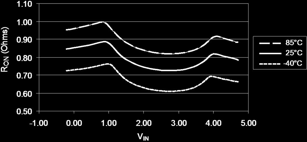
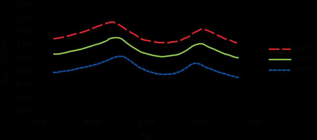
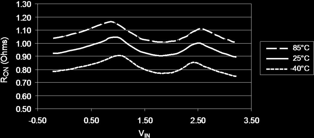

7 Typical Performance Characteristics Figure 4. Switch R ON (V CC=4.5 V) Figure 5. Switch R ON (V CC=3.0 V) Figure 6. Switch R ON (V CC=2.3 V) FSA4159 Rev
8 Gain (db) Gain (db) FSA4159 Low-Voltage, 1 SPDT Analog Switch with Power-Off Isolation Typical Performance Characteristics (Continued) Freqency Response Frequency (MHz) CL = 0pF Figure 7. Frequency Response (C L=0 pf, V CC=5.5 V) Freqency Response Frequency (MHz) CL = 0pF Figure 8. Frequency Response (C L=0 pf, V CC=3.3 V) FSA4159 Rev
9 THD (%) Off Isolation (db) FSA4159 Low-Voltage, 1 SPDT Analog Switch with Power-Off Isolation Typical Performance Characteristics (Continued) Frequency (MHz) Figure 9. Off Isolation (V CC=5.0 V) Frequency (MHz) THD,V CC =1.8V THD, V CC =5.0V Figure 10. Total Harmonic Distortion, Frequency Response (C L=0 pf) FSA4159 Rev


10 Test Diagrams Figure 11. Turn On / Off Timing Figure 12. Break-Before-Make Timing V CC 10nF 0 or V CC S V CC A V IN Network Analyzer OFF-ISOLATION = 20log V OUT V IN ON-LOSS = 20log V OUT V IN 50 B O GND B1 V OUT MEAS REF CROSSTALK = 20log V OUT V IN Figure 13. Off Isolation and Crosstalk FSA4159 Rev


11 Test Diagrams (Continued) Figure 14. Charge Injection Figure 15. On / Off Capacitance Measurement Setup Figure 16. Bandwidth Figure 17. Harmonic Distortion FSA4159 Rev
12 Physical Dimensions 2.00±0.20 A SYMM CL MIN 6 4 B PIN ONE 1.25± (0.25) A B MIN LAND PATTERN RECOMMENDATION SEE DETAIL A C SEATING PLANE 0.10 C 2.10±0.30 NOTES: UNLESS OTHERWISE SPECIFIED GAGE PLANE 0.20 (R0.10) A) THIS PACKAGE CONFORMS TO EIAJ SC-88, B) ALL DIMENSIONS ARE IN MILLIMETERS. C) DIMENSIONS DO NOT INCLUDE BURRS OR MOLD FLASH. D) DRAWING FILENAME: MKT-MAA06AREV DETAIL A SCALE: 60X Figure Lead SC70, EIAJ SC88, 1.25mm Wide Package: Package drawings are provided as a service to customers considering Fairchild components. Drawings may change in any manner without notice. Please note the revision and/or date on the drawing and contact a Fairchild Semiconductor representative to verify or obtain the most recent revision. Package specifications do not expand the terms of Fairchild s worldwide terms and conditions, specifically the warranty therein, which covers Fairchild products. Always visit Fairchild Semiconductor s online packaging area for the most recent package drawings: For current tape and reel specifications, visit Fairchild Semiconductor s online packaging area: FSA4159 Rev
13 Physical Dimensions (Continued) 2X 0.05 C 1.45 B 2X 0.05 C (1) (0.254) 1.00 (0.49) 5X (0.75) PIN 1 IDENTIFIER C DETAIL A TOP VIEW 0.55MAX C X A 0.05 C (0.52) 1X PIN C B A 0.05 C (0.30) 6X RECOMMENED LAND PATTERN X X Notes: (0.05) 6X 0.5 BOTTOM VIEW X 45 CHAMFER 1. CONFORMS TO JEDEC STANDARD M0-252 VARIATION UAAD 2. DIMENSIONS ARE IN MILLIMETERS 3. DRAWING CONFORMS TO ASME Y14.5M FILENAME AND REVISION: MAC06AREV4 5. PIN ONE IDENTIFIER IS 2X LENGTH OF ANY OTHER LINE IN THE MARK CODE LAYOUT. 5X (0.13) 4X DETAIL A PIN 1 TERMINAL Figure Lead, MicroPak 1.0mm Wide Package Package drawings are provided as a service to customers considering Fairchild components. Drawings may change in any manner without notice. Please note the revision and/or date on the drawing and contact a Fairchild Semiconductor representative to verify or obtain the most recent revision. Package specifications do not expand the terms of Fairchild s worldwide terms and conditions, specifically the warranty therein, which covers Fairchild products. Always visit Fairchild Semiconductor s online packaging area for the most recent package drawings: For current tape and reel specifications, visit Fairchild Semiconductor s online packaging area: FSA4159 Rev

14 FSA4159 Rev FSA4159 Low-Voltage, 1 SPDT Analog Switch with Power-Off Isolation
FSA Ω Low-Voltage Dual DPDT Analog Switch
 March 2013 FSA2467 0.4Ω Low-Voltage Dual DPDT Analog Switch Features Typical 0.4 On Resistance (R ON ) for +2.7V Supply Features Less then12µa ICCT Current when Sn Input is Lower than V CC 0.25 Maximum
FSA1259 / FSA1259A Low-Voltage, 1Ω Dual SPST Analog Switch with Power-Off Isolation
 FS1259 / FS1259 Low-Voltage, 1Ω Dual SPST nalog Switch with Power-Off Isolation Features Power-Off Isolation (=0V) 1Ω On Resistance (R ON) for 4.5V 0.25Ω Maximum R ON Flatness for 4.5V Space-Saving, US8
Low-Voltage, 1 Ω Dual SPST Analog Switch with Power-Off Isolation. Description
 FS1259 Low-Voltage, 1 Ω Dual SPST nalog Switch with Power-Off Isolation Features Power-Off Isolation (V CC =0 V) 1 Ω On Resistance (R ON ) for 4.5V V CC 0.25 Ω Maximum R ON Flatness for 4.5 V V CC Space-Saving,
Is Now Part of To learn more about ON Semiconductor, please visit our website at
 Is Now Part of To learn more about ON Semiconductor, please visit our website at www.onsemi.com ON Semiconductor and the ON Semiconductor logo are trademarks of Semiconductor Components Industries, LLC
NC7WZ07 TinyLogic UHS Dual Buffer (Open-Drain Outputs)
") April 2013 NC7WZ07 TinyLogic UHS Dual Buffer (Open-Drain Outputs) Features Ultra-High Speed: t PZL 2.3 ns (Typical) High I OL Output Drive: ±24 ma at 3 CC Broad CC Operating Range: 1.65 to 5.50 Power Down
April 2013 NC7WZ07 TinyLogic UHS Dual Buffer (Open-Drain Outputs) Features Ultra-High Speed: t PZL 2.3 ns (Typical) High I OL Output Drive: ±24 ma at 3 CC Broad CC Operating Range: 1.65 to 5.50 Power Down
NC7SZ66 Low Voltage Single SPST Normally Open Bus Switch
 September 2013 NC7SZ66 Low Voltage Single SPST Normally Open Bus Switch Features Broad V CC Operating Range: 1.65 V to 5.5 V Rail-to-Rail Signal Handling Power Down High-Impedance Inputs/Outputs 5 Ω Switch
FSA Ω Low-Voltage SPDT Analog Switch
 F5157 0.4Ω Low-Voltage PDT nalog witch Features Typical 0.4Ω On Resistance (R ON ) for +2.7V upply F5157 Features Less than 12μ I CCT Current When Input is Lower than 0.25Ω Maximum R ON Flatness for +2.7V
NC7SZ57 / NC7SZ58 TinyLogic UHS Universal Configurable Two-Input Logic Gates
 NC7SZ57 / NC7SZ58 TinyLogic UHS Universal Configurable Two-Input Logic Gates Features Ultra High Speed Capable of Implementing any Two-Input Logic Functions Typical Usage Replaces Two (2) TinyLogic Gate
FSA110 Audio and Wired-OR USB2.0 Hi-Speed (480Mbps) Switch with Negative Signal Capability and Built-in Termination
 Switch with Negative Signal Capability and Built-in Termination") July 2013 FSA110 Audio and Wired-OR USB2.0 Hi-Speed (480Mbps) Switch with Negative Signal Capability and Built-in Termination Features 6pF Typical Switch Off Capacitance for HS USB 2.5Ω Typical On Resistance
July 2013 FSA110 Audio and Wired-OR USB2.0 Hi-Speed (480Mbps) Switch with Negative Signal Capability and Built-in Termination Features 6pF Typical Switch Off Capacitance for HS USB 2.5Ω Typical On Resistance
FSA2269 / FSA2269TS Low-Voltage Dual-SPDT (0.4 ) Analog Switch with Negative Swing Audio Capability
 Analog Switch with Negative Swing Audio Capability") July 2013 FSA2269 / FSA2269TS Low-Voltage Dual-SPDT (0.4 ) Analog Switch with Negative Swing Audio Capability Features 0.4 Ω Typical On Resistance (R ON) for +3.0 V Supply 0.25 Ω Maximum RON Flatness for
July 2013 FSA2269 / FSA2269TS Low-Voltage Dual-SPDT (0.4 ) Analog Switch with Negative Swing Audio Capability Features 0.4 Ω Typical On Resistance (R ON) for +3.0 V Supply 0.25 Ω Maximum RON Flatness for
FSA2268 / FSA2268T Low-Voltage Dual-SPDT (0.4 ) Analog Switch with 16kV ESD
 Analog Switch with 16kV ESD") FSA2268 / FSA2268T Low-Voltage Dual-SPDT (0.4 ) Analog Switch with 16kV ESD Features 0.4Ω Typical On Resistance (R ON) for +3.0V Supply 0.25Ω Maximum R ON Flatness for +3.0V Supply -3db Bandwidth: > 50MHz
FSA2268 / FSA2268T Low-Voltage Dual-SPDT (0.4 ) Analog Switch with 16kV ESD Features 0.4Ω Typical On Resistance (R ON) for +3.0V Supply 0.25Ω Maximum R ON Flatness for +3.0V Supply -3db Bandwidth: > 50MHz
NC7SZ157 TinyLogic UHS 2-Input Non-Inverting Multiplexer
 NC7SZ157 TinyLogic UHS 2-Input Non-Inverting Multiplexer Features Broad CC Operating Range: 1.65 to 5.5 Ultra High-Speed Power Down High-Impedance Inputs/Outputs Over-oltage Tolerance Inputs Facilitate
FSAT66 Low Voltage Single SPST Normally Open Analog Switch with TTL Compatible Control Input
 April 2003 Revised July 2004 FSAT66 Low Voltage Single SPST Normally Open Analog Switch with TTL Compatible Control Input General Description The FSAT66 is a high speed single pole/single throw normally
FSA2859 Dual-Voltage, 0.8Ω DPDT Analog Switch with Power-Off Isolation
 Click here for this datasheet translated into Chinese! ugust 2008 F2859 Dual-Voltage, 0.8Ω DPDT nalog witch with Power-Off Isolation Features Power-Off Isolation (=0V) 0.8Ω Maximum On Resistance (R ON)
WAS4729QB QB* WAS4729QB. Descriptions. Features. Applications. Order information
 WAS4729QB Low On Resistance (0.75Ω) Dual SPDT Analog Switch with Negative Swing Audio Capability Http//:www.sh-willsemi.com Descriptions The WAS4729QB is a high performance, dual Single Pole Double Throw
FSUSB45 High-Speed USB2.0 (480Mbps) Switch with Dedicated Charger Port Detect
 Switch with Dedicated Charger Port Detect") July 2013 FSUSB45 High-Speed USB2.0 (480Mbps) Switch with Dedicated Charger Port Detect Features Low On Capacitance: 7.0 pf Typical Low On Resistance: 3.9 Ω Typical Low Power Consumption: 1 μa Maximum
July 2013 FSUSB45 High-Speed USB2.0 (480Mbps) Switch with Dedicated Charger Port Detect Features Low On Capacitance: 7.0 pf Typical Low On Resistance: 3.9 Ω Typical Low Power Consumption: 1 μa Maximum
NC7WZ16 TinyLogic UHS Dual Buffer
 NC7WZ16 TinyLogic UHS Dual Buffer Features Ultra-High Speed: t PD 2.4ns (Typical) into 50pF at 5 CC High Output Drive: ±24mA at 3 CC Broad CC Operating Range: 1.65 to 5.5 Matches Performance of LCX when
FSUSB43 Low-Power, Two-Port, High-Speed, USB2.0 (480Mbps) Switch
 Switch") FSUSB43 Low-Power, Two-Port, High-Speed, USB2.0 (480Mbps) Switch Features Over-Voltage Tolerance (OVT) on all USB Ports up to 5.25V without External Components Low On Capacitance: 3.7pF Typical Low On
FSUSB43 Low-Power, Two-Port, High-Speed, USB2.0 (480Mbps) Switch Features Over-Voltage Tolerance (OVT) on all USB Ports up to 5.25V without External Components Low On Capacitance: 3.7pF Typical Low On
WAS4723Q WAS4723Q. Order information 1 2 VCC NO1. Low On Resistance, Dual SPDT Analog Switch. Http//: QFN L
 WAS4723Q Low On Resistance, Dual SPDT Analog Switch Http//:www.willsemi.com Descriptions The WAS4723Q is a high performance, dual Single Pole Double Throw (SPDT) analog switch that features ultra-low Ron
NC7SV05 TinyLogic ULP-A Inverter (Open-Drain Output)
") NC7SV05 TinyLogic ULP-A Inverter (Open-Drain Output) Features 0.9V to 3.6V V CC Supply Operation 3.6V Over-Voltage Tolerant I/Os at VCC from 0.9V to 3.6V Extremely High Speed tpd - 1.0ns: Typical for 2.7V
NC7SV05 TinyLogic ULP-A Inverter (Open-Drain Output) Features 0.9V to 3.6V V CC Supply Operation 3.6V Over-Voltage Tolerant I/Os at VCC from 0.9V to 3.6V Extremely High Speed tpd - 1.0ns: Typical for 2.7V
FSUSB45 Hi-Speed USB2.0 (480Mbps) Switch with Dedicated Charger Port Detect
 Switch with Dedicated Charger Port Detect") December 2009 FSUSB45 Hi-Speed USB2.0 (480Mbps) Switch with Dedicated Charger Port Detect Features Low On Capacitance: 7.0pF Typical Low On Resistance: 3.9Ω Typical Low Power Consumption: 1μA Maximum -
December 2009 FSUSB45 Hi-Speed USB2.0 (480Mbps) Switch with Dedicated Charger Port Detect Features Low On Capacitance: 7.0pF Typical Low On Resistance: 3.9Ω Typical Low Power Consumption: 1μA Maximum -
FSA321 USB2.0 Hi-Speed (480Mbps) and Audio Switches with Negative Signal Capability and Built-in Termination on Unselected Audio Paths
 and Audio Switches with Negative Signal Capability and Built-in Termination on Unselected Audio Paths") March 2013 FSA321 USB2.0 Hi-Speed (480Mbps) and Audio Switches with Negative Signal Capability and Built-in Termination on Unselected Audio Paths Features Audio: 1.8 Typical On Resistance HS-USB: 8 Typical
March 2013 FSA321 USB2.0 Hi-Speed (480Mbps) and Audio Switches with Negative Signal Capability and Built-in Termination on Unselected Audio Paths Features Audio: 1.8 Typical On Resistance HS-USB: 8 Typical
NC7SZ125 TinyLogic UHS Buffer with Three-State Output
 NC7SZ125 TinyLogic UHS Buffer with Three-State Output January 2014 NC7SZ125 TinyLogic UHS Buffer with Three-State Output Features Ultra-High Speed: t PD 2.6 ns (Typical) into 50 pf at 5 CC High Output
FSAV430 Low Voltage 1.1GHz, 4-Channel, 2:1 Video Switch
 FSAV430 Low Voltage 1.1GHz, 4-Channel, 2:1 Video Switch Features -40dB Off Isolation at 30MHz -60dB Non-Adjacent Channel Crosstalk at 30MHz 3dB Bandwidth: 1.1GHz On Resistance: 4.5 (Typical) Low Power
FSA2257 Low R ON Low-Voltage Dual SPDT Bi-Directional Analog Switch
 F2257 Low R ON Low-Voltage Dual PDT Bi-Directional nalog witch Features Maximum 1.15Ω On Resistance (R ON ) for 4.5V upply 0.3Ω Maximum R ON Flatness for +5V upply pace-aving MicroPak Packaging Broad Operating
FSAV MHz, 4-Channel, 2:1 Video Switch
 Features -50dB Off Isolation at 30MHz -80dB Non-Adjacent Channel Crosstalk at 30MHz 3dB Bandwidth: 800MHz On Resistance: 4 (Typical) Low Power Consumption: 1µA (Maximum) Control Input TTL Compatible Applications
WAS4899Q WAS4899Q. Descriptions. Features. Order information. Applications. Low On Resistance, Quad SPDT Analog Switch. Http//:
 WAS4899Q Low On Resistance, Quad SPDT Analog Switch Http//:www.willsemi.com Descriptions The WAS4899Q is a high performance, quad, Single Pole Double Throw (SPDT) analog switch that features ultra-low
NC7SZ08 TinyLogic UHS Two-Input AND Gate
 NC7SZ08 TinyLogic UHS Two-Input AND Gate Features Ultra-High Speed: t PD 2.7ns (Typical) into 50pF at 5 CC High Output Drive: ±24mA at 3 CC Broad CC Operating Range: 1.65 to 5.5 Matches Performance of
PI5A4684. Chip Scale Packaging, Dual SPDT Analog Switch. Features. Description. Pin Configuration/ Block Diagram (top view) CSP.
 CSP.") Features CMOS Technology for Bus and Analog Applications Low On-Resistance: 0.5Ω. Wide Range: 1.65V to 5.5V Rail-to-Rail Signal Range Control Input Overvoltage Tolerance: 5.5V min. High Off Isolation:
Features CMOS Technology for Bus and Analog Applications Low On-Resistance: 0.5Ω. Wide Range: 1.65V to 5.5V Rail-to-Rail Signal Range Control Input Overvoltage Tolerance: 5.5V min. High Off Isolation:
Is Now Part of To learn more about ON Semiconductor, please visit our website at
 Is Now Part of To learn more about ON Semiconductor, please visit our website at www.onsemi.com ON Semiconductor and the ON Semiconductor logo are trademarks of Semiconductor Components Industries, LLC
NC7SZ86 TinyLogic UHS Two-Input Exclusive-OR Gate
 NC7SZ86 TinyLogic UHS Two-Input Exclusive-OR Gate Features Ultra-High Speed: t PD 2.9ns (Typical) into 50pF at 5 CC High Output Drive: ±24mA at 3 CC Broad CC Operating Range: 1.65 to 5.5 Matches Performance
NC7SZ38 TinyLogic UHS 2-Input NAND Gate, Open Drain Output
 NC7SZ38 TinyLogic UHS 2-Input NAND Gate, Open Drain Output Features Ultra-High Speed: t PD 2.4ns (Typical) into 50pF at 5V V CC Open Drain Output Stage for OR Tied Applications High Output Sink Drive:
UM Ω Ultra Low ON-Resistance Dual SPDT Analog Switch UM5223 QFN General Description. Applications
 0.5Ω Ultra Low ON-Resistance Dual SPDT Analog Switch UM5223 QFN10 1.8 1.4 General Description The UM5223 is a low on-resistance (R ON ), dual single-pole/double-throw (SPDT) analog switch operates from
MP2735/MP2736 Low-Voltage 0.45Ω Dual SPDT Analog Switches
 The Future of Analog IC Technology GENERAL DESCRIPTION The MP2735/MP2736 are low voltage, low onresistance, dual single-pole, double-throw (SPDT) monolithic CMOS analog switches designed for high performance
STG3693. Low voltage high bandwidth quad SPDT switch. Features. Description
 Low voltage high bandwidth quad SPDT switch Datasheet - production data Features Ultra low power dissipation: I CC = 0.3 µa at T A = 125 C Low on-resistance: R DS(on) = 4 Ω (T A = 25 C) at V CC = 3.0 V
NC7SZ14 TinyLogic UHS Inverter with Schmitt Trigger Input
 January 2010 NC7SZ14 TinyLogic UHS Inverter with Schmitt Trigger Input Features Ultra-High Speed: t PD 3.7ns (Typical) into 50pF at 5 CC High Output Drive: ±24mA at 3 CC Broad CC Operating Range: 1.65
NC7SZU04 TinyLogic UHS Unbuffered Inverter
 NC7SZU04 TinyLogic UHS Unbuffered Inverter Features Unbuffered for Crystal Oscillator and Analog Applications Balanced Output Drive: ±16mA at 4.5 CC Broad CC Operating Range: 1.65 to 5.5 Matches Performance
FAN4010 High-Side Current Sensor
 November 213 FAN41 High-Side Current Sensor Features a +5 V Low Cost, Accurate, High-Side Current Sensing Output Voltage Scaling Up to 2.5 V Sense Voltage 2 V to 6 V Supply Range 2 μa Typical Offset Current
WAS4732D WAS4732D. Descriptions. Features. Order information. Applications. MIC/GND Cross-point Switch for EU/US Headphone Compatible Application
 / Cross-point Switch for EU/US Headphone Compatible Application http://www.sh-willsemi.com Descriptions The is a 2x2 cross-point switch that is used to interchange the Ground and connections on a headphone
NC7SZ125 TinyLogic UHS Buffer with Three-State Output
 NC7SZ125 TinyLogic UHS Buffer with Three-State Output Features Ultra-High Speed: t PD 2.6ns (Typical) into 50pF at 5 CC High Output Drive: ±24mA at 3 CC Broad CC Operating Range: 1.65 to 5.5 Matches Performance
NC7SZ125 TinyLogic UHS Buffer with Three-State Output
 NC7SZ125 TinyLogic UHS Buffer with Three-State Output Features Ultra-High Speed: t PD 2.6ns (Typical) into 50pF at 5 CC High Output Drive: ±24mA at 3 CC Broad CC Operating Range: 1.65 to 5.5 Matches Performance
NC7SZ74 TinyLogic UHS D-Type, Flip-Flop with Preset and Clear
 NC7SZ74 TinyLogic UHS D-Type, Flip-Flop with Preset and Clear Features Ultra-High Speed: t PD 2.6 (Typical) into 50pF at 5 CC High Output Drive: ±24mA at 3 CC Broad CC Operating Range: 1.65 to 5.5 Power
Features. Applications
 PRELIMINARY DATASHEET IDTHS421V16 Description The IDTHS421V16 is a bi-directional, low power, Quad single-pole, double-throw (SPDT) hybrid switch targeted at dual SIM card multiplexing. It is optimized
FSUSB46 Hi-Speed USB2.0 (480Mbps) DPST Switch with Dedicated Charger Port Detection
 DPST Switch with Dedicated Charger Port Detection") March 2013 FSUSB46 Hi-Speed USB2.0 (480Mbps) DPST Switch with Dedicated harger Port Detection Features Low On apacitance: 7.0pF Typical Low On Resistance: 3.9Ω Typical Low Power onsumption: 1μA Maximum
March 2013 FSUSB46 Hi-Speed USB2.0 (480Mbps) DPST Switch with Dedicated harger Port Detection Features Low On apacitance: 7.0pF Typical Low On Resistance: 3.9Ω Typical Low Power onsumption: 1μA Maximum
NC7SV57 / NC7SV58 TinyLogic ULP-A Universal Configurable Two-Input Logic Gates
 December 2010 NC7S57 / NC7S58 TinyLogic ULP-A Universal Configurable Two-Input Logic Gates Features 0.9 to 3.6 CC Supply Operation 3.6 Over-oltage Tolerant I/Os at CC from 0.9 to 3.6 Extremely High Speed
FSA3031 Dual High-Speed USB2.0 with Mobile High-Definition Link (MHL )
") FSA3031 Dual High-Speed USB2.0 with Mobile High-Definition Link (MHL ) Features Low On Capacitance: 4.6 pf/6.75 pf MHL/USB (Typical) Low Power Consumption: 30 μa Maximum Supports MHL Rev. 2.0 Passes 1080
FSA3031 Dual High-Speed USB2.0 with Mobile High-Definition Link (MHL ) Features Low On Capacitance: 4.6 pf/6.75 pf MHL/USB (Typical) Low Power Consumption: 30 μa Maximum Supports MHL Rev. 2.0 Passes 1080
NC7SZ00 TinyLogic UHS Two-Input NAND Gate
 NC7SZ00 TinyLogic UHS Two-Input NAND Gate Features Ultra-High Speed: t PD 2.4ns (Typical) into 50pF at 5 CC High Output Drive: ±24mA at 3 CC Broad CC Operating Range: 1.65 to 5.5 Matches Performance of
PI5A23159 Low Voltage Dual SPDT 0.8Ω Analog Switch
 Features CMOS Technology for Bus and Analog Applications Low On-Resistance: 0.8 at 3.0V Wide Range: 1.65V to 5.5V Rail-to-Rail Signal Range Control Overvoltage Tolerance: 5.5V(Min) Fast Transition Speed:
FSAV433 High-Bandwidth (550MHz), 3-Channel, 3:1 Video Switch
, 3-Channel, 3:1 Video Switch") January 2011 FSAV433 High-Bandwidth (550MHz), 3-Channel, 3:1 Video Switch Features Ground between Channels to Optimize Isolation and Reduce Hostile Crosstalk -70dB Non-Adjacent Channel Crosstalk at 30MHz
January 2011 FSAV433 High-Bandwidth (550MHz), 3-Channel, 3:1 Video Switch Features Ground between Channels to Optimize Isolation and Reduce Hostile Crosstalk -70dB Non-Adjacent Channel Crosstalk at 30MHz
FSUSB30 Low-Power, Two-Port, High-Speed USB 2.0 (480Mbps) Switch
 Switch") Click to see this datasheet in Simplified Chinese! FSUSB30 Low-Power, Two-Port, High-Speed USB 2.0 (480Mbps) Switch Features Low On Capacitance: 3.7pF (Typical) Low On Resistance: 6.5Ω (Typical) Low Power
Click to see this datasheet in Simplified Chinese! FSUSB30 Low-Power, Two-Port, High-Speed USB 2.0 (480Mbps) Switch Features Low On Capacitance: 3.7pF (Typical) Low On Resistance: 6.5Ω (Typical) Low Power
AS11P2TLR. Low voltage 1 Ω single-pole double-throw analog switch with breakbefore-make. Description. Features
 Low voltage 1 Ω single-pole double-throw analog switch with breakbefore-make feature Description Datasheet - production data Features DFN6L High speed: t PD = 130 ps (typ.) at V CC = 3.0 V t PD = 140 ps
FSUSB22 Low-Power, 2-Port, High-Speed USB 2.0 (480Mbps) Switch
 Switch") March 2008 FSUSB22 Low-Power, 2-Port, High-Speed USB 2.0 (480Mbps) Switch Features -40dB Off Isolation at 250MHz -40dB Non-adjacent Channel Crosstalk at 250MHz On Resistance: 4.5Ω Typical (RON) -3dB Bandwidth:
March 2008 FSUSB22 Low-Power, 2-Port, High-Speed USB 2.0 (480Mbps) Switch Features -40dB Off Isolation at 250MHz -40dB Non-adjacent Channel Crosstalk at 250MHz On Resistance: 4.5Ω Typical (RON) -3dB Bandwidth:
Description. Features. Applications. Pin Assignment. Pin Description Pin No Pin Name. Logic Function Table Logic Inputs(S) PI5A4157
 PI5A4157") Low Voltage SPDT 0.8Ω Analog Switch Features CMOS Technology for Bus and Analog Applications Low On-Resistance: 0.8Ω at 3.0V Wide Range: 1.65V to 5.5V Rail-to-Rail Signal Range Control Input Overvoltage
Low Voltage SPDT 0.8Ω Analog Switch Features CMOS Technology for Bus and Analog Applications Low On-Resistance: 0.8Ω at 3.0V Wide Range: 1.65V to 5.5V Rail-to-Rail Signal Range Control Input Overvoltage
FSA806 USB2.0 High-Speed (480Mbps), UART, and Audio Switch with Negative Signal Capability
, UART, and Audio Switch with Negative Signal Capability") July 2012 FSA806 USB2.0 High-Speed (480Mbps), UART, and Audio Switch with Negative Signal Capability Features 3:1 Switch Handles: - Audio Headsets - UART - Up to Two High- and Low-Speed USB Data Negative-Swing-Capable
July 2012 FSA806 USB2.0 High-Speed (480Mbps), UART, and Audio Switch with Negative Signal Capability Features 3:1 Switch Handles: - Audio Headsets - UART - Up to Two High- and Low-Speed USB Data Negative-Swing-Capable
FST Bit Bus Switch
 Features 4Ω Switch Connection between Two Ports Minimal Propagation Delay through the Switch Low I CC Zero Bounce in Flow-through Mode Control Inputs Compatible with TTL Level Description March 2008 Fairchild
FSUSB73 3:1 High-Speed USB Multiplexer and Hub Routing Switch
 April 2012 FSUSB73 3:1 High-Speed USB Multiplexer and Hub Routing Switch Features Switch Type 3:1 MUX + Isolation Switch USB USB 2.0 High-Speed & Full-Speed Compliant R ON 6.5Ω C ON ESD (IEC61000-4-2)
MM74HC86 Quad 2-Input Exclusive OR Gate
 MM74HC86 Quad 2-Input Exclusive OR Gate Features Typical Propagation Delay: 9ns Wide Operating oltage Range: 2 6 Low Input Current: 1mA Maximum Low Quiescent Current: 20mA Max. (74 Series) Output Drive
SGM Ω, High Speed, Low Voltage Dual, DPDT Analog Switch
 GENERAL DESCRIPTION The SGM44601 is a high-speed, low-voltage, advanced dual-independent double-pole/double-throw (DPDT) CMOS analog switch that is designed to operate from a single +1.8V to +5.5V power
Obsolete Product(s) - Obsolete Product(s) Obsolete Product(s) - Obsolete Product(s) STG3684
 - Obsolete Product(s) Obsolete Product(s) - Obsolete Product(s) STG3684") LOW VOLTAGE 0.5Ω MAX DUAL SPDT SWITCH WITH BREAK BEFORE MAKE FEATURE HIGH SPEED: t PD = 0.3ns (TYP.) at V CC = 3.0V t PD = 0.4ns (TYP.) at V CC = 2.3V ULTRA LOW POWER DISSIPATION: I CC = 0.2µA (MAX.) at
LOW VOLTAGE 0.5Ω MAX DUAL SPDT SWITCH WITH BREAK BEFORE MAKE FEATURE HIGH SPEED: t PD = 0.3ns (TYP.) at V CC = 3.0V t PD = 0.4ns (TYP.) at V CC = 2.3V ULTRA LOW POWER DISSIPATION: I CC = 0.2µA (MAX.) at
STG3699AQTR LOW VOLTAGE 0.5Ω MAX QUAD SPDT SWITCH WITH BREAK-BEFORE-MAKE FEATURE
 LOW VOLTAGE 0.5Ω MAX QUAD SPDT SWITCH WITH BREAK-BEFORE-MAKE FEATURE HIGH SPEED: t PD = 1.5ns (TYP.) at V CC = 3.0V t PD = 1.5ns (TYP.) at V CC = 2.3V ULTRA LOW POWER DISSIPATION: I CC = 0.2µA (MAX.) at
0.39, Low-R ON, Ultra-Low Distortion, Compact DPDT Analog Switch
 .39, Low-R ON, Ultra-Low Distortion, Compact DPDT Analog Switch DESCRIPTION The is a compact, low resistance, ultra-low distortion double pole double throw (DPST) analog switch. The features a flat.39
FEATURES BENEFITS APPLICATIONS. PARAMETER LIMIT UNIT Reference to GND V to +6 IN, COM, NC, NO a -0.3 to (V )
") DESCRIPTION www.vishay.com.5, High Bandwidth, Dual SPDT Analog Switch The DGE is a low-voltage dual single-pole / double-throw monolithic CMOS analog switch. Designed to operate from. V to 5.5 V power
DESCRIPTION www.vishay.com.5, High Bandwidth, Dual SPDT Analog Switch The DGE is a low-voltage dual single-pole / double-throw monolithic CMOS analog switch. Designed to operate from. V to 5.5 V power
SGM Ω, High Speed, Low Voltage Dual, DPDT Analog Switch
 GENERAL DESCRIPTION The SGM4462 is a dual, high-speed, low-voltage, double-pole/double-throw (DPDT) CMOS analog switch that is designed to operate from a single 1.8V to 5.5V power supply. It features high-bandwidth
FSA3200 Two-Port, High-Speed USB2.0 Switch with Mobile High-Definition Link (MHL )
") November 2012 FSA3200 Two-Port, High-Speed USB2.0 Switch with Mobile High-Definition Link (MHL ) Features Low On Capacitance: 2.7 pf / 3.1 pf MHL / USB (Typical) Low Power Consumption: 30μA Maximum Supports
November 2012 FSA3200 Two-Port, High-Speed USB2.0 Switch with Mobile High-Definition Link (MHL ) Features Low On Capacitance: 2.7 pf / 3.1 pf MHL / USB (Typical) Low Power Consumption: 30μA Maximum Supports
FSUSB63 3:1 High-Speed USB 2.0 Switch / Multiplexer
 July 2013 FSUSB63 3:1 High-Speed USB 2.0 Switch / Multiplexer Features Switch Type 3:1 USB Switch USB USB 2.0 High-Speed & Full-Speed Compliant Break-Before-Make Time 126µs R ON 6Ω Typical C ON 6pF Typical
STG5682. Low voltage dual SPDTswitch with negative rail capability. Features. Description
 Low voltage dual SPDTswitch with negative rail capability Features Distortion-free negative signal throughput down to V CC -5.5V Wide operating voltage range: V CC (Opr) = 1.65V to 4.5V single supply Ultra
TOP VIEW COUT1 COM2. Maxim Integrated Products 1
 19-77; Rev ; 7/4.75Ω, Dual SPDT Audio Switch with General Description The dual, single-pole/double-throw (SPDT) switch operates from a single +2V to +5.5V supply and features rail-to-rail signal handling.
NLAS5157. Ultra-Low 0.4 SPDT Analog Switch
 Ultra-Low.4 SPDT Analog Switch The NLAS5157 is Single Pole Double Throw (SPDT) switch designed for audio systems in portable applications. The NLAS5157 features Ultra Low R ON of.4 typical at = V and.15
SGM4684 Chip Scale Packaging, Low-Voltage 0.4Ω, Dual, SPDT Analog Switch
 GENERAL DESCRIPTION The SGM4684 is a dual, low on-resistance, low voltage, bidirectional, single-pole/double-throw (SPDT) CMOS analog switch designed to operate from a single 1.8V to 5.5V power supply.
Low-Voltage, Low R ON, SPDT Audio Switch with Negative Swing Capability
 Low-Voltage, Low R ON, SPDT Audio Switch with Negative Swing Capability DG6, DG63 DESCRIPTION The DG6, DG63 is a low on-resistance, single-pole/ double-throw monolithic CMOS analog switch with negative
SGM MHz, Low Voltage SPDT Analog Switch in 6-pin SC70
 GENERAL DESCRIPTION The SGM3167 is a single, bidirectional, single-pole/ double-throw (SPDT) CMOS analog switches designed to operate from a single 1.8V to 5.5V supply. It features high-bandwidth (600MHz)
FT3001 Reset Timer with Configurable Delay
 FT3001 Reset Timer with Configurable Delay Features Delay Times: 3.0, 3.75, 4.5, 6.0 Seconds 1 µa I CC Current Consumption in Standby Primary and Secondary Input Reset Pins Push-Pull and Open-Drain Output
SGM3003 Ultra Low ON-Resistance, Low Voltage, SPDT Analog Switch
 GENERAL DESCRIPTION The SGM3003 is a single, low on-resistance, low voltage, bidirectional, single-pole/double-throw (SPDT) CMOS analog switch designed to operate from a single +1.8V to +5.5V supply. Targeted
SGM3717 4Ω, 400MHz Bandwidth, Dual, SPDT Negative Signal Handling Analog Switch
 Preliminary datasheet SGM3717 GENERAL DESCRIPTION The SGM3717 is a dual, bidirectional, single-pole/ double-throw (SPDT) CMOS analog switch designed to operate from a single +2.5V to +5.0V supply. It features
FAN156 Low Voltage Comparator
 FAN156 Low Voltage Comparator Features Low Supply Current: I DD 6μA (Typical) Single Power Supply Operation Wide Common-Mode Input Voltage Range Push-Pull Output Circuit Low Input Bias Current Internal
STG3699B. Low voltage 0.5 Ω max, quad SPDT switch with break-before-make feature. Features. Description
 Low voltage 0.5 Ω max, quad SPDT switch with break-before-make feature Features High speed: t PD = 1.5 ns (typ.) at V CC = 3.0 V t PD = 1.5 ns (typ.) at V CC = 2.3 V Ultra low power dissipation: I CC =0.2μA
Is Now Part of To learn more about ON Semiconductor, please visit our website at
 Is Now Part of To learn more about ON Semiconductor, please visit our website at www.onsemi.com ON Semiconductor and the ON Semiconductor logo are trademarks of Semiconductor Components Industries, LLC
FAN5622 / FAN5624 / FAN5626 Linear LED Drivers with Single-Wire Digital Interface
 FAN5622 / FAN5624 / FAN5626 Linear LED Drivers with Single-Wire Digital Interface Features Family of Three Linear Current-Sink LED Drivers that Support 2, 4, or 6 LED Outputs Current Sink Driver for Each
TOP VIEW COM2. Maxim Integrated Products 1
 19-3472; Rev ; 1/4 Quad SPST Switches General Description The quad single-pole/single-throw (SPST) switch operates from a single +2V to +5.5V supply and can handle signals greater than the supply rail.
FAN5640 Dual High-Side Constant Current Source for High-Voltage Keypad LED Illumination
 March 2012 FAN5640 Dual High-Side Constant Current Source for High-Voltage Keypad LED Illumination Features 20V Maximum Driver Input Level Dual Output 25mA Drive Capability per Channel Two Strings of 2-4
0.4, Low Resistance and Capacitance, Dual DPDT / Quad SPDT Analog Switch
 .4, Low Resistance and Capacitance, Dual DPDT / Quad SPDT Analog Switch DESCRIPTION The DG2523 and DG2524 are four-channel single-pole double-throw (SPDT) analog switches. The DG2523 has two control inputs
Is Now Part of To learn more about ON Semiconductor, please visit our website at
 Is Now Part of To learn more about ON Semiconductor, please visit our website at www.onsemi.com ON Semiconductor and the ON Semiconductor logo are trademarks of Semiconductor Components Industries, LLC
SGM Ω, High Speed, Low Voltage Dual, DPDT Analog Switch
 GENERAL DESCRIPTION The SGM4461 is a high-speed, low-voltage, advanced dual-independent double-pole/double-throw (DPDT) CMOS analog switch that is designed to operate from a single +1.8V to +5.5V power
74AC14, 74ACT14 Hex Inverter with Schmitt Trigger Input
 74AC14, 74ACT14 Hex Inverter with Schmitt Trigger Input Features I CC reduced by 50% Outputs source/sink 24mA 74ACT14 has TTL-compatible inputs Ordering Information Order Number General Description Package
NC7SZ32 -TinyLogic UHS Two-Input OR Gate
 NC7SZ32 TinyLogic UHS Two-Input OR Gate Features Ultra-High Speed: t PD 2.4ns (Typical) into 50pF at 5V V CC High Output Drive: ±24mA at 3V V CC Broad V CC Operating Range: 1.65V to 5.5V Matches Performance
NC7WZ04/D. TinyLogic UHS Dual Inverter. NC7WZ04 TinyLogic UHS Dual Inverter. Features. Description. Ordering Information. Connection Diagrams
 NC7WZ04 TinyLogic UHS Dual Inverter Features Ultra-High Speed: t PD 2.3ns (Typical) into 50pF at 5 CC High Output Drive: ±24mA at 3 CC Broad CC Operating Range: 1.65 to 5.5 Matches Performance of LCX w
FSUSB20 Low-Power 1-Port High-Speed USB (480Mbps) Switch
 Switch") FSUSB20 Low-Power 1-Port High-Speed USB (480Mbps) Switch Features 30dB off isolation at 250MHz 30dB non-adjacent channel crosstalk at 250MHz 4.5Ω typical on resistance (R ON ) 3dB bandwidth: >720MHz Low
FSUSB20 Low-Power 1-Port High-Speed USB (480Mbps) Switch Features 30dB off isolation at 250MHz 30dB non-adjacent channel crosstalk at 250MHz 4.5Ω typical on resistance (R ON ) 3dB bandwidth: >720MHz Low
Automotive 125 C Analog Switch Dual DPDT / Quad SPDT, 0.37, 338 MHz Bandwidth
 Automotive 125 C Analog Switch Dual DPDT / Quad SPDT, 0.37, 338 MHz Bandwidth DESCRIPTION The, is a four-channel single-pole double-throw (SPDT) analog switch with two control inputs. It is also known
STG3693. Low voltage high bandwidth Quad SPDT switch. Features. Description
 Low voltage high bandwidth Quad SPDT switch Features Ultra low power dissipation: I CC = 0.2μA (Max.) at T A = 85 C Low ON resistance: R ON = 4Ω (T A = 25 C) at V CC = 3.0V Wide operating voltage range:
Dual SPDT Analog Switch
 Dual SPDT Analog Switch DESCRIPTION The DG9236 is a CMOS, dual SPDT analog switch designed to operate from = 2.7 V to = 6 V max. operating, single supply. All control logic inputs have a guaranteed.8 V
SGM Ω, High Speed, Low Voltage Dual, DPDT Analog Switch
 GENERAL DESCRIPTION The SGM44601 is a high-speed, low-voltage, advanced dual-independent double-pole/double-throw (DPDT) CMOS analog switch that is designed to operate from a single +1.8V to +5.5V power
NC7SB3257 TinyLogic UHS 2:1 Multiplexer/Demultiplexer Bus Switch
 TinyLogic UHS 2:1 Multiplexer/Demultiplexer Bus Switch General Description The NC7SB3257 is a high performance, 2:1 NMOS passgate multiplexer/demultiplexer from Fairchild s Ultra High Speed Series of TinyLogic.
0.3 pc Charge Injection, 100 pa Leakage CMOS ± 5 V / 5 V / 3 V Dual SPDT Analog Switch
 0.3 pc Charge Injection, pa Leakage CMOS ± 5 / 5 / 3 Dual SPDT Analog Switch DESCRIPTION The is a dual SPDT CMOS, analog switch, designed to operate from a +3 to +16 single supply, or from ± 3 to ± 8,
SGM Ω, Low Voltage Quad, SPDT Analog Switch
 GENERAL DESCRIPTION The SGM3699 is a quad, low on-resistance, low voltage, bidirectional, single-pole/double-throw (SPDT) CMOS analog switch that is designed to operate from a single 1.8V to 4.35V power
NC7WZ17 TinyLogic UHS Dual Buffer with Schmitt Trigger Inputs
 January 2012 NC7WZ17 TinyLogic UHS Dual Buffer with Schmitt Trigger Inputs Features Ultra-High Speed: t PD 3.6ns (Typical) into 50pF at 5 CC High Output Drive: ±24m at 3 CC Broad CC Operating Range: 1.65
AOZ Ω Low-Voltage Dual-DPDT Analog Switch. General Description. Features. Applications AOZ6275
 .35Ω Low-Voltage Dual-DPDT nalog witch General Description The OZ6275 is a dual Double-Pole, Double-Throw (DPDT) analog switch that is designed to operate from a single 1.65 V to 4.3 V supply. The OZ6275
DG2706. High Speed, Low Voltage, 3, Quad SPDT CMOS Analog Switch. Vishay Siliconix DESCRIPTION FEATURES APPLICATIONS
 High Speed, Low Voltage, 3, Quad SPDT CMOS Analog Switch DESCRIPTION The DG2706 is a high speed, low voltage, low On-resistance, quad SPDT (single pole double throw) analog switch. It operates from a.6
PI5A121/PI5A122/PI5A124
 es Features Single-Supply Operation (+V to +6V) Rail-to-Rail Analog Signal Dynamic Range Low On-Resistance (6Ω typ. with 5V supply) Minimizes Distortion and Error Voltages On-Resistance Flatness, Ω typ.
Sub-Ω, Low Voltage, SPDT Analog Switches with Over Current Protection
 New Product DG/DG1 Sub-Ω, Low Voltage, SPDT Analog Switches with Over Current Protection DESCRIPTION The DG/DG1 are low-voltage single single-pole/ double-throw monolithic CMOS analog switches. Designed
0.5 pc Charge Injection, 100 pa Leakage, Dual SPDT Analog Switch
 0.5 pc Charge Injection, pa Leakage, Dual SPDT Analog Switch DESCRIPTION The is an analog CMOS, dual SPDT switch, designed to operate from a +2.7 V to +12 V single supply or from ± 2.7 V to ± 5 V, dual