Etching Small Samples and the Effects of Using a Carrier Wafer STS ICP-RIE
|
|
|
- Edmund Richard
- 5 years ago
- Views:
Transcription
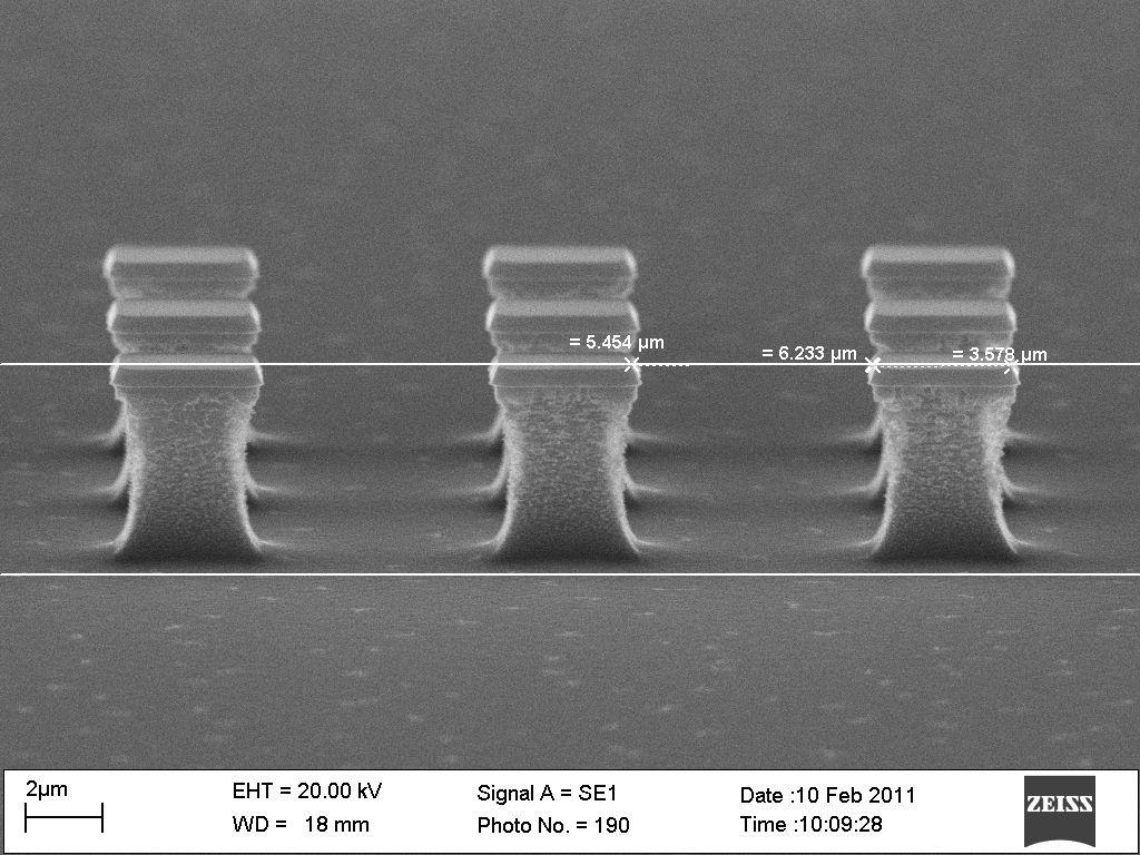
1 Etching Small Samples and the Effects of Using a Carrier Wafer STS ICP-RIE This note is a brief description of the effects of bonding pieces to a carrier wafer during the etch process on the STS ICP-RIE. Users looking to etch Si on samples other than 100mm round Si wafers are required to mount their samples on a carrier wafer. The most common situations are users etching smaller die such as those used in e-beam lithography, or processes which require deep (>250um) Si etching due to the fragility of thinned wafers. As illustrated by the data and images below, the best bonding methods were either the or the photoresist, and using a Si wafer with a protective film. In this case a SiO2 layer on Si was used, but photoresist or other materials will have a similar effect, due to the reduction of exposed Si. The process for bonding using is to melt the (MP = 66oC) by heating the carrier wafer using a hotplate. A spot slightly smaller than the piece to be etched should be melted near the centre of the wafer, and the piece set on the melted. Remove the wafer from the hotplate and allow the substrate to cool. Once cooled, the will have hardened and the wafer will be ready for etching. Once etched, the crystalbond can be removed by soaking in a hot water bath, but may require sonication. If using HPR504 (or a similar resist), use a q-tip and place a drop or two of resist on the backside of the piece or directly on the wafer. Alternatively the resist can be spun over the entire wafer surface. Place the piece on the wafer, and press the piece to spread the resist. Bake the wafer using the litho hotplates for at least 5 minutes at 115oC to fully bake the resist. If the resist is not fully baked, any remaining liquid will form bubbles under the piece when placed under vacuum. This will likely lift the piece from the wafer, and will result in poor thermal conduction and a poor etch. Once etched, the resist can be removed by soaking in acetone, but again may require sonication. Both double-sided tape and kapton tape did not work well for this process. Although using these is a more simple and cleaner method of bonding, the lack of thermal conduction resulted in poor etching. Each adhesive has its pros and cons, it's up to the user to prioritize and decide what works best for their own process. The main issue with using a carrrier wafer is the sensitivity of the etch to wafer temperature. The chuck is cooled to 10C, with the wafer mechanically clamped to the chuck and Helium flowed between the wafer and the chuck to ensure good thermal contact. Stacking two pieces of Si together using some sort of adhesive will inevitably change the wafer temperature and in turn the actual etch. Two sets of runs were performed, one set using the above adhesion methods on a bare Si wafer, and one set using the same methods on a Si wafer with an SiO2 layer to illustrate the effects of the amount of total exposed Si on the overall etch rate. The samples used were small Si die, ~1cm x 1cm, with an SiO2 mask, bonded near the centre of the wafer, each die containing a variety of features. The Precision etch was processed for 5 minutes, and each die measured and imaged for comparison. Note that the etch rate and selectivity obtained during this process are to be used as a guidline only. The actual value will be differnt for all users, and is dependent on a number of items. Refer to other documentation for further information.
2 Etch Rate Etch Rate (um/min) Si Wafer SiO2 Wafer Double sided tape Kapton tape Bond Type Figure 1 Etch Rate of different bonding methods Selectivity 60 Selectivity (Si:SiO2) Si Wafer SiO2 Wafer Double sided tape Bond Type Figure 2 Selectivity of different bonding methods Kapton tape

3 Images: 5um posts on each die were imaged for comparison. This etch was done on a full 100mm wafer using the same mask as the smaller die.


4 Si Wafer Bonding Double Sided Tape Kapton Tape


5 SiO2 Wafer Bonding Double Sided Tape Kapton Tape
HEX02 EMBOSSING SYSTEM
 HEX02 EMBOSSING SYSTEM LOCATION: Hot Embossing Area PRIMARY TRAINER: 1. Scott Munro (2-4826, smunro@ualberta.ca) OVERVIEW The hot embosser is available to users who require polymer mold fabrication. This
KMPR 1010 Process for Glass Wafers
 KMPR 1010 Process for Glass Wafers KMPR 1010 Steps Protocol Step System Condition Note Plasma Cleaning PVA Tepla Ion 10 5 mins Run OmniCoat Receipt Dehydration Any Heat Plate 150 C, 5 mins HMDS Coating
Obducat NIL 6. Nanoimprinting with NRF s NIL 6
 Obducat NIL 6 Substrates: pieces to 6 inch, hard or soft Thermal cure with PMMA, MR I 7010 etc Alignment to about 3 microns Temperature to 300 HC Pressure 15 to 80 bars Resolution < 50 nm possible Up to
Development of a LFLE Double Pattern Process for TE Mode Photonic Devices. Mycahya Eggleston Advisor: Dr. Stephen Preble
 Development of a LFLE Double Pattern Process for TE Mode Photonic Devices Mycahya Eggleston Advisor: Dr. Stephen Preble 2 Introduction and Motivation Silicon Photonics Geometry, TE vs TM, Double Pattern
(ksaligner & quintel resolution)
") Process [4.10] (ksaligner & quintel resolution) 1.0 Process Summary 1.1 Since Karl Suss ksaligner is heavily used and Quintel aligner is not, nanolab decided to compare the 2 micron line resolution from
Process [4.10] (ksaligner & quintel resolution) 1.0 Process Summary 1.1 Since Karl Suss ksaligner is heavily used and Quintel aligner is not, nanolab decided to compare the 2 micron line resolution from
DOE Project: Resist Characterization
 DOE Project: Resist Characterization GOAL To achieve high resolution and adequate throughput, a photoresist must possess relatively high contrast and sensitivity to exposing radiation. The objective of
FINDINGS. REU Student: Philip Garcia Graduate Student Mentor: Anabil Chaudhuri Faculty Mentor: Steven R. J. Brueck. Figure 1
 FINDINGS REU Student: Philip Garcia Graduate Student Mentor: Anabil Chaudhuri Faculty Mentor: Steven R. J. Brueck A. Results At the Center for High Tech Materials at the University of New Mexico, my work
Part 5-1: Lithography
 Part 5-1: Lithography Yao-Joe Yang 1 Pattern Transfer (Patterning) Types of lithography systems: Optical X-ray electron beam writer (non-traditional, no masks) Two-dimensional pattern transfer: limited
Major Fabrication Steps in MOS Process Flow
 Major Fabrication Steps in MOS Process Flow UV light Mask oxygen Silicon dioxide photoresist exposed photoresist oxide Silicon substrate Oxidation (Field oxide) Photoresist Coating Mask-Wafer Alignment
450mm patterning out of darkness Backend Process Exposure Tool SOKUDO Lithography Breakfast Forum July 10, 2013 Doug Shelton Canon USA Inc.
 450mm patterning out of darkness Backend Process Exposure Tool SOKUDO Lithography Breakfast Forum 2013 July 10, 2013 Doug Shelton Canon USA Inc. Introduction Half Pitch [nm] 2013 2014 2015 2016 2017 2018
Lecture 7. Lithography and Pattern Transfer. Reading: Chapter 7
 Lecture 7 Lithography and Pattern Transfer Reading: Chapter 7 Used for Pattern transfer into oxides, metals, semiconductors. 3 types of Photoresists (PR): Lithography and Photoresists 1.) Positive: PR
Semiconductor Manufacturing Technology. Semiconductor Manufacturing Technology. Photolithography: Resist Development and Advanced Lithography
 Semiconductor Manufacturing Technology Michael Quirk & Julian Serda October 2001 by Prentice Hall Chapter 15 Photolithography: Resist Development and Advanced Lithography Eight Basic Steps of Photolithography
Nanostencil Lithography and Nanoelectronic Applications
 Microsystems Laboratory Nanostencil Lithography and Nanoelectronic Applications Oscar Vazquez, Marc van den Boogaart, Dr. Lianne Doeswijk, Prof. Juergen Brugger, LMIS1 Dr. Chan Woo Park, Visiting Professor
CMOS Digital Integrated Circuits Lec 2 Fabrication of MOSFETs
 CMOS Digital Integrated Circuits Lec 2 Fabrication of MOSFETs 1 CMOS Digital Integrated Circuits 3 rd Edition Categories of Materials Materials can be categorized into three main groups regarding their
EE C245 / ME C218 INTRODUCTION TO MEMS DESIGN FALL 2011 PROBLEM SET #2. Due (at 7 p.m.): Tuesday, Sept. 27, 2011, in the EE C245 HW box in 240 Cory.
: Tuesday, Sept. 27, 2011, in the EE C245 HW box in 240 Cory.") Issued: Tuesday, Sept. 13, 2011 PROBLEM SET #2 Due (at 7 p.m.): Tuesday, Sept. 27, 2011, in the EE C245 HW box in 240 Cory. 1. Below in Figure 1.1 is a description of a DRIE silicon etch using the Marvell
Issued: Tuesday, Sept. 13, 2011 PROBLEM SET #2 Due (at 7 p.m.): Tuesday, Sept. 27, 2011, in the EE C245 HW box in 240 Cory. 1. Below in Figure 1.1 is a description of a DRIE silicon etch using the Marvell
Lecture 0: Introduction
 Lecture 0: Introduction Introduction Integrated circuits: many transistors on one chip. Very Large Scale Integration (VLSI): bucketloads! Complementary Metal Oxide Semiconductor Fast, cheap, low power
+ Preferred material for tool O Acceptable material for tool X Unacceptable material for tool
 Contact Aligners (HTG, ABM, EV620) GCA 5X g-line Stepper GCA i-line Steppers (GCA 10X, AS200) Shipley 1800 Series (1805, 1813, 1818, 1827) + + X AZ nlof 2000 O X + AZ4903 + + X OiR 620-7i X X + OiR 897-12i
Outline. 1 Introduction. 2 Basic IC fabrication processes. 3 Fabrication techniques for MEMS. 4 Applications. 5 Mechanics issues on MEMS MDL NTHU
 Outline 1 Introduction 2 Basic IC fabrication processes 3 Fabrication techniques for MEMS 4 Applications 5 Mechanics issues on MEMS 2.2 Lithography Reading: Runyan Chap. 5, or 莊達人 Chap. 7, or Wolf and
Photolithography Technology and Application
 Photolithography Technology and Application Jeff Tsai Director, Graduate Institute of Electro-Optical Engineering Tatung University Art or Science? Lind width = 100 to 5 micron meter!! Resolution = ~ 3
Semiconductor Back-Grinding
 Semiconductor Back-Grinding The silicon wafer on which the active elements are created is a thin circular disc, typically 150mm or 200mm in diameter. During diffusion and similar processes, the wafer may
EE4800 CMOS Digital IC Design & Analysis. Lecture 1 Introduction Zhuo Feng
 EE4800 CMOS Digital IC Design & Analysis Lecture 1 Introduction Zhuo Feng 1.1 Prof. Zhuo Feng Office: EERC 730 Phone: 487-3116 Email: zhuofeng@mtu.edu Class Website http://www.ece.mtu.edu/~zhuofeng/ee4800fall2010.html
Dr. Dirk Meyners Prof. Wagner. Wagner / Meyners Micro / Nanosystems Technology
 Micro/Nanosystems Technology Dr. Dirk Meyners Prof. Wagner 1 Outline - Lithography Overview - UV-Lithography - Resolution Enhancement Techniques - Electron Beam Lithography - Patterning with Focused Ion
Fabrication Techniques of Optical ICs
 Fabrication Techniques of Optical ICs Processing Techniques Lift off Process Etching Process Patterning Techniques Photo Lithography Electron Beam Lithography Photo Resist ( Microposit MP1300) Electron
EG2605 Undergraduate Research Opportunities Program. Large Scale Nano Fabrication via Proton Lithography Using Metallic Stencils
 EG2605 Undergraduate Research Opportunities Program Large Scale Nano Fabrication via Proton Lithography Using Metallic Stencils Tan Chuan Fu 1, Jeroen Anton van Kan 2, Pattabiraman Santhana Raman 2, Yao
Technology for the MEMS processing and testing environment. SUSS MicroTec AG Dr. Hans-Georg Kapitza
 Technology for the MEMS processing and testing environment SUSS MicroTec AG Dr. Hans-Georg Kapitza 1 SUSS MicroTec Industrial Group Founded 1949 as Karl Süss KG GmbH&Co. in Garching/ Munich San Jose Waterbury
Feature-level Compensation & Control
 Feature-level Compensation & Control 2 Sensors and Control Nathan Cheung, Kameshwar Poolla, Costas Spanos Workshop 11/19/2003 3 Metrology, Control, and Integration Nathan Cheung, UCB SOI Wafers Multi wavelength
Dicing Through Hard and Brittle Materials in the Micro Electronic Industry By Gideon Levinson, Dicing Tools Product Manager
 Dicing Through Hard and Brittle Materials in the Micro Electronic Industry By Gideon Levinson, Dicing Tools Product Manager A high percentage of micro electronics dicing applications require dicing completely
+1 (479)
") Introduction to VLSI Design http://csce.uark.edu +1 (479) 575-6043 yrpeng@uark.edu Invention of the Transistor Vacuum tubes ruled in first half of 20th century Large, expensive, power-hungry, unreliable
Introduction to VLSI Design http://csce.uark.edu +1 (479) 575-6043 yrpeng@uark.edu Invention of the Transistor Vacuum tubes ruled in first half of 20th century Large, expensive, power-hungry, unreliable
VLSI Design. Introduction
 VLSI Design Introduction Outline Introduction Silicon, pn-junctions and transistors A Brief History Operation of MOS Transistors CMOS circuits Fabrication steps for CMOS circuits Introduction Integrated
High Power RF MEMS Switch Technology
 High Power RF MEMS Switch Technology Invited Talk at 2005 SBMO/IEEE MTT-S International Conference on Microwave and Optoelectronics Conference Dr Jia-Sheng Hong Heriot-Watt University Edinburgh U.K. 1
Semiconductor Technology
 Semiconductor Technology from A to Z + - x 1 0 x Photolithographie www.halbleiter.org Contents Contents List of Figures III 1 Photolithographie 1 1.1 Exposure and resist coating..........................
Photolithography I ( Part 1 )
") 1 Photolithography I ( Part 1 ) Chapter 13 : Semiconductor Manufacturing Technology by M. Quirk & J. Serda Bjørn-Ove Fimland, Department of Electronics and Telecommunication, Norwegian University of Science
1 Photolithography I ( Part 1 ) Chapter 13 : Semiconductor Manufacturing Technology by M. Quirk & J. Serda Bjørn-Ove Fimland, Department of Electronics and Telecommunication, Norwegian University of Science
420 Intro to VLSI Design
 Dept of Electrical and Computer Engineering 420 Intro to VLSI Design Lecture 0: Course Introduction and Overview Valencia M. Joyner Spring 2005 Getting Started Syllabus About the Instructor Labs, Problem
SOLDER BUMP FLIP CHIP BONDING FOR PIXEL DETECTOR HYBRIDIZATION
 SOLDER BUMP FLIP CHIP BONDING FOR PIXEL DETECTOR HYBRIDIZATION Jorma Salmi and Jaakko Salonen VTT Information Technology Microelectronics P.O. Box 1208 FIN-02044 VTT, Finland (visiting: Micronova, Tietotie
Section 2: Lithography. Jaeger Chapter 2 Litho Reader. The lithographic process
 Section 2: Lithography Jaeger Chapter 2 Litho Reader The lithographic process Photolithographic Process (a) (b) (c) (d) (e) (f) (g) Substrate covered with silicon dioxide barrier layer Positive photoresist
Section 2: Lithography. Jaeger Chapter 2 Litho Reader. EE143 Ali Javey Slide 5-1
 Section 2: Lithography Jaeger Chapter 2 Litho Reader EE143 Ali Javey Slide 5-1 The lithographic process EE143 Ali Javey Slide 5-2 Photolithographic Process (a) (b) (c) (d) (e) (f) (g) Substrate covered
Testing of Flexible Metamaterial RF Filters Implemented through Micromachining LCP Substrates. Jonathan Richard Robert Dean Michael Hamilton
 Testing of Flexible Metamaterial RF Filters Implemented through Micromachining LCP Substrates Jonathan Richard Robert Dean Michael Hamilton Metamaterials Definition Metamaterials exhibit interesting properties
University of Minnesota Nano Fabrication Center Standard Operating Procedure Equipment Name:
 Equipment Name: Coral Name: Nanoimprinter Revision Number: 1.1 Model: NX-B200 Revisionist: M. Fisher Location: Bay 4 Date: 2/12/2010 1 Description Nanonex NX-B200 nanoimprinter is another method of transfer
Device Fabrication: Photolithography
 Device Fabrication: Photolithography 1 Objectives List the four components of the photoresist Describe the difference between +PR and PR Describe a photolithography process sequence List four alignment
Chapter 3 Fabrication
 Chapter 3 Fabrication The total structure of MO pick-up contains four parts: 1. A sub-micro aperture underneath the SIL The sub-micro aperture is used to limit the final spot size from 300nm to 600nm for
Fabricating 2.5D, 3D, 5.5D Devices
 Fabricating 2.5D, 3D, 5.5D Devices Bob Patti, CTO rpatti@tezzaron.com Tezzar on Semiconduct or 04/15/2013 1 Gen4 Dis-Integrated 3D Memory DRAM layers 42nm node 2 million vertical connections per lay per
MICROSTRUCTURING OF METALLIC LAYERS FOR SENSOR APPLICATIONS
 MICROSTRUCTURING OF METALLIC LAYERS FOR SENSOR APPLICATIONS Vladimír KOLAŘÍK, Stanislav KRÁTKÝ, Michal URBÁNEK, Milan MATĚJKA, Jana CHLUMSKÁ, Miroslav HORÁČEK, Institute of Scientific Instruments of the
VLSI Design. Introduction
 Tassadaq Hussain VLSI Design Introduction Outcome of this course Problem Aims Objectives Outcomes Data Collection Theoretical Model Mathematical Model Validate Development Analysis and Observation Pseudo
Topic 3. CMOS Fabrication Process
 Topic 3 CMOS Fabrication Process Peter Cheung Department of Electrical & Electronic Engineering Imperial College London URL: www.ee.ic.ac.uk/pcheung/ E-mail: p.cheung@ic.ac.uk Lecture 3-1 Layout of a Inverter
i- Line Photoresist Development: Replacement Evaluation of OiR
 i- Line Photoresist Development: Replacement Evaluation of OiR 906-12 Nishtha Bhatia High School Intern 31 July 2014 The Marvell Nanofabrication Laboratory s current i-line photoresist, OiR 897-10i, has
FABRICATION OF CMOS INTEGRATED CIRCUITS. Dr. Mohammed M. Farag
 FABRICATION OF CMOS INTEGRATED CIRCUITS Dr. Mohammed M. Farag Outline Overview of CMOS Fabrication Processes The CMOS Fabrication Process Flow Design Rules Reference: Uyemura, John P. "Introduction to
State-of-the-art device fabrication techniques
 State-of-the-art device fabrication techniques! Standard Photo-lithography and e-beam lithography! Advanced lithography techniques used in semiconductor industry Deposition: Thermal evaporation, e-gun
Module 11: Photolithography. Lecture11: Photolithography - I
 Module 11: Photolithography Lecture11: Photolithography - I 1 11.0 Photolithography Fundamentals We will all agree that incredible progress is happening in the filed of electronics and computers. For example,
From Sand to Silicon Making of a Chip Illustrations May 2009
 From Sand to Silicon Making of a Chip Illustrations May 2009 1 The illustrations on the following foils are low resolution images that visually support the explanations of the individual steps. For publishing
32nm High-K/Metal Gate Version Including 2nd Generation Intel Core processor family
 From Sand to Silicon Making of a Chip Illustrations 32nm High-K/Metal Gate Version Including 2nd Generation Intel Core processor family April 2011 1 The illustrations on the following foils are low resolution
PHGN/CHEN/MLGN 435/535: Interdisciplinary Silicon Processing Laboratory. Simple Si solar Cell!
 Where were we? Simple Si solar Cell! Two Levels of Masks - photoresist, alignment Etch and oxidation to isolate thermal oxide, deposited oxide, wet etching, dry etching, isolation schemes Doping - diffusion/ion
Mobile Electrostatic Carrier (MEC) evaluation for a GaAs wafer backside manufacturing process
 evaluation for a GaAs wafer backside manufacturing process") Mobile Electrostatic Carrier (MEC) evaluation for a GaAs wafer backside manufacturing process H.Stieglauer 1, J.Nösser 1, A.Miller 1, M.Lanz 1, D.Öttlin 1, G.Jonsson 1, D.Behammer 1, C.Landesberger 2,
Mobile Electrostatic Carrier (MEC) evaluation for a GaAs wafer backside manufacturing process H.Stieglauer 1, J.Nösser 1, A.Miller 1, M.Lanz 1, D.Öttlin 1, G.Jonsson 1, D.Behammer 1, C.Landesberger 2,
PCB Fabrication Processes Brief Introduction
 PCB Fabrication Processes Brief Introduction AGS-Electronics, Ph: +1-505-550-6501 or +1-505-565-5102, Fx: +1-505-814-5778, Em: sales@ags-electronics.com, Web: http://www.ags-electronics.com Contents PCB
PROFILE CONTROL OF A BOROSILICATE-GLASS GROOVE FORMED BY DEEP REACTIVE ION ETCHING. Teruhisa Akashi and Yasuhiro Yoshimura
 Stresa, Italy, 25-27 April 2007 PROFILE CONTROL OF A BOROSILICATE-GLASS GROOVE FORMED BY DEEP REACTIVE ION ETCHING Teruhisa Akashi and Yasuhiro Yoshimura Mechanical Engineering Research Laboratory (MERL),
UFNF YES Image Reversal & HMDS Oven Revision 6.0 1/22/2014 Page 1 of 5. YES Image Reversal and HMDS Oven SOP
 1/22/2014 Page 1 of 5 YES Image Reversal and HMDS Oven SOP Table of Contents 1.0 Safety 2.0 Quality Control and Calibrations 3.0 Processes Description 4.0 Process Information for Lift Off 5.0 Operation
CHAPTER 2 Principle and Design
 CHAPTER 2 Principle and Design The binary and gray-scale microlens will be designed and fabricated. Silicon nitride and photoresist will be taken as the material of the microlens in this thesis. The design
MeRck. nlof 2000 Series. technical datasheet. Negative Tone Photoresists for Single Layer Lift-Off APPLICATION TYPICAL PROCESS
 MeRck technical datasheet AZ Negative Tone Photoresists for Single Layer Lift-Off APPLICATION AZ i-line photoresists are engineered to simplify the historically complex image reversal and multilayer lift-off
Smart Vision Chip Fabricated Using Three Dimensional Integration Technology
 Smart Vision Chip Fabricated Using Three Dimensional Integration Technology H.Kurino, M.Nakagawa, K.W.Lee, T.Nakamura, Y.Yamada, K.T.Park and M.Koyanagi Dept. of Machine Intelligence and Systems Engineering,
MeRck. AZ nlof technical datasheet. Negative Tone Photoresist for Single Layer Lift-Off APPLICATION TYPICAL PROCESS. SPIN CURVE (150MM Silicon)
") MeRck technical datasheet AZ nlof 5510 Negative Tone Photoresist for Single Layer Lift-Off APPLICATION AZ nlof 5510 i-line photoresist is engineered to simplify the historically complex image reversal
MeRck technical datasheet AZ nlof 5510 Negative Tone Photoresist for Single Layer Lift-Off APPLICATION AZ nlof 5510 i-line photoresist is engineered to simplify the historically complex image reversal
EXPERIMENT # 3: Oxidation and Etching Tuesday 2/3/98 and 2/5/98 Thursday 2/10/98 and 2/12/98
 EXPERIMENT # 3: Oxidation and Etching Tuesday 2/3/98 and 2/5/98 Thursday 2/10/98 and 2/12/98 Experiment # 3: Oxidation of silicon - Oxide etching and Resist stripping Measurement of oxide thickness using
Photoresist erosion studied in an inductively coupled plasma reactor employing CHF 3
 Photoresist erosion studied in an inductively coupled plasma reactor employing CHF 3 M. F. Doemling, N. R. Rueger, and G. S. Oehrlein a) Department of Physics, University at Albany, State University of
Application Note AN-1011
 AN-1011 Board Mounting Application Note for 0.800mm Pitch Devices For part numbers IRF6100, IRF6100PBF, IR130CSP, IR130CSPPBF, IR140CSP, IR140CSPPBF, IR1H40CSP, IR1H40CSPPBF By Hazel Schofield and Philip
Micro-sensors - what happens when you make "classical" devices "small": MEMS devices and integrated bolometric IR detectors
 Micro-sensors - what happens when you make "classical" devices "small": MEMS devices and integrated bolometric IR detectors Dean P. Neikirk 1 MURI bio-ir sensors kick-off 6/16/98 Where are the targets
Soft Electronics Enabled Ergonomic Human-Computer Interaction for Swallowing Training
 Supplementary Information Soft Electronics Enabled Ergonomic Human-Computer Interaction for Swallowing Training Yongkuk Lee 1,+, Benjamin Nicholls 2,+, Dong Sup Lee 1, Yanfei Chen 3, Youngjae Chun 3,4,
IWORID J. Schmitz page 1. Wafer-level CMOS post-processing Jurriaan Schmitz
 IWORID J. Schmitz page 1 Wafer-level CMOS post-processing Jurriaan Schmitz IWORID J. Schmitz page 2 Outline Introduction on wafer-level post-proc. CMOS: a smart, but fragile substrate Post-processing steps
AZ 1512 RESIST PHOTOLITHOGRAPHY
 AZ 1512 RESIST PHOTOLITHOGRAPHY STANDARD OPERATIONAL PROCEDURE Faculty Supervisor: Prof. R. Bruce Darling Students: Katherine Lugo Danling Wang Department of Electrical Engineering Spring, 2009 TABLE OF
Lithography. 3 rd. lecture: introduction. Prof. Yosi Shacham-Diamand. Fall 2004
 Lithography 3 rd lecture: introduction Prof. Yosi Shacham-Diamand Fall 2004 1 List of content Fundamental principles Characteristics parameters Exposure systems 2 Fundamental principles Aerial Image Exposure
UMS User guide for bare dies GaAs MMIC. storage, pick & place, die attach and wire bonding
 UMS User guide for bare dies GaAs MMIC storage, pick & place, die attach and wire bonding Ref. : AN00014097-07 Apr 14 1/10 Specifications subject to change without notice United Monolithic Semiconductors
Section 2: Lithography. Jaeger Chapter 2. EE143 Ali Javey Slide 5-1
 Section 2: Lithography Jaeger Chapter 2 EE143 Ali Javey Slide 5-1 The lithographic process EE143 Ali Javey Slide 5-2 Photolithographic Process (a) (b) (c) (d) (e) (f) (g) Substrate covered with silicon
Lecture 13 Basic Photolithography
 Lecture 13 Basic Photolithography Chapter 12 Wolf and Tauber 1/64 Announcements Homework: Homework 3 is due today, please hand them in at the front. Will be returned one week from Thursday (16 th Nov).
Heidelberg µpg 101 Laser Writer
 Heidelberg µpg 101 Laser Writer Standard Operating Procedure Revision: 3.0 Last Updated: Aug.1/2012, Revised by Nathanael Sieb Overview This document will provide a detailed operation procedure of the
Chapter 6. Photolithography
 Chapter 6 Photolithography 2006/4/10 1 Objectives List the four components of the photoresist Describe the difference between +PR and PR Describe a photolithography process sequence List four alignment
FABRICATION AND CHARACTERIZATION FOR InAs QUANTUM DOTS IN GaAs SOLAR CELLS.
 FABRICATION AND CHARACTERIZATION FOR InAs QUANTUM DOTS IN GaAs SOLAR CELLS. REU program, University at New Mexico Center for High Technology Materials August, 2011 Student: Thao Nguyen Mentor: Prof. Luke
Compression Molding. Solutions for 3D TSV and other advanced packages as well as cost savings for standard package applications
 Compression Molding Solutions for 3D TSV and other advanced packages as well as cost savings for standard package applications 1. Company Introduction 2. Package Development Trend 3. Compression FFT Molding
How to Build an LED Projector
 How to Build an LED Projector SLEDS Project Organization Overview Design/Grow SLEDS (UIowa & Teledyne) Test/Optimize discrete SLEDS devices (U Iowa) Develop CMOS Drivers & Process, Package, Test Arrays
Kalman Filtering Methods for Semiconductor Manufacturing
 Kalman Filtering Methods for Semiconductor Manufacturing Kameshwar Poolla Mechanical Engineering Electrical Engineering University of California Berkeley Outline Kalman Filtering Overview Ingredients Applications
EE 143 Microfabrication Technology Fall 2014
 EE 143 Microfabrication Technology Fall 2014 Prof. Clark T.-C. Nguyen Dept. of Electrical Engineering & Computer Sciences University of California at Berkeley Berkeley, CA 94720 EE 143: Microfabrication
Hermetic Packaging Solutions using Borosilicate Glass Thin Films. Lithoglas Hermetic Packaging Solutions using Borosilicate Glass Thin Films
 Hermetic Packaging Solutions using Borosilicate Glass Thin Films 1 Company Profile Company founded in 2006 ISO 9001:2008 qualified since 2011 Headquarters and Production in Dresden, Germany Production
Building without Staples
 Building without Staples Equipment List Photo #1 32-40 L or U-shaped jigs (see instructions below) 32-40 1 and 2 inch C-clamps 4 6 12 inch F-clamps or QuickGrips 4-6 6 inch QuickGrips 5-10 bungies cords
TSV MEOL (Mid-End-Of-Line) and its Assembly/Packaging Technology for 3D/2.5D Solutions
 and its Assembly/Packaging Technology for 3D/2.5D Solutions") TSV MEOL (Mid-End-Of-Line) and its Assembly/Packaging Technology for 3D/2.5D Solutions Seung Wook YOON, D.J. Na, *K. T. Kang, W. K. Choi, C.B. Yong, *Y.C. Kim and Pandi C. Marimuthu STATS ChipPAC Ltd.
TSV MEOL (Mid-End-Of-Line) and its Assembly/Packaging Technology for 3D/2.5D Solutions Seung Wook YOON, D.J. Na, *K. T. Kang, W. K. Choi, C.B. Yong, *Y.C. Kim and Pandi C. Marimuthu STATS ChipPAC Ltd.
Shooting for the 22nm Lithography Goal with the. Coat/Develop Track. SOKUDO Lithography Breakfast Forum 2010 July 14 (L1)
") Shooting for the 22nm Lithography Goal with the Coat/Develop Track SOKUDO Lithography Breakfast Forum 2010 July 14 (L1) Three (3) different exposure options for 22nm: Public External (L1) MAPPER Lithography
Shooting for the 22nm Lithography Goal with the Coat/Develop Track SOKUDO Lithography Breakfast Forum 2010 July 14 (L1) Three (3) different exposure options for 22nm: Public External (L1) MAPPER Lithography
MicroPG 101 Pattern Generator Standard Operating Procedure Draft v.0.2
 Tool owner: Roman Akhmechet, romana@princeton.edu, x 8-0468 Backup: David Barth, dbarth@princeton.edu MicroPG 101 Pattern Generator Standard Operating Procedure Draft v.0.2 QUICK GUIDE PROCEDURE OVERVIEW
Machine-Aligned Fabrication of Submicron SIS Tunnel Junctions Using a Focused Ion Beam
 Machine-Aligned Fabrication of Submicron SIS Tunnel Junctions Using a Focused Ion Beam Robert. B. Bass, Jian. Z. Zhang and Aurthur. W. Lichtenberger Department of Electrical Engineering, University of
MIND BLOWING MELT & POUR
 MIND BLOWING MELT & POUR Advanced Techniques HSCG 2017 ANNUAL CONFERENCE THE GREAT LAKES NATURAL SOAP COMPANY Sharon Czekala RIMMED SOAP TUTORIAL Non-bleeding colors 2 or 3-inch round soap mold PROCESS-Making
PHOTO ETCHING BRASS Jerry Gilland Boulder Model Railroad Club Aug. 22, 2013
 PHOTO ETCHING BRASS Jerry Gilland Boulder Model Railroad Club Aug. 22, 2013 Big Boy Running Gear All Brass Etched Nickel Plated Note Surface Relief Riverboat Connecting Rod Brass Etched Joseph Henry Riverboat
Micro-PackS, Technology Platform. Security Characterization Lab Opening
 September, 30 th 2008 Micro-PackS, Technology Platform Security Characterization Lab Opening Members : Micro-PackS in SCS cluster From Silicium to innovative & commucating device R&D structure, gathering
200mm and 300mm Test Patterned Wafers for Bonding Process Applications SKW ASSOCIATES, INC.
 C M P C h a r a c t e r I z a t I o n S o l u t I o n s 200mm and 300mm Test Patterned Wafers for Bonding Process Applications SKW ASSOCIATES, INC. 2920 Scott Blvd., Santa Clara, CA 95054 Tel: 408-919-0094,
This writeup is adapted from Fall 2002, final project report for by Robert Winsor.
 Optical Waveguides in Andreas G. Andreou This writeup is adapted from Fall 2002, final project report for 520.773 by Robert Winsor. September, 2003 ABSTRACT This lab course is intended to give students
SUPPLEMENTARY INFORMATION
 Vertical nanowire electrode arrays as a scalable platform for intracellular interfacing to neuronal circuits Jacob T. Robinson, 1* Marsela Jorgolli, 2* Alex K. Shalek, 1 Myung-Han Yoon, 1 Rona S. Gertner,
Integrated Focusing Photoresist Microlenses on AlGaAs Top-Emitting VCSELs
 Integrated Focusing Photoresist Microlenses on AlGaAs Top-Emitting VCSELs Andrea Kroner We present 85 nm wavelength top-emitting vertical-cavity surface-emitting lasers (VCSELs) with integrated photoresist
A Low-cost Through Via Interconnection for ISM WLP
 A Low-cost Through Via Interconnection for ISM WLP Jingli Yuan, Won-Kyu Jeung, Chang-Hyun Lim, Seung-Wook Park, Young-Do Kweon, Sung Yi To cite this version: Jingli Yuan, Won-Kyu Jeung, Chang-Hyun Lim,
High Spectral Resolution Plasmonic Color Filters with Subwavelength Dimensions Supplemental Information
 High Spectral Resolution Plasmonic Color Filters with Subwavelength Dimensions Supplemental Information Dagny Fleischman 1, Katherine T. Fountaine 2, Colton R. Bukowsky 1, Giulia Tagliabue 1, Luke A. Sweatlock
TEM SAMPLE-PREPARATION PROCEDURES FOR THIN-FILM MATERIALS
 TEM SAMPLE-PREPARATION PROCEDURES FOR THIN-FILM MATERIALS Initial Set-Up: Heat up a hot plate to around 150-200 C Plan view Mounting/Grinding/Dimpling/Polishing: 1) Cleave a square-ish piece of sample.
HMC-AUH232 MICROWAVE & OPTICAL DRIVER AMPLIFIERS - CHIP. GaAs HEMT MMIC MODULATOR DRIVER AMPLIFIER, DC - 43 GHz. Typical Applications.
 DRIVER AMPLIFIER, DC - 3 GHz Typical Applications This is ideal for: 0 Gb/s Lithium Niobate/ Mach Zender Fiber Optic Modulators Broadband Gain Block for Test & Measurement Equipment Broadband Gain Block
Wireless Metrology in Semiconductor Manufacturing
 1 Wireless Metrology in Semiconductor Manufacturing Costas J. Spanos Seminar 2 Outline Historical perspective Hardware and software applications Breakthroughs that have yet to be realized Distributed control
UV Nanoimprint Stepper Technology: Status and Roadmap. S.V. Sreenivasan Sematech Litho Forum May 14 th, 2008
 UV Nanoimprint Stepper Technology: Status and Roadmap S.V. Sreenivasan Sematech Litho Forum May 14 th, 2008 Overview Introduction Stepper technology status: Patterning and CD Control Through Etch Alignment
Mask Technology Development in Extreme-Ultraviolet Lithography
 Mask Technology Development in Extreme-Ultraviolet Lithography Anthony Yen September 6, 2013 Projected End of Optical Lithography 2013 TSMC, Ltd 1976 1979 1982 1985 1988 1991 1994 1997 2000 2003 2007 2012
Integration of Optoelectronic and RF Devices for Applications in Optical Interconnect and Wireless Communication
 Integration of Optoelectronic and RF Devices for Applications in Optical Interconnect and Wireless Communication Zhaoran (Rena) Huang Assistant Professor Department of Electrical, Computer and System Engineering
Si and InP Integration in the HELIOS project
 Si and InP Integration in the HELIOS project J.M. Fedeli CEA-LETI, Grenoble ( France) ECOC 2009 1 Basic information about HELIOS HELIOS photonics ELectronics functional Integration on CMOS www.helios-project.eu
Flip Chip Bonding Using Sony Anisotropic Conductive Film (ACF) FP1526Y
 FP1526Y") Flip Chip Bonding Using Sony Anisotropic Conductive Film (ACF) FP1526Y Purpose: Author: Rekha S. Pai (07/29/03) To use ACF as an interconnection method for attaching dice to substrates. Direct electrical
Flip Chip Bonding Using Sony Anisotropic Conductive Film (ACF) FP1526Y Purpose: Author: Rekha S. Pai (07/29/03) To use ACF as an interconnection method for attaching dice to substrates. Direct electrical