LECTURE 7. OPERATIONAL AMPLIFIERS (PART 2)
|
|
|
- Norman Hensley
- 5 years ago
- Views:
Transcription

")


1 CIRCUITS by Ulaby & Maharbiz All rights reserved. Do not reproduce or distribute. LECTURE 7. OPERATIONAL AMPLIFIERS (PART 2) 07/16/2013 ECE225 CIRCUIT ANALYSIS All rights reserved. Do not copy or distribute National Technology and Summing Amplifier All rights reserved. Do not copy or distribute National Technology and 1


2 Example 4-3: Solution: All rights reserved. Do not copy or distribute National Technology and Difference Amplifier Note negative gain of channel 1 Voltage Follower Buffers Sections of Circuit depends on both input and load resistors is immune to input and load resistors What is the op amp doing? 2


3 All rights reserved. Do not copy or distribute National Technology and Example 4-5: Elevation Sensor h = elevation, inversely proportional to air pressure Sensor Response Desired Output Example 4-6: Multiple Op-Amp Circuit 3
4 Measurement Uncertainty Direct Measurement Thermistor (T = 21 C) v2 G = 1 ±1% V0 = V2 ± 1% of V2 21 C ± 0.21 C Differential Measurement Thermistor (T = 21 C) v2 G = 1 1% V0 = (V2 V1) ± 1% of (V2 V1) 1 C ± 0.01 C v1 Fixed Reference Temp = 20 C Much better measurement uncertainty Instrumentation Amplifier Highly sensitive differential amplifier v o R R R R R 5 R v2 v1 Digital to Analog Converter Converts digital value into analog voltage 4-digit example 4

5 Digital to Analog Converter Represent digital value with analog voltage MOSFET (Field Effect Transistor) Active Device: Voltage Controlled Current Source Gate voltage controls drain/source current MOSFET Equivalent Circuit Characteristic curves Idealized response 5

6 Example 4-9: MOSFET Amplifier Given: Determine Load Line You can use a load line to graphically determine V out = V DS for a given V in = V GS V /R VDD/RD R L VDD Digital Circuit: MOSFET Inverter Vin V GS G V DD = 15 V D S R L I D V out V DS V DD 15 Output Output High High Logic 1 Logic 1 V DS =V out 10 5 In Out In Out Input Low Output Output Low Low Logic 0 Logic V GS =V in Input High 6
7 Read-Only Memory (ROM) Circuits All rights reserved. Do not copy or distribute National Technology and VREAD = 1 VBIT = 0100 Another Digital Circuit Element: NAND No current flows through resistor, unless both A and B inputs turn their transistors on to pull down V out V DD A Out B A B V out A B Out NAND gates can be used to build any binary logic function Another Digital Circuit Element: NOR Current will flow if either A or B inputs turn their transistors on to pull down V out V DD A B Out A V out B A B Out NOR gates can be used to build any binary logic function 7


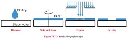
8 All rights reserved. Do not copy or distribute National Technology and Wafer: Thin slice of semiconductor material with highly polished surface Processed wafer is cut into many dies or chips. Lithography: Defining spatial pattern Photoresist: Polymer material that does not allow etching or deposition of areas underneath it. All rights reserved. Do not copy or distribute National Technology and Lithography: Defining spatial pattern Photoresist: Polymer material that does not allow etching or deposition of areas underneath it. 8


9 All rights reserved. Do not copy or distribute National Technology and All rights reserved. Do not copy or distribute National Technology and All rights reserved. Do not copy or distribute National Technology and 9


")
10 Tech Brief 6: Display Technologies Tech Brief 6: Display Technologies Digital Light Processing (DLP) Summary 10
Depletion-mode operation ( 공핍형 ): Using an input gate voltage to effectively decrease the channel size of an FET
: Using an input gate voltage to effectively decrease the channel size of an FET") Ch. 13 MOSFET Metal-Oxide-Semiconductor Field-Effect Transistor : I D D-mode E-mode V g The gate oxide is made of dielectric SiO 2 with e = 3.9 Depletion-mode operation ( 공핍형 ): Using an input gate voltage
Ch. 13 MOSFET Metal-Oxide-Semiconductor Field-Effect Transistor : I D D-mode E-mode V g The gate oxide is made of dielectric SiO 2 with e = 3.9 Depletion-mode operation ( 공핍형 ): Using an input gate voltage
Reading. Lecture 17: MOS transistors digital. Context. Digital techniques:
 Reading Lecture 17: MOS transistors digital Today we are going to look at the analog characteristics of simple digital devices, 5. 5.4 And following the midterm, we will cover PN diodes again in forward
Design cycle for MEMS
 Design cycle for MEMS Design cycle for ICs IC Process Selection nmos CMOS BiCMOS ECL for logic for I/O and driver circuit for critical high speed parts of the system The Real Estate of a Wafer MOS Transistor
ENEE307 Lab 7 MOS Transistors 2: Small Signal Amplifiers and Digital Circuits
 ENEE307 Lab 7 MOS Transistors 2: Small Signal Amplifiers and Digital Circuits In this lab, we will be looking at ac signals with MOSFET circuits and digital electronics. The experiments will be performed
ECE 546 Lecture 12 Integrated Circuits
 ECE 546 Lecture 12 Integrated Circuits Spring 2018 Jose E. Schutt-Aine Electrical & Computer Engineering University of Illinois jesa@illinois.edu ECE 546 Jose Schutt Aine 1 Integrated Circuits IC Requirements
Lecture 11 Circuits numériques (I) L'inverseur
 L'inverseur") Lecture 11 Circuits numériques (I) L'inverseur Outline Introduction to digital circuits The inverter NMOS inverter with resistor pull-up 6.12 Spring 24 Lecture 11 1 1. Introduction to digital circuits:
Lecture 11 Circuits numériques (I) L'inverseur Outline Introduction to digital circuits The inverter NMOS inverter with resistor pull-up 6.12 Spring 24 Lecture 11 1 1. Introduction to digital circuits:
Lecture 13. Biasing and Loading Single Stage FET Amplifiers. The Building Blocks of Analog Circuits - III
 Lecture 3 Biasing and Loading Single Stage FET Amplifiers The Building Blocks of Analog Circuits III In this lecture you will learn: Current biasing of circuits Current sources and sinks for CS, CG, and
Lecture 9 Transistors
 Lecture 9 Transistors Physics Transistor/transistor logic CMOS logic CA 1947 http://www.extremetech.com/extreme/164301-graphenetransistors-based-on-negative-resistance-could-spell-theend-of-silicon-and-semiconductors
EET 438a Automatic Control Systems Technology Laboratory 1 Analog Sensor Signal Conditioning
 EET 438a Automatic Control Systems Technology Laboratory 1 Analog Sensor Signal Conditioning Objectives: Use analog OP AMP circuits to scale the output of a sensor to signal levels commonly found in practical
Lecture 11 Digital Circuits (I) THE INVERTER
 THE INVERTER") Lecture 11 Digital Circuits (I) THE INVERTER Outline Introduction to digital circuits The inverter NMOS inverter with resistor pull-up Reading Assignment: Howe and Sodini; Chapter 5, Sections 5.1-5.3 6.12
Lecture 11 Digital Circuits (I) THE INVERTER Outline Introduction to digital circuits The inverter NMOS inverter with resistor pull-up Reading Assignment: Howe and Sodini; Chapter 5, Sections 5.1-5.3 6.12
ET475 Electronic Circuit Design I [Onsite]
![ET475 Electronic Circuit Design I [Onsite]](/thumbs/89/98281525.jpg "ET475 Electronic Circuit Design I [Onsite]") ET475 Electronic Circuit Design I [Onsite] Course Description: This course covers the analysis and design of electronic circuits, and includes a laboratory that utilizes computer-aided software tools for
ET475 Electronic Circuit Design I [Onsite] Course Description: This course covers the analysis and design of electronic circuits, and includes a laboratory that utilizes computer-aided software tools for
IFB270 Advanced Electronic Circuits
 IFB270 Advanced Electronic Circuits Chapter 9: FET amplifiers and switching circuits Prof. Manar Mohaisen Department of EEC Engineering Review of the Precedent Lecture Review of basic electronic devices
UMAINE ECE Morse Code ROM and Transmitter at ISM Band Frequency
 UMAINE ECE Morse Code ROM and Transmitter at ISM Band Frequency Jamie E. Reinhold December 15, 2011 Abstract The design, simulation and layout of a UMAINE ECE Morse code Read Only Memory and transmitter
Chapter 13: Introduction to Switched- Capacitor Circuits
 Chapter 13: Introduction to Switched- Capacitor Circuits 13.1 General Considerations 13.2 Sampling Switches 13.3 Switched-Capacitor Amplifiers 13.4 Switched-Capacitor Integrator 13.5 Switched-Capacitor
4.2.2 Metal Oxide Semiconductor Field Effect Transistor (MOSFET)
") 4.2.2 Metal Oxide Semiconductor Field Effect Transistor (MOSFET) The Metal Oxide Semitonductor Field Effect Transistor (MOSFET) has two modes of operation, the depletion mode, and the enhancement mode.
4.2.2 Metal Oxide Semiconductor Field Effect Transistor (MOSFET) The Metal Oxide Semitonductor Field Effect Transistor (MOSFET) has two modes of operation, the depletion mode, and the enhancement mode.
Lecture 6: Electronics Beyond the Logic Switches Xufeng Kou School of Information Science and Technology ShanghaiTech University
 Lecture 6: Electronics Beyond the Logic Switches Xufeng Kou School of Information Science and Technology ShanghaiTech University EE 224 Solid State Electronics II Lecture 3: Lattice and symmetry 1 Outline
The Design and Realization of Basic nmos Digital Devices
 Proceedings of The National Conference On Undergraduate Research (NCUR) 2004 Indiana University Purdue University Indianapolis, Indiana April 15-17, 2004 The Design and Realization of Basic nmos Digital
ECE380 Digital Logic. Logic values as voltage levels
 ECE380 Digital Logic Implementation Technology: NMOS and PMOS Transistors, CMOS logic gates Dr. D. J. Jackson Lecture 13-1 Logic values as voltage levels V ss is the minimum voltage that can exist in the
ECE/CoE 0132: FETs and Gates
 ECE/CoE 0132: FETs and Gates Kartik Mohanram September 6, 2017 1 Physical properties of gates Over the next 2 lectures, we will discuss some of the physical characteristics of integrated circuits. We will
Chapter 3-2 Semiconductor devices Transistors and Amplifiers-BJT Department of Mechanical Engineering
 MEMS1082 Chapter 3-2 Semiconductor devices Transistors and Amplifiers-BJT Bipolar Transistor Construction npn BJT Transistor Structure npn BJT I = I + E C I B V V BE CE = V = V B C V V E E Base-to-emitter
Chapter 6 DIFFERENT TYPES OF LOGIC GATES
 Chapter 6 DIFFERENT TYPES OF LOGIC GATES Lesson 8 NMOS gates Ch06L8-"Digital Principles and Design", Raj Kamal, Pearson Education, 2006 2 Outline NMOS (n-channel based MOSFETs based circuit) NMOS Features
Lecture Summary Module 1 Switching Algebra and CMOS Logic Gates
 Lecture Summary Module 1 Switching Algebra and CMOS Logic Gates Learning Outcome: an ability to analyze and design CMOS logic gates Learning Objectives: 1-1. convert numbers from one base (radix) to another:
University of Pittsburgh
 University of Pittsburgh Experiment #7 Lab Report Analog-Digital Applications Submission Date: 08/01/2018 Instructors: Dr. Ahmed Dallal Shangqian Gao Submitted By: Nick Haver & Alex Williams Station #2
Figure 1: JFET common-source amplifier. A v = V ds V gs
 Chapter 7: FET Amplifiers Switching and Circuits The Common-Source Amplifier In a common-source (CS) amplifier, the input signal is applied to the gate and the output signal is taken from the drain. The
DIGITAL VLSI LAB ASSIGNMENT 1
 DIGITAL VLSI LAB ASSIGNMENT 1 Problem 1: NMOS and PMOS plots using Cadence. In this exercise, you are required to generate both NMOS and PMOS I-V device characteristics (I/P and O/P) using Cadence (Use
Approximate Hybrid Equivalent Circuits. Again, the impedance looking into the output terminals is infinite so that. conductance is zero.
 Again, the impedance looking into the output terminals is infinite so that conductance is zero. Hence, the four h-parameters of an ideal transistor connected in CE transistor are The hybrid equivalent
Improved Inverter: Current-Source Pull-Up. MOS Inverter with Current-Source Pull-Up. What else could be connected between the drain and V DD?
 Improved Inverter: Current-Source Pull-Up MOS Inverter with Current-Source Pull-Up What else could be connected between the drain and? Replace resistor with current source I SUP roc i D v IN v OUT Find
Topic 3. CMOS Fabrication Process
 Topic 3 CMOS Fabrication Process Peter Cheung Department of Electrical & Electronic Engineering Imperial College London URL: www.ee.ic.ac.uk/pcheung/ E-mail: p.cheung@ic.ac.uk Lecture 3-1 Layout of a Inverter
ECE520 VLSI Design. Lecture 2: Basic MOS Physics. Payman Zarkesh-Ha
 ECE520 VLSI Design Lecture 2: Basic MOS Physics Payman Zarkesh-Ha Office: ECE Bldg. 230B Office hours: Wednesday 2:00-3:00PM or by appointment E-mail: pzarkesh@unm.edu Slide: 1 Review of Last Lecture Semiconductor
Lecture 01 Operational Amplifiers Op-Amps Introduction
 Lecture 01 Operational Amplifiers Op-Amps Introduction Chapter 9 Ideal Operational Amplifiers and Op-Amp Circuits Donald A. Neamen (2009). Microelectronics: Circuit Analysis and Design, 4th Edition, Mc-Graw-Hill
BJT Amplifier. Superposition principle (linear amplifier)
") BJT Amplifier Two types analysis DC analysis Applied DC voltage source AC analysis Time varying signal source Superposition principle (linear amplifier) The response of a linear amplifier circuit excited
BJT Amplifier Two types analysis DC analysis Applied DC voltage source AC analysis Time varying signal source Superposition principle (linear amplifier) The response of a linear amplifier circuit excited
ECE 334: Electronic Circuits Lecture 10: Digital CMOS Circuits
 Faculty of Engineering ECE 334: Electronic Circuits Lecture 10: Digital CMOS Circuits CMOS Technology Complementary MOS, or CMOS, needs both PMOS and NMOS FET devices for their logic gates to be realized
EE 330 Laboratory 7 MOSFET Device Experimental Characterization and Basic Applications Spring 2017
 EE 330 Laboratory 7 MOSFET Device Experimental Characterization and Basic Applications Spring 2017 Objective: The objective of this laboratory experiment is to become more familiar with the operation of
Digital Electronics Part II - Circuits
 Digital Electronics Part II - Circuits Dr. I. J. Wassell Gates from Transistors 1 Introduction Logic circuits are non-linear, consequently we will introduce a graphical technique for analysing such circuits
Student Lecture by: Giangiacomo Groppi Joel Cassell Pierre Berthelot September 28 th 2004
 Student Lecture by: Giangiacomo Groppi Joel Cassell Pierre Berthelot September 28 th 2004 Lecture outline Historical introduction Semiconductor devices overview Bipolar Junction Transistor (BJT) Field
Layout of a Inverter. Topic 3. CMOS Fabrication Process. The CMOS Process - photolithography (2) The CMOS Process - photolithography (1) v o.
 The CMOS Process - photolithography (1) v o.") Layout of a Inverter Topic 3 CMOS Fabrication Process V DD Q p Peter Cheung Department of Electrical & Electronic Engineering Imperial College London v i v o Q n URL: www.ee.ic.ac.uk/pcheung/ E-mail: p.cheung@ic.ac.uk
Layout of a Inverter Topic 3 CMOS Fabrication Process V DD Q p Peter Cheung Department of Electrical & Electronic Engineering Imperial College London v i v o Q n URL: www.ee.ic.ac.uk/pcheung/ E-mail: p.cheung@ic.ac.uk
UNIT-VI FIELD EFFECT TRANSISTOR. 1. Explain about the Field Effect Transistor and also mention types of FET s.
 UNIT-I FIELD EFFECT TRANSISTOR 1. Explain about the Field Effect Transistor and also mention types of FET s. The Field Effect Transistor, or simply FET however, uses the voltage that is applied to their
Lecture Week 5. Quiz #2 Ohm s Law Homework Power Review Shorthand Notation Active Components Ideal Op-amps
 Lecture Week 5 Quiz #2 Ohm s Law Homework Power Review Shorthand Notation Active Components Ideal Op-amps Quiz 2 Ohm s Law (20 pts.) Please clear desks and turn off phones and put them in back packs You
Field Effect Transistors (npn)
") Field Effect Transistors (npn) gate drain source FET 3 terminal device channel e - current from source to drain controlled by the electric field generated by the gate base collector emitter BJT 3 terminal
Field Effect Transistors (npn) gate drain source FET 3 terminal device channel e - current from source to drain controlled by the electric field generated by the gate base collector emitter BJT 3 terminal
TECHNO INDIA BATANAGAR (DEPARTMENT OF ELECTRONICS & COMMUNICATION ENGINEERING) QUESTION BANK- 2018
 QUESTION BANK- 2018") TECHNO INDIA BATANAGAR (DEPARTMENT OF ELECTRONICS & COMMUNICATION ENGINEERING) QUESTION BANK- 2018 Paper Setter Detail Name Designation Mobile No. E-mail ID Raina Modak Assistant Professor 6290025725 raina.modak@tib.edu.in
TECHNO INDIA BATANAGAR (DEPARTMENT OF ELECTRONICS & COMMUNICATION ENGINEERING) QUESTION BANK- 2018 Paper Setter Detail Name Designation Mobile No. E-mail ID Raina Modak Assistant Professor 6290025725 raina.modak@tib.edu.in
Memory Basics. historically defined as memory array with individual bit access refers to memory with both Read and Write capabilities
 Memory Basics RAM: Random Access Memory historically defined as memory array with individual bit access refers to memory with both Read and Write capabilities ROM: Read Only Memory no capabilities for
Homework KCL/KVL Review Bode Plots Active Filters
 Homework KCL/KVL Review Bode Plots Active Filters Homeworkdue 3/6 (Najera), due 3/9 (Quinones) SUCCESS POINTS: REPORT WRITING CHECK TO MAKE SURE EVERYTHING YOU SAY REFER DIRECTLY TO YOUR TABLES AND GRAPHS?
C H A P T E R 5. Amplifier Design
 C H A P T E 5 Amplifier Design The Common-Source Amplifier v 0 = r ( g mvgs )( D 0 ) A v0 = g m r ( D 0 ) Performing the analysis directly on the circuit diagram with the MOSFET model used implicitly.
Carleton University. Faculty of Engineering and Design, Department of Electronics. ELEC 2507 Electronic - I Summer Term 2017
 Carleton University Faculty of Engineering and Design, Department of Electronics Instructors: ELEC 2507 Electronic - I Summer Term 2017 Name Section Office Email Prof. Q. J. Zhang Section A 4148 ME qjz@doe.carleton.ca
INTRODUCTION TO ELECTRONICS EHB 222E
 INTRODUCTION TO ELECTRONICS EHB 222E MOS Field Effect Transistors (MOSFETS II) MOSFETS 1/ INTRODUCTION TO ELECTRONICS 1 MOSFETS Amplifiers Cut off when v GS < V t v DS decreases starting point A, once
Logic diagram: a graphical representation of a circuit
 LOGIC AND GATES Introduction to Logic (1) Logic diagram: a graphical representation of a circuit Each type of gate is represented by a specific graphical symbol Truth table: defines the function of a gate
ECE 340 Lecture 40 : MOSFET I
 ECE 340 Lecture 40 : MOSFET I Class Outline: MOS Capacitance-Voltage Analysis MOSFET - Output Characteristics MOSFET - Transfer Characteristics Things you should know when you leave Key Questions How do
USER MANUAL FOR THE LM2901 QUAD VOLTAGE COMPARATOR FUNCTIONAL MODULE
 USER MANUAL FOR THE LM2901 QUAD VOLTAGE COMPARATOR FUNCTIONAL MODULE LM2901 Quad Voltage Comparator 1 5/18/04 TABLE OF CONTENTS 1. Index of Figures....3 2. Index of Tables. 3 3. Introduction.. 4-5 4. Theory
Digital Electronics. Assign 1 and 0 to a range of voltage (or current), with a separation that minimizes a transition region. Positive Logic.
, with a separation that minimizes a transition region. Positive Logic.") Digital Electronics Assign 1 and 0 to a range of voltage (or current), with a separation that minimizes a transition region Positive Logic Logic 1 Negative Logic Logic 0 Voltage Transition Region Transition
Digital Electronics Assign 1 and 0 to a range of voltage (or current), with a separation that minimizes a transition region Positive Logic Logic 1 Negative Logic Logic 0 Voltage Transition Region Transition
420 Intro to VLSI Design
 Dept of Electrical and Computer Engineering 420 Intro to VLSI Design Lecture 0: Course Introduction and Overview Valencia M. Joyner Spring 2005 Getting Started Syllabus About the Instructor Labs, Problem
ECE 2300 Digital Logic & Computer Organization
 ECE 2300 Digital Logic & Computer Organization Spring 2018 CMOS Logic Lecture 4: 1 NAND Logic Gate X Y (X Y) = NAND Using De Morgan s Law: (X Y) = X +Y X X X +Y = Y Y Also a NAND We can build circuits
INTRODUCTION TO MOS TECHNOLOGY
 INTRODUCTION TO MOS TECHNOLOGY 1. The MOS transistor The most basic element in the design of a large scale integrated circuit is the transistor. For the processes we will discuss, the type of transistor
Gates and Circuits 1
 1 Gates and Circuits Chapter Goals Identify the basic gates and describe the behavior of each Describe how gates are implemented using transistors Combine basic gates into circuits Describe the behavior
Lecture 12 - Digital Circuits (I) The inverter. October 20, 2005
 The inverter. October 20, 2005") 6.12 - Microelectronic Devices and Circuits - Fall 25 Lecture 12-1 Lecture 12 - Digital Circuits (I) The inverter October 2, 25 Contents: 1. Introduction to digital electronics: the inverter 2. NMOS inverter
6.12 - Microelectronic Devices and Circuits - Fall 25 Lecture 12-1 Lecture 12 - Digital Circuits (I) The inverter October 2, 25 Contents: 1. Introduction to digital electronics: the inverter 2. NMOS inverter
Introduction to MOSFET MOSFET (Metal Oxide Semiconductor Field Effect Transistor)
") Microelectronic Circuits Introduction to MOSFET MOSFET (Metal Oxide Semiconductor Field Effect Transistor) Slide 1 MOSFET Construction MOSFET (Metal Oxide Semiconductor Field Effect Transistor) Slide 2
Microelectronic Circuits Introduction to MOSFET MOSFET (Metal Oxide Semiconductor Field Effect Transistor) Slide 1 MOSFET Construction MOSFET (Metal Oxide Semiconductor Field Effect Transistor) Slide 2
ELEC 350L Electronics I Laboratory Fall 2012
 ELEC 350L Electronics I Laboratory Fall 2012 Lab #9: NMOS and CMOS Inverter Circuits Introduction The inverter, or NOT gate, is the fundamental building block of most digital devices. The circuits used
Q1. Explain the construction and principle of operation of N-Channel and P-Channel Junction Field Effect Transistor (JFET).
.") Q. Explain the construction and principle of operation of N-Channel and P-Channel Junction Field Effect Transistor (JFET). Answer: N-Channel Junction Field Effect Transistor (JFET) Construction: Drain(D)
Q. Explain the construction and principle of operation of N-Channel and P-Channel Junction Field Effect Transistor (JFET). Answer: N-Channel Junction Field Effect Transistor (JFET) Construction: Drain(D)
Module-3: Metal Oxide Semiconductor (MOS) & Emitter coupled logic (ECL) families
 & Emitter coupled logic (ECL) families") 1 Module-3: Metal Oxide Semiconductor (MOS) & Emitter coupled logic (ECL) families 1. Introduction 2. Metal Oxide Semiconductor (MOS) logic 2.1. Enhancement and depletion mode 2.2. NMOS and PMOS inverter
1 Module-3: Metal Oxide Semiconductor (MOS) & Emitter coupled logic (ECL) families 1. Introduction 2. Metal Oxide Semiconductor (MOS) logic 2.1. Enhancement and depletion mode 2.2. NMOS and PMOS inverter
IENGINEERS-CONSULTANTS QUESTION BANK SERIES ELECTRONICS ENGINEERING 1 YEAR UPTU ELECTRONICS ENGINEERING EC 101 UNIT 3 (JFET AND MOSFET)
") ELECTRONICS ENGINEERING EC 101 UNIT 3 (JFET AND MOSFET) LONG QUESTIONS (10 MARKS) 1. Draw the construction diagram and explain the working of P-Channel JFET. Also draw the characteristics curve and transfer
ELECTRONICS ENGINEERING EC 101 UNIT 3 (JFET AND MOSFET) LONG QUESTIONS (10 MARKS) 1. Draw the construction diagram and explain the working of P-Channel JFET. Also draw the characteristics curve and transfer
Designing Information Devices and Systems II Fall 2017 Note 1
 EECS 16B Designing Information Devices and Systems II Fall 2017 Note 1 1 Digital Information Processing Electrical circuits manipulate voltages (V ) and currents (I) in order to: 1. Process information
(a) Current-controlled and (b) voltage-controlled amplifiers.
 Current-controlled and (b) voltage-controlled amplifiers.") Fig. 6.1 (a) Current-controlled and (b) voltage-controlled amplifiers. Fig. 6.2 Drs. Ian Munro Ross (front) and G. C. Dacey jointly developed an experimental procedure for measuring the characteristics
Fig. 6.1 (a) Current-controlled and (b) voltage-controlled amplifiers. Fig. 6.2 Drs. Ian Munro Ross (front) and G. C. Dacey jointly developed an experimental procedure for measuring the characteristics
MOSFET Amplifier Design Project Electrical Engineering 310 Section 002 Shawn Moser
 MOSFET Amplifier Design Project Electrical Engineering 0 Section 00 Shawn Moser Introduction: In this lab, my partner and I were tasked with the construction of a linear electronic circuit that functions
Logic signal voltage levels
 Logic signal voltage levels Logic gate circuits are designed to input and output only two types of signals: "high" (1) and "low" (0), as represented by a variable voltage: full power supply voltage for
Common Reference Example
 Operational Amplifiers Overview Common reference circuit diagrams Real models of operational amplifiers Ideal models operational amplifiers Inverting amplifiers Noninverting amplifiers Summing amplifiers
Field Effect Transistors
 Field Effect Transistors Purpose In this experiment we introduce field effect transistors (FETs). We will measure the output characteristics of a FET, and then construct a common-source amplifier stage,
ECE 5745 Complex Digital ASIC Design Topic 2: CMOS Devices
 ECE 5745 Complex Digital ASIC Design Topic 2: CMOS Devices Christopher Batten School of Electrical and Computer Engineering Cornell University http://www.csl.cornell.edu/courses/ece5950 Simple Transistor
In this lecture we will begin a new topic namely the Metal-Oxide-Semiconductor Field Effect Transistor.
 Solid State Devices Dr. S. Karmalkar Department of Electronics and Communication Engineering Indian Institute of Technology, Madras Lecture - 38 MOS Field Effect Transistor In this lecture we will begin
Lecture 0: Introduction
 Lecture 0: Introduction Introduction Integrated circuits: many transistors on one chip. Very Large Scale Integration (VLSI): bucketloads! Complementary Metal Oxide Semiconductor Fast, cheap, low power
Section 4: Operational Amplifiers
 Section 4: Operational Amplifiers Op Amps Integrated circuits Simpler to understand than transistors Get back to linear systems, but now with gain Come in various forms Comparators Full Op Amps Differential
ECE 340 Lecture 37 : Metal- Insulator-Semiconductor FET Class Outline:
 ECE 340 Lecture 37 : Metal- Insulator-Semiconductor FET Class Outline: Metal-Semiconductor Junctions MOSFET Basic Operation MOS Capacitor Things you should know when you leave Key Questions What is the
Analog I/O. ECE 153B Sensor & Peripheral Interface Design Winter 2016
 Analog I/O ECE 153B Sensor & Peripheral Interface Design Introduction Anytime we need to monitor or control analog signals with a digital system, we require analogto-digital (ADC) and digital-to-analog
hij Teacher Resource Bank GCE Electronics Exemplar Examination Questions ELEC2 Further Electronics
 hij Teacher Resource Bank GCE Electronics Exemplar Examination Questions ELEC2 Further Electronics The Assessment and Qualifications Alliance (AQA) is a company limited by guarantee registered in England
Designing of a 8-bits DAC in 0.35µm CMOS Technology For High Speed Communication Systems Application
 Designing of a 8-bits DAC in 035µm CMOS Technology For High Speed Communication Systems Application Veronica Ernita Kristianti, Hamzah Afandi, Eri Prasetyo ibowo, Brahmantyo Heruseto and shinta Kisriani
Emitter Coupled Differential Amplifier
 Emitter Coupled Differential Amplifier Returning to the transistor, a very common and useful circuit is the differential amplifier. It's basic circuit is: Vcc Q1 Q2 Re Vee To see how this circuit works,
Chapter 2 : Semiconductor Materials & Devices (II) Feb
 Feb") Chapter 2 : Semiconductor Materials & Devices (II) 1 Reference 1. SemiconductorManufacturing Technology: Michael Quirk and Julian Serda (2001) 3. Microelectronic Circuits (5/e): Sedra & Smith (2004) 4.
Chapter 2 : Semiconductor Materials & Devices (II) 1 Reference 1. SemiconductorManufacturing Technology: Michael Quirk and Julian Serda (2001) 3. Microelectronic Circuits (5/e): Sedra & Smith (2004) 4.
CENG4480 Lecture 04: Analog/Digital Conversions
 CENG4480 Lecture 04: Analog/Digital Conversions Bei Yu byu@cse.cuhk.edu.hk (Latest update: October 3, 2018) Fall 2018 1 / 31 Overview Preliminaries Comparator Digital to Analog Conversion (DAC) Analog
Chapter 6 DIFFERENT TYPES OF LOGIC GATES
 Chapter 6 DIFFERENT TYPES OF LOGIC GATES Lesson 9 CMOS gates Ch06L9-"Digital Principles and Design", Raj Kamal, Pearson Education, 2006 2 Outline CMOS (n-channel based MOSFETs based circuit) CMOS Features
EE 230 Lab Lab 9. Prior to Lab
 MOS transistor characteristics This week we look at some MOS transistor characteristics and circuits. Most of the measurements will be done with our usual lab equipment, but we will also use the parameter
Chapter 2. Operational Amplifiers
 Chapter 2. Operational Amplifiers Tong In Oh 1 Objective Terminal characteristics of the ideal op amp How to analyze op amp circuits How to use op amps to design amplifiers How to design more sophisticated
Notes. (Subject Code: 7EC5)
") COMPUCOM INSTITUTE OF TECHNOLOGY & MANAGEMENT, JAIPUR (DEPARTMENT OF ELECTRONICS & COMMUNICATION) Notes VLSI DESIGN NOTES (Subject Code: 7EC5) Prepared By: MANVENDRA SINGH Class: B. Tech. IV Year, VII
COMPUCOM INSTITUTE OF TECHNOLOGY & MANAGEMENT, JAIPUR (DEPARTMENT OF ELECTRONICS & COMMUNICATION) Notes VLSI DESIGN NOTES (Subject Code: 7EC5) Prepared By: MANVENDRA SINGH Class: B. Tech. IV Year, VII
Shorthand Notation for NMOS and PMOS Transistors
 Shorthand Notation for NMOS and PMOS Transistors Terminal Voltages Mode of operation depends on V g, V d, V s V gs = V g V s V gd = V g V d V ds = V d V s = V gs - V gd Source and drain are symmetric diffusion
Semiconductor Physics and Devices
 Metal-Semiconductor and Semiconductor Heterojunctions The Metal-Oxide-Semiconductor Field-Effect Transistor (MOSFET) is one of two major types of transistors. The MOSFET is used in digital circuit, because
Device Technology( Part 2 ): CMOS IC Technologies
: CMOS IC Technologies") 1 Device Technology( Part 2 ): CMOS IC Technologies Chapter 3 : Semiconductor Manufacturing Technology by M. Quirk & J. Serda Saroj Kumar Patra, Department of Electronics and Telecommunication, Norwegian
1 Device Technology( Part 2 ): CMOS IC Technologies Chapter 3 : Semiconductor Manufacturing Technology by M. Quirk & J. Serda Saroj Kumar Patra, Department of Electronics and Telecommunication, Norwegian
Federal Urdu University of Arts, Science & Technology Islamabad Pakistan THIRD SEMESTER ELECTRONICS - II BASIC ELECTRICAL & ELECTRONICS LAB
 THIRD SEMESTER ELECTRONICS - II BASIC ELECTRICAL & ELECTRONICS LAB DEPARTMENT OF ELECTRICAL ENGINEERING Prepared By: Checked By: Approved By: Engr. Saqib Riaz Engr. M.Nasim Khan Dr.Noman Jafri Lecturer
Basic Electronics. Introductory Lecture Course for. Technology and Instrumentation in Particle Physics Chicago, Illinois June 9-14, 2011
 Basic Electronics Introductory Lecture Course for Technology and Instrumentation in Particle Physics 2011 Chicago, Illinois June 9-14, 2011 Presented By Gary Drake Argonne National Laboratory Session 3
EECS130 Integrated Circuit Devices
 EECS130 Integrated Circuit Devices Professor Ali Javey 11/6/2007 MOSFETs Lecture 6 BJTs- Lecture 1 Reading Assignment: Chapter 10 More Scalable Device Structures Vertical Scaling is important. For example,
CMOS Technology. 1. Why CMOS 2. Qualitative MOSFET model 3. Building a MOSFET 4. CMOS logic gates. Handouts: Lecture Slides. metal ndiff.
 CMOS Technology 1. Why CMOS 2. Qualitative MOSFET model 3. Building a MOSFET 4. CMOS logic gates poly pdiff metal ndiff Handouts: Lecture Slides L03 - CMOS Technology 1 Building Bits from Atoms V in V
Metal-Oxide-Silicon (MOS) devices PMOS. n-type
 devices PMOS. n-type") Metal-Oxide-Silicon (MOS devices Principle of MOS Field Effect Transistor transistor operation Metal (poly gate on oxide between source and drain Source and drain implants of opposite type to substrate.
Metal-Oxide-Silicon (MOS devices Principle of MOS Field Effect Transistor transistor operation Metal (poly gate on oxide between source and drain Source and drain implants of opposite type to substrate.
Electronic Circuits for Mechatronics ELCT 609 Lecture 7: MOS-FET Amplifiers
 Electronic Circuits for Mechatronics ELCT 609 Lecture 7: MOS-FET Amplifiers Assistant Professor Office: C3.315 E-mail: eman.azab@guc.edu.eg 1 Enhancement N-MOS Modes of Operation Mode V GS I DS V DS Cutoff
Analog Electronics. Electronic Devices, 9th edition Thomas L. Floyd Pearson Education. Upper Saddle River, NJ, All rights reserved.
 Analog Electronics BJT Structure The BJT has three regions called the emitter, base, and collector. Between the regions are junctions as indicated. The base is a thin lightly doped region compared to the
Lesson number one. Operational Amplifier Basics
 What About Lesson number one Operational Amplifier Basics As well as resistors and capacitors, Operational Amplifiers, or Op-amps as they are more commonly called, are one of the basic building blocks
EE 330 Laboratory 8 Discrete Semiconductor Amplifiers
 EE 330 Laboratory 8 Discrete Semiconductor Amplifiers Fall 2017 Contents Objective:... 2 Discussion:... 2 Components Needed:... 2 Part 1 Voltage Controlled Amplifier... 2 Part 2 Common Source Amplifier...
8. Combinational MOS Logic Circuits
 8. Combinational MOS Introduction Combinational logic circuits, or gates, witch perform Boolean operations on multiple input variables and determine the output as Boolean functions of the inputs, are the
6.111 Lecture # 15. Operational Amplifiers. Uses of Op Amps
 6.111 Lecture # 15 Operational Amplifiers Parameter Ideal '741 '357 Int Gain A Infinity 200,000/f(Hz) 20x10^6/f(Hz) Uses of Op Amps Analog uses employ negative feedback to drive + input to (nearly) the
ANALOG FUNDAMENTALS C. Topic 4 BASIC FET AMPLIFIER CONFIGURATIONS
 AV18-AFC ANALOG FUNDAMENTALS C Topic 4 BASIC FET AMPLIFIER CONFIGURATIONS 1 ANALOG FUNDAMENTALS C AV18-AFC Overview This topic identifies the basic FET amplifier configurations and their principles of
Fig 1: The symbol for a comparator
 INTRODUCTION A comparator is a device that compares two voltages or currents and switches its output to indicate which is larger. They are commonly used in devices such as They are commonly used in devices
CHAPTER 7 HARDWARE IMPLEMENTATION
 168 CHAPTER 7 HARDWARE IMPLEMENTATION 7.1 OVERVIEW In the previous chapters discussed about the design and simulation of Discrete controller for ZVS Buck, Interleaved Boost, Buck-Boost, Double Frequency
Gechstudentszone.wordpress.com
 UNIT 4: Small Signal Analysis of Amplifiers 4.1 Basic FET Amplifiers In the last chapter, we described the operation of the FET, in particular the MOSFET, and analyzed and designed the dc response of circuits
EE 5611 Introduction to Microelectronic Technologies Fall Thursday, September 04, 2014 Lecture 02
 EE 5611 Introduction to Microelectronic Technologies Fall 2014 Thursday, September 04, 2014 Lecture 02 1 Lecture Outline Review on semiconductor materials Review on microelectronic devices Example of microelectronic
EEC 216 Lecture #10: Ultra Low Voltage and Subthreshold Circuit Design. Rajeevan Amirtharajah University of California, Davis
 EEC 216 Lecture #1: Ultra Low Voltage and Subthreshold Circuit Design Rajeevan Amirtharajah University of California, Davis Opportunities for Ultra Low Voltage Battery Operated and Mobile Systems Wireless