INTRODUCTION. Magnetics
|
|
|
- Julius Ellis
- 5 years ago
- Views:
Transcription
1 M GNETICS
2
3 INTRODUCTION Magnetics From overcurrent and overvoltage protection to supercapacitors and magnetics, Cooper Bussmann provides integrated solutions that meet the evolving needs of technology-driven markets. Cooper Bussmann is a leader and an innovator in providing cost-effective, comprehensive solutions that utilize the high quality brand names that customers know and trust. Overcurrent The Bussmann Electronic Fuse family offers fail-safe circuit protection devices in SMD, Thru-Hole, and traditional Ferrule Fuse packages. Magnetics The Coiltronics family of transformers and inductors offers a broad range of solutions to meet precise specifications in a variety of applications. Overvoltage The PolySURG family offers protection for sensitive electronic circuits from the damaging effects of electrostatic discharge (ESD). Supercapacitors The PowerStor family of aerogel capacitors offers ultra-low resistance supercapacitors, unique high-energy storage devices. Cooper Bussmann continues its 9-year history of blazing new trails of innovative technologies. Cooper Bussmann manufactures the industry s first truly global product line. Each item is backed by an efficient worldwide network of distribution, customer service and technical support. Bussmann products include the most extensive circuit protection solutions approved for use in compliance with a variety of major standards: UL, CS, IEC within wide range of applications: industrial motor protection, power conversion, medium voltage, power distribution, telecommunications network equipment, electronics, and automotive. Manufacturing operations in North merica, Europe, and sia have earned ISO 9 certification. Bussmann customers are assured of only the utmost quality across every product line. Our team is knowledgeable, responsive and customer focused. Bussmann continues to set the standard for circuit protection solutions around the world. To receive further information on Cooper Bussmann products, visit or contact customer service at PM-

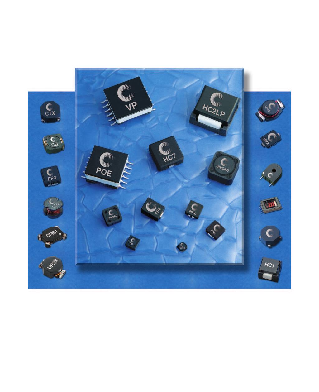
4 Power Magnetics G r o u p Leading-Edge Technology leading global brand name in the power magnetics marketplace since 977. Coiltronics brand magnetics specializes in standard and custom solutions offering the latest in state-of-the-art low profile high power density magnetic components. In working closely with the industry leaders in chipset and core development, we remain at the forefront of innovation and new technology to deliver the optimal mix of packaging, high efficiency and unbeatable reliability. Our designs utilize high frequency, low core loss materials, new and custom core shapes in combination with innovative construction and packaging to provide designers with the highest performance parts available on the market. RoHS /95/EC Market-Driven Products Coiltronics brand magnetics is the first choice in power inductor and transformer solutions to the ever-changing Digital Home, Office and Mobile electronics world. In support of this market, we specialize in inductors and transformers for DC-DC power conversion and switch-mode applications requiring high frequency. Our component solutions can be found in many products requiring power conversion including cellular telephones, digital cameras, MP3 players, notebook and desktop computers & peripherals & LCD displays across the Consumer, Communication, Computer, Industrial and utomotive markets. Standard Products Coiltronics brand product line of power magnetics continually expands to satisfy shifts in technology and related market needs. Categories of Standard Products include: Shielded Drum Inductors Unshielded Drum Inductors High Current Inductors Toroidal Inductors Specialty Magnetics Custom Magnetics Custom-Engineered Capabilities Inductors and Transformers for DC/DC Converters and Off-Line Switch Mode Power Supplies (To Watts at voltages up to 45Vac [64 Vdc] and Frequencies from Khz to Mhz) Custom SMT Inductors and Transformers Coiltronics brand products can provide you with custom designs from print through manufacture. Our design Engineers can take your designated specifications or help you determine what the specifications should be. Either way, we ll get you the right power magnetic solution to your design challenge. PM-

5 Shielded Drum Inductors Coiltronics brand magnetics put forward one of the largest variety of shielded drum core inductors that utilize a magnetic shield reducing EMI effects and have the best power density versus size ratio on the market. Features: Large variety of shapes and sizes Ultra Low Profile (as low as.mm in height) Maximum Power Density Dual Winding: Coupled Inductor, SEPIC, Flyback Transformer, : Isolation Transformer High current Magnetic Shielding, Reduced EMI Compact Footprint Standard Product Families: DR, DRQ, SD, SDQ, SD5, SD38, CD High Current Inductors The Coiltronics brand high current inductor product lines provide an optimal mix of innovative packaging, high efficiency and unbeatable reliability. Features: Large variety of shapes and sizes Low profile (as low as 3mm) Low DCR, High Efficiency Designed for High Current, Low Voltage pplications Foil construction adds higher reliability factor than traditional magnet wire used for higher frequency circuits Gapped Ferrite: Maximum Efficiency, Low core loss High Temperature Powder Iron: 55 C Maximum Temperature Operation, Organic Binder Eliminates Thermal ging Standard Product Families: HC, HCLP, HC3, HC7, HC8, HC8LP, FLT-PC (FP), FLT-PC (FP3), FLT-PC 4 (FP4). Unshielded Drum Core Inductors Coiltronics brand magnetics offer a wide variety of unshielded drum core inductors in different shapes and sizes to fit all board space constraints. Features: Multiple sizes available Miniature Surface Mount Design Low Profile Small Footprint Ferrite Core Material Standard Product Families: UNI-PC (UPB, B, 3B, 4B), UNI-PC.4C (UP.4C), UNI-PC.8B (UP.8B), UNI-PC C (UPC), LD. Toroid Inductors The Coiltronics brand magnetics also offer a mixture of toroid constructed inductors available in surface mount, through hole, and dual winding platforms. Features: Surface Mount and Through-Hole Mounting Maximum Power Density Dual Winding: Coupled Inductor, SEPIC, Flyback Transformer, : Isolation Transformer Low EMI Variety Of Core Materials: Powder Iron, MPP, Gapped Ferrite, morphous Standard Product Families: ECONO-PC, OCT-PC, OCT-PC Plus, MICRO-PC, MICRO-PC Plus, Low Cost Power Inductors (LCPI). Specialty Magnetics Coiltronics brand magnetics also offer a series of specialty magnetics that increase versatility in design needs. Features: Multi-configurable transformer/inductors Variety Of Sizes Multi-configurable Power Over Ethernet/PD Flyback Transformers Current Sense Inductors Cold Cathode Fluorescent Lamp (CCFL) Transformers Common Mode Inductors Surface Mount and Though-Hole Standard Product Families: VERS-PC (VP), VERS-PC High Inductance (VPH), Power Over Ethernet/ PD Configurable Transformer (PoE), Cold Cathode Fluorescent Lamp (CCFL), Common Mode Inductor SMT (CMS), Common Mode Inductor THT (CMT), Current Sense Inductor (CS). Custom Magnetics Coiltronics brand magnetics can be customized to meet your application needs. We specialize in designing product to specific requirements and new technology, as well as modifying our standard product platforms to meet your requirements. Modifications to standard products are available. ll surface mount components are available in tape-and-reel packaging for pick-and-place utilization. PM-3
6 NOTES Magnetics PM-4
7 Table of Contents Inductor Selection Guide Page PM- UNI-PC.8 Low Cost, Low Profile.8mm Power Inductors (Surface Mount) Page PM- UNI-PC.4C Low Cost, Low Profile Power Inductors (Surface Mount) Page PM-4 UNI-PC C Low Cost Power Inductors (Surface Mount) Page PM-5 UNI-PC Power Inductors (Surface Mount) Page PM-7 LD Series Metalized Drum Core Power Inductor Page PM-3 CD Series High Power Density, Low Profile, Shielded Inductors Page PM-6 DR Series High Power Density, High Efficiency, Shielded Inductors Page PM-8 PM-5

8 Table of Contents DRQ Series Dual Winding, Shielded Inductors/Transformer Page PM-33 SD Series High Power Density, Low Profile, Shielded Inductors Page PM-4 SD5 Series High Power Density, Low Profile, Shielded Inductors Page PM-47 SDQ Series Low Profile Dual Winding Shielded Inductor/Transformer Page PM-5 SD38 Series Low Profile, Shielded Inductors Page PM-53 MICRO-PC Low Profile Power Inductors (Surface Mount) Page PM-56 MICRO-PC PLUS Low Profile Power Inductors (Surface Mount) Page PM-57 PM-6
9 Table of Contents ECONO-PC /OCT-PC OCT-PC PLUS Power Inductors and Transformers Page PM-59 FLT-PC Low Profile Inductors (Surface Mount) Page PM-67 FLT-PC 3 Low Profile Inductors Page PM-7 FLT-PC 4 5mm Height Inductors (Surface Mount) Page PM-7 HIGH CURRENT Power Inductors Page PM-75 HIGH CURRENT LP Low Profile Power Inductors Page PM-78 HC3 Series HIGH CURRENT 3 Power Inductors Page PM-8 PM-7
 Page PM-89")
 Page PM- STNDRD GEOMETRIES Low Cost Magnetic Components Page")
10 Table of Contents HC7 Series HIGH CURRENT 7 Power Inductors Page PM-8 HC8LP Series Power Inductors Page PM-84 HC8 Series HIGH CURRENT 8 Power Inductors Page PM-87 VERS-PC Inductors and Transformers (Surface Mount) Page PM-89 Power Over Ethernet (PoE)/PD Configurable Transformer Page PM-97 CCFL TRNSFORMERS Cold Cathode Fluorescent Lamp Inverter Transformers (Through-Hole and Surface Mount) Page PM- STNDRD GEOMETRIES Low Cost Magnetic Components Page PM-3 PM-8

11 Table of Contents CMS-SERIES Common Mode Inductors (Surface Mount) Page PM-8 CMT-SERIES Common Mode Inductors (Through-Hole) Page PM- CS Series Current Sense Current Sense Inductors Page PM-6 LOW COST POWER INDUCTORS Toroidal Inductors Page PM-7 pplication Notes Solder Reflow Profile Using the Versa-Pac as a Flyback Transformer Using the Versa-Pac as a Forward Converter Transformer Power Inductors Improve Reliability in High Temperature Designs Switching Regulator Inductor Design Inductor Selection for SEPIC Designs PoE Power Magnetics - Options and Trends High Current Inductors for DC-DC Converters Magnetics Design Specification Form Page PM- Page PM- Page PM-5 Page PM-8 Page PM-3 Page PM-3 Page PM-34 Page PM-36 Page PM-37 This bulletin is intended to present product design solutions and technical information that will help the end user with design applications. Cooper Electronic Technologies reserves the right, without notice, to change design or construction of any products and to discontinue or limit distribution of any products. Cooper Electronic Technologies also reserves the right to change or update, without notice, any technical information contained in this bulletin. Once a product has been selected, it should be tested by the user in all possible applications. Life Support Policy: Cooper Electronic Technologies does not authorize the use of any of its products for use in life support devices or systems without the express written approval of an officer of the Company. Life support systems are devices which support or sustain life, and whose failure to perform, when properly used in accordance with instructions for use provided in the labeling, can be reasonably expected to result in significant injury to the user. PM-9
12 INDUCTOR SELECTION GUIDE High Current Shielded Drum Drum Core Inductor Selection Guide Maximum Maximum Winding Product Family Current Rating Inductance Rating Configuration Product Size (mm) Core EMI Inductance Current Inductance Current (if applicable) L W H Structure Rating SMT/THT HC UI SMT HC LP UI SMT HC EI SMT HC UI SMT HC7 (HC7-R) EI SMT HC EI SMT HC8LP EI SMT FLT-PC Single (FP4-S_) UI SMT FLT-PC 5mm (FP-V_) UI SMT FLT-PC Single (FP3-S) EI SMT FLT-PC Single (FP-S_) UI SMT FLT-PC Dual (FP-D_) Series UI SMT FLT-PC Dual (FP-D_) Parallel UI SMT DRQ Series Shld Drum SMT DRQ Parallel Shld Drum SMT DR Shld Drum SMT DRQ Parallel Shld Drum SMT DR Shld Drum SMT DRQ Series Shld Drum SMT CD Shld Drum SMT DRQ Series Shld Drum SMT DRQ Parallel Shld Drum SMT DR Shld Drum SMT DRQ Series Shld Drum SMT DRQ Parallel Shld Drum SMT DR Shld Drum SMT SDQ Parallel Shld Drum SMT SDQ Series Shld Drum SMT SD Shld Drum SMT SD Shld Drum SMT SD Shld Drum SMT SD Shld Drum SMT SDQ Series Shld Drum SMT SDQ Parallel Shld Drum SMT SD Shld Drum SMT SD Shld Drum SMT SD Shld Drum SMT SD Shld Drum SMT SD Shld Drum SMT UNI-PC 4B Drum 3 SMT UNI-PC 3B (UP3B) Drum 3 SMT UNI-PC C (UPC) Drum 3 SMT LD Drum 3 SMT UNI-PC B (UPB) Drum 3 SMT UNI-PC.8B (UP.8B) Drum 3 SMT UNI-PC B (UPB) Drum 3 SMT LD Drum 3 SMT UNI-PC.4C (UP.4C) Drum 3 SMT Note = Current ratings listed are the lower value of the Isat and Irms ratings Note = EMI Rating: ) Closed magnetic path - best EMI shield; ) Small gap, or external shield - some EMI fringing; 3) No shield - Highest EMI Note 3 = lternate sizes, terminal styles available PM- General information needed to select proper inductor: I. Inductance and Current requirements II. Mounting style (surface mount or thru hole) and size constraints III. Frequency of operation (switching frequency) IV. Circuit susceptibility to EMI V. Consider using two parts in series for lower profiles, higher current ratings or higher inductance values
13 Toroid Specialty Inductor Selection Guide Maximum Maximum Winding Product Family Current Rating Inductance Rating Configuration Product Size (mm) Core EMI Inductance Current Inductance Current (if applicable) L W H Structure Rating SMT/THT OCT-PC Plus 4 (CTX_-4) Parallel Toroid SMT OCT-PC Plus 4 (CTX_-4) Series Toroid SMT OCT-PC 4 (CTX_-4) Parallel Toroid SMT OCT-PC 4 (CTX_-4) Series Toroid SMT OCT-PC Plus (CTX_-) Series Toroid SMT OCT-PC Plus (CTX_-) Parallel Toroid SMT ECONO-PC 4P (CTX_-4P) Parallel Toroid SMT OCT-PC Plus 3 (CTX_-3) Parallel Toroid SMT ECONO-PC 4P (CTX_-4P) Series Toroid SMT OCT-PC Plus 3 (CTX_-3) Series Toroid SMT ECONO-PC 3P (CTX_-3P) Parallel Toroid SMT ECONO-PC 3P (CTX_-3P) Series Toroid SMT OCT-PC Plus (CTX_-) Parallel Toroid SMT OCT-PC Plus (CTX_-) Series Toroid SMT ECONO-PC P (CTX_-P) Series Toroid SMT ECONO-PC P (CTX_-P) Parallel Toroid SMT OCT-PC 3 (CTX_-3) Series Toroid SMT OCT-PC 3 (CTX_-3) Parallel Toroid SMT OCT-PC (CTX_-) Series Toroid SMT OCT-PC (CTX_-) Parallel Toroid SMT ECONO-PC P (CTX_-P) Parallel Toroid SMT ECONO-PC P (CTX_-P) Series Toroid SMT Micro-Pac Plus (MP) Toroid SMT OCT-PC (CTX_-) Series Toroid SMT OCT-PC (CTX_-) Parallel Toroid SMT Micro-Pac (MP) Toroid SMT Large Toroid (LCPI) Vertical various various various various - various various various Toroid THT Large Toroid (LCPI) Horizontal various various various various - various various various Toroid THT Large Toroid (LCPI) w/ Header Vert. various various various various - various various various Toroid THT Large Toroid (LCPI) w/ Header Horiz. various various various various - various various various Toroid THT Versa-Pac (VP5/VPH5) multiple multiple multiple multiple 6 windings E SMT Versa-Pac (VP4/VPH4) multiple multiple multiple multiple 6 windings E SMT Versa-Pac (VP3/VPH3) multiple multiple multiple multiple 6 windings E SMT Versa-Pac (VP/VPH) multiple multiple multiple multiple 6 windings E SMT Versa-Pac (VP/VPH) multiple multiple multiple multiple 6 windings E SMT Power Over Ethernet/PD 3W n/a n/a n/a n/a E SMT Power Over Ethernet/PD 7W n/a n/a n/a n/a E SMT Power Over Ethernet/PD 4W n/a n/a n/a n/a E SMT Common-Mode SMT (CMS3) Toroid SMT Common-Mode SMT (CMS) Toroid SMT Common-Mode SMT (CMS) Toroid SMT Common-Mode Thru-hole (CMT4) Vert Toroid THT Common-Mode Thru-hole (CMT3) Horz Toroid THT Common-Mode Thru-hole (CMT) , Toroid THT Common-Mode Thru-hole (CMT) , Toroid THT Current Sense various various various various Toroid THT CCFL 4W n/a n/a n/a n/a E THT CCFL 6W n/a n/a n/a n/a E SMT CCFL 4W n/a n/a n/a n/a E SMT CCFL.5W n/a n/a n/a n/a E SMT Note = Current ratings listed are the lower value of the Isat and Irms ratings Note = EMI Rating: ) Closed magnetic path - best EMI shield; ) Small gap, or external shield - some EMI fringing; 3) No shield - Highest EMI Note 3 = lternate sizes, terminal styles available General information needed to select proper inductor: I. Inductance and Current requirements II. Mounting style (surface mount or thru hole) and size constraints III. Frequency of operation (switching frequency) IV. Circuit susceptibility to EMI V. Consider using two parts in series for lower profiles, higher current ratings or higher inductance values PM- INDUCTOR SELECTION GUIDE
 UNI-PC Description Miniature size and rugged construction Low DCR and high efficiency Suited for IR and vapor reflow solder Designed for high shock environments")
14 UNI-PC.8 Low Cost, Low Profile.8mm Power Inductors (Surface Mount) UNI-PC Description Miniature size and rugged construction Low DCR and high efficiency Suited for IR and vapor reflow solder Designed for high shock environments Frequency range khz to MHz Ferrite core material pplications DC-DC converters Filter inductors Signal conditioning Energy storage applications Computer, pager and battery powered equipment Environmental Data Storage temperature range: -4 C to +5 C Operating ambient temperature range: -4 C to +85 C range is application specific. Temperature rise is approximately 4 C at rated RMS current. Maximum operating temperature is 5 C including ambient. Solder reflow temperature: +6 C max. for seconds max. RoHS /95/EC Packaging Supplied in tape and reel packaging,,75 per reel Part Inductance OCL () Irms () Isat (3) DCR (4) Number µh µh ± % mperes mperes Ohms (Rated) (Max.) UP.8B-R-R UP.8B-R5-R UP.8B-R-R UP.8B-3R3-R UP.8B-4R7-R UP.8B-6R8-R UP.8B--R..7.8 UP.8B-5-R UP.8B--R UP.8B-33-R UP.8B-47-R UP.8B-68-R UP.8B--R UP.8B-5-R ) Open Circuit Inductance Test Parameters: khz,.5 Vrms,. dc ) RMS current, delta temp. of 4 C ambient temperature of 85 C 3) Peak current for approximately % C 4) C Mechanical Diagrams TOP VIEW Recommended PCB Layout.9 UP.8B xxx wwllyy R 9.4 max.63 max 9.4 max FRONT VIEW.9 max.8 max Dimensions in Millimeters. wwllyy = date code R = (revision level) xxx = Inductance value per family chart Component View PM-
15 UNI-PC.8 Low Cost, Low Profile.8mm Power Inductors (Surface Mount) Packaging Information.5 dia +./ dia min.7 Bo /-.3 Ko SECTION - o o=9.7mm Bo=3.4mm Ko=3.mm. User direction of feed Packaging Information: Parts packaged on a 3" Dia. EI-48 compliant reel.,75 parts per reel. UNI-PC Inductance Characteristics % of Initial Inductance % of Isat PM-3
 UNI-PC Description Miniature size and rugged construction Designed for high shock environments Suited for IR and vapor reflow solder Frequency")
16 UNI-PC.4C Low Cost, Low Profile Power Inductors (Surface Mount) UNI-PC Description Miniature size and rugged construction Designed for high shock environments Suited for IR and vapor reflow solder Frequency range khz to MHz Ferrite core material pplications Computer, pager and battery powered equipment Environmental Data Storage temperature range: -4 C to +5 C Operating ambient temperature range: -4 C to +85 C range is application specific. Temperature rise is approximately 4 C at rated RMS current. Maximum operating temperature is 5 C including ambient. Solder reflow temperature: +6 C max. for seconds max. Packaging Supplied in tape and reel packaging,,5 per reel Part Inductance OCL () Irms () Isat (3) DCR (4) Number µh µh ± % mperes mperes Ohms (Rated) (Max) UP.4C-R-R UP.4C-R5-R UP.4C-R-R UP.4C-3R3-R UP.4C-4R7-R UP.4C-6R8-R UP.4C--R UP.4C-5-R UP.4C--R UP.4C-7-R UP.4C-33-R UP.4C-39-R UP.4C-47-R UP.4C-68-R UP.4C--R ) Open Circuit Inductance Test Parameters: khz,.5 Vrms,. dc ) RMS current, delta temp. of 4 C ambient temperature of 85 C RoHS /95/EC 3) Peak current for approximately 3% C 4) C Mechanical Diagrams. ref (x) 4.45 ref Dimensions in Millimeters. TOP VIEW yww xxx max max FRONT VIEW 6.6 max.9 max RECOMMENDED PCB LYOUT (x).9 (x) COMPONENT VIEW SCHEMTIC yww = Date Code xxx = Inductance value per family chart Inductance Characteristics PM-4 % of Initial Inductance % 8% 6% 4% % % % % 4% 6% 8% % % 4% 6% % of Isat

17 UNI-PC C Low Cost Power Inductors (Surface Mount) Description Miniature surface mount design with rugged case to eliminate core breakage Inductance range from.47uh to uh Current range up to 8.6 mps peak Meets UL94V- flammability standard Ferrite core material pplications PD, computer, and flash memory programs Environmental Data Storage temperature range: -4 C to +5 C Operating ambient temperature range: -4 C to +85 C (range is application specific) Solder reflow temperature: +6 C max. for seconds max. Packaging Supplied in tape and reel packaging, 9 per reel Part Inductance OCL () I RMS () I ST (3) DCR (4) Volts (5) Number µh µh±% mperes mperes mω µs (rated) typ. (typ) UPC-R47-R UPC-R-R UPC-R5-R UPC-R-R UPC-3R3-R UPC-4R7-R UPC-6R8-R UPC--R UPC-5-R UPC--R UPC-33-R UPC-47-R UPC-68-R UPC--R UPC-5-R UPC--R UPC-33-R UPC-47-R UPC-68-R UPC--R Notes: () Open Circuit Inductance Test Parameters: KHz,.5Vrms,.dc. () RMS current for an approximate T of 4 C without core loss, at an ambient temperature of 85 C. (3) Peak current for approximately 3% C. RoHS /95/EC (4) DCR limits C. (5) pplied volt-time product (V-uS) across the inductor. This value represents the applied v-us at 3KHz necessary to generate a core loss equal to % of the total losses for a 4 temperature rise. UNI-PC Mechanical Diagrams TOP VIEW.9 Max. UPC xxx wwllyy R 9.4 Max. Dimensions in Millimeters. wwllyy = (date code) R = revision level xxx = Inductance value per family chart FRONT VIEW SIDE VIEW 3.ref.5max* see note PCB PD LYOUT COMPONENT VIEW SCHEMTIC ().5mm max is width of copper at seating plane. The width above the seating plane may exceed.5mm. PM-5
18 UNI-PC C Low Cost Power Inductors (Surface Mount) Packaging Information.5 dia +./ dia min.7 B /-.3 CTUL SIZE UNIPC C o=9.5mm Bo=3.mm Ko=5.7mm K SECTION -. User direction of feed UNI-PC Inductance Characteristics Core Loss IRMS DERTING WITH CORE LOSS % of Losses from Irms (maximum) MHz 5KHz 3KHz KHz KHz % of pplied Volt-µ-Seconds PM-6


, 55 (UPB), 45 (UP3B), and 75 (UP4B) per reel UNI-PC Part Inductance OCL () I RMS () I ST (3) DCR (4)")
19 UNI-PC Power Inductors (Surface Mount) Description Miniature surface mount design Inductance range from.47uh to uh Current range from 9. to.47 mps Maximum power density Ideal for applications requiring low inductance and high current in a miniature package Modified standard products are available Protective case eliminates core breakage Meets UL 94V- flammability standard Ferrite core material pplications DC-DC converters on board level and industrial products Environmental Data Storage temperature range: -4 C to +5 C Operating ambient temperature range: -4 C to +85 C (range is application specific) Solder reflow temperature: +6 C max. for seconds max. RoHS /95/EC NOW VILBLE WITH PROTECTIVE CSE Packaging Supplied in tape and reel packaging, 9 (UPB), 55 (UPB), 45 (UP3B), and 75 (UP4B) per reel UNI-PC Part Inductance OCL () I RMS () I ST (3) DCR (4) Number µh (rated) µh±% mperes mperes Ohms max. UPB-R47-R UPB-R-R UPB-R5-R UPB-R-R UPB-3R3-R UPB-4R7-R UPB-6R8-R UPB--R UPB-5-R UPB--R UPB-33-R UPB-47-R UPB-68-R UPB--R UPB-5-R UPB--R UPB-33-R UPB-R47-R UPB-R-R UPB-R5-R UPB-R-R UPB-3R3-R UPB-4R7-R UPB-6R8-R UPB--R UPB-5-R UPB--R UPB-33-R UPB-47-R UPB-68-R UPB-8-R UPB--R UPB-5-R Notes: () Open Circuit Inductance Test Parameters: KHz,.5Vrms,.dc. () RMS current for an approximate T of 4 C. at an ambient temperature of 85 C. (3) Peak current for approximately 3% rolloff UPB, 3B, 4B. % rolloff C (4) DCR limits C. PM-7
20 UNI-PC Power Inductors (Surface Mount) UNI-PC Part Inductance OCL () I RMS () I ST (3) DCR (4) Number µh (rated) µh±% mperes mperes Ohms max. UPB--R UPB-33-R UPB-47-R UPB-68-R UPB-8-R UPB--R UP3B-R47-R UP3B-R-R UP3B-R5-R UP3B-R-R UP3B-3R3-R UP3B-4R7-R UP3B-6R8-R UP3B--R UP3B-5-R UP3B--R UP3B-33-R UP3B-47-R UP3B-68-R UP3B--R UP3B-5-R UP3B-33-R UP4B-R47-R UP4B-R-R UP4B-R5-R UP4B-R-R UP4B-3R3-R UP4B-4R7-R UP4B-6R8-R UP4B--R UP4B-5-R UP4B--R UP4B-33-R UP4B-47-R UP4B-68-R UP4B--R UP4B-5-R UP4B--R UP4B-33-R UP4B-47-R Notes: () Open Circuit Inductance Test Parameters: KHz,.5Vrms,.dc. () RMS current for an approximate T of 4 C. at an ambient temperature of 85 C. (3) Peak current for approximately 3% rolloff UPB, 3B, 4B. % rolloff C (4) DCR limits C. PM-8
21 UNI-PC Power Inductors (Surface Mount) Mechanical Diagrams UPB Series 6. Max TOP VIEW 8.89 Max UPB XXX wwllyy R.4 Ref 4.4 Max FRONT VIEW 5. Max 4. PCB PD LYOUT SCHEMTIC.76 Min.9 COMPONENT VIEW UPB Series.4 Max TOP VIEW 3.97 Max UPB XXX wwllyy R 4. Ref 6.73 Max FRONT VIEW 6. Max 7.3 PCB PD LYOUT SCHEMTIC UNI-PC.76 Min.3 COMPONENT VIEW UP3B Series TOP VIEW PCB PD LYOUT 8.3 max UP3B XXX wwllyy R 3. max SIDE VIEW 6.8 max SCHEMTIC max 3.8 COMPONENT VIEW UP4B Series TOP VIEW PCB PD LYOUT.8 max UP4B XXX wwllyy R 5. max SIDE VIEW 7.87 max SCHEMTIC 4.6. max 4.3 COMPONENT VIEW Dimensions in Millimeters. wwllyy = (date code) R = revision level xxx = Inductance value per family chart PM-9
22 UNI-PC Power Inductors (Surface Mount) Packaging Information UPB Series.5 Dia CTUL SIZE UNI-PC B SECTION Direction of feed Dimensions in millimeters. Parts packaged on 3" Diameter reel, 9 parts per reel. UNI-PC UPB Series.5 Dia SECTION Direction of feed Dimensions in millimeters. CTUL SIZE UNI-PC B Parts packaged on 3" Diameter reel, 55 parts per reel. UP3B Series.5 Dia SECTION Direction of feed Dimensions in millimeters. CTUL SIZE UNI-PC 3B Parts packaged on 3" Diameter reel, 45 parts per reel. UP4B Series.5 Dia SECTION Direction of feed Dimensions in millimeters. CTUL SIZE UNI-PC 4B Parts packaged on 3" Diameter reel, 75 parts per reel. PM-
23 UNI-PC Power Inductors (Surface Mount) Inductance Characteristics UPB-R Typical Inductance & Energy vs Saturation Current UPB- Typical Inductance & Energy vs Saturation Current UPB-47 Typical Inductance & Energy vs Saturation Current UPB-R Typical Inductance & Energy vs Saturation Current UNI-PC UPB- Typical Inductance & Energy vs Saturation Current UPB-47 Typical Inductance & Energy vs Saturation Current PM-
24 UNI-PC Power Inductors (Surface Mount) Inductance Characteristics UP3B-R Typical Inductance & Energy vs Saturation Current UP3B- Typical Inductance & Energy vs Saturation Current UNI-PC UP3B-47 Typical Inductance & Energy vs Saturation Current UP4B-R Typical Inductance & Energy vs Saturation Current UP4B- Typical Inductance & Energy vs Saturation Current UP4B-47 Typical Inductance & Energy vs Saturation Current PM-

25 LD Series Metalized Drum Core Power Inductor Description Metalized drum core design utilizes board space Current Range from 4.46 to.5 mps Inductance range from. uh to 47uH Ferrite core material pplications Buck or Boost inductor Noise filtering and output filter chokes Computers Power Supplies Test Equipment Instrumentation Environmental Data Storage temperature: -5 C to +85 C Operating ambient temperature: - C to +8 C (Range is application specific). Temperature rise is approximately 4 C at rated rms current. Solder reflow temperature: 6 C max. for seconds max. RoHS /95/EC Packaging Supplied in tape and reel packaging, LD (,), LD (,) parts per reel Part Rated OCL () Irms () Isat (3) DCR (4) Number Inductance Nominal mperes mperes (Ω) (µh) (Max.) LD-R-R LD-R4-R LD-R8-R LD-R-R LD-R7-R LD-3R3-R LD-3R9-R LD-4R7-R LD-5R6-R LD-6R8-R LD-8R-R LD--R LD--R LD-5-R LD-8-R LD--R LD-7-R LD-33-R LD-39-R LD-47-R LD-56-R LD-68-R Notes: ) Open Circuit Inductance Test Parameters: khz,.5vrms,.dc +/-% except for LD-33 to LD-68 and LD-47 to LD-47 which is +/-% ) RMS current for for an approximate T of 4 C. It is recommended that the temperature of the part not exceed 5 C 3) Peak current for an approximate % rolloff at C 4) DCR C LD SERIES PM-3
26 LD Series Metalized Drum Core Power Inductor Part Rated OCL () Irms () Isat (3) DCR (4) Number Inductance Nominal mperes mperes (Ω) (µh) (Max.) LD--R LD--R LD-5-R LD-8-R LD--R LD-7-R LD-33-R LD-39-R LD-47-R LD-56-R LD-68-R LD-8-R LD--R LD--R LD-5-R LD-8-R LD--R LD-7-R LD-33-R LD-39-R LD-47-R Notes: ) Open Circuit Inductance Test Parameters: khz,.5vrms,.dc +/-% except for LD-33 to LD-68 and LD-47 to LD-47 which is +/-% ) RMS current for for an approximate T of 4 C. It is recommended that the temperature of the part not exceed 5 C 3) Peak current for an approximate % rolloff at C 4) DCR C Mechanical Diagrams LD SERIES TOP VIEW xxx B FRONT VIEW C BOTTOM VIEW RECOMMENDED PCB LYOUT H SCHEMTIC Marking Marking: LD: xxx=inductance value per family chart LD: "C" logo xxx=inductance value I G Component Side Dimension B C G H I +/-.3 +/-.3 +/-.3 ref ref ref LD LD I Dimensions in millimeters. PM-4
27 LD Series Metalized Drum Core Power Inductor Packaging Information LD Series 8.. xxx xxx xxx xxx CTUL SIZE LD User Direction Feed Parts packaged on 3" Diameter reel,, parts per reel. LD Series. 6. xxx xxx xxx xxx CTUL SIZE LD User Direction Feed Parts packaged on 3" Diameter reel,, parts per reel. Inductance Characteristics OCL vs Isat LD OCL vs Isat LD OCL (%) OCL (%) LD SERIES % of Isat % of Isat PM-5

28 CD Series High Power Density, Low Profile, Shielded Inductors Description Low profile 4. mm max Inductance range from.5 uh to 33 uh Current range from. to.7 mps Ferrite Shielded, low EMI Ferrite core material pplications Computer and portable power devices LCD panels, DVD players DC-DC converters Buck, boost, forward, and resonant converters Noise filtering and filter chokes Environmental Data Storage temperature range: -4 C to +5 C Operating ambient temperature range: -4 C to +85 C (range is application specific) Solder reflow temperature: +6 C max. for seconds RoHS /95/EC Packaging Supplied in tape and reel packaging, 6 parts per 3" reel Part Rated OCL nominal () Irms () Isat (3) DCR (mω) Number Inductance (µh) ± 3% (µh) mperes mperes C CD-R5-R CD-R5-R CD-3R8-R CD-5R-R CD-7R-R CD--R CD-5-R CD--R CD-33-R CD-47-R CD-68-R CD-8-R CD--R CD-5-R CD--R CD-33-R ) Test Parameters: khz,.5 Vrms ) Irms mperes for approximately T of 4 C above 85 C ambient 3) Isat mperes Peak for 35% max. rolloff (@ C) Part number definition: First 3 characters = Product code and size. Last 3 characters = Inductance in µh, R = decimal point. If no R is present, third character = # of zeros. - R suffix indicated RoHS compliant Mechanical Diagrams CD SERIES TOP VIEW.5 Max XXX Dimensions in Millimeters..4 Max SIDE VIEW BOTTOM VIEW RECOMMENDED PCB LYOUT 4. Max. ±.5 ( Pcs) 7.7 ±.3 3. ±. 3. plcs.6 plcs.5 Ref PM-6
29 CD Series High Power Density, Low Profile, Shielded Inductors Inductance Characteristics Typical Inductance vs Idc CD-R5 Typical Inductance vs Idc CD-5R L Roll Off (%) Isat (mperes Peak) L Roll Off (%) Isat (mperes Peak). Typical Inductance vs Idc CD-7R Typical Inductance vs Idc CD L Roll Off (%) L Roll Off (%) Isat (mperes Peak) Isat (mperes Peak) CD SERIES PM-7

30 DR SERIES & DRQ SERIES Description 5 C maximum total temperature operation Four sizes of shielded drum core inductors Inductance range from.33uh to uh Current range up to 56 mps peak Magnetic shielding Secure mounting Ferrite core material pplications Computer, DVD players, and portable power devices LCD panels DC-DC converters Buck, boost, forward, and resonant converters Noise filtering and filter chokes Environmental Data Storage temperature range: -4 C to +5 C Operating ambient temperature range: -4 C to +5 C (range is application specific) Solder reflow temperature: +6 C max. for seconds max. RoHS /95/EC Packaging DR Series High Power Density, High Efficiency, Shielded Inductors Supplied in tape and reel packaging, 35 (DR73), (DR74), 6 (DR5), and 35 (DR7) per reel Part Number Rated OCL () Irms () Isat (3) DCR (4) Volt-uSec (5) Inductance +/-% mperes mperes (Ω) Typ. (µh) (µh) Peak Typ. DR73-R33-R DR73-R-R DR73-R5-R DR73-R-R DR73-3R3-R DR73-4R7-R DR73-6R8-R DR73-8R-R DR73--R DR73-5-R DR73--R DR73-33-R DR73-47-R DR73-68-R DR73-8-R DR73--R DR73-5-R DR73--R DR73-33-R DR73-47-R DR73-68-R DR73-8-R DR73--R DR74-R33-R DR74-R-R DR74-R5-R DR74-R-R DR74-3R3-R DR74-4R7-R DR74-6R8-R DR74-8R-R DR74--R DR74-5-R DR74--R () Open Circuit Inductance Test Parameters: KHz,.5Vrms,.dc. () RMS current for an approximate T of 4 C without core loss. It is recommended that the temperature of the part not exceed 5 C. (3) Peak current for approximate 3% roll off at C. (4) DCR C. (5) pplied Volt-Time product (V-µS) across the inductor. This value represent the applied V-µS at KHz necessary to generate a core loss equal to % of the total losses for 4 C temperature rise. PM-8
31 () Open Circuit Inductance Test Parameters: KHz,.5Vrms,.dc. () RMS current for an approximate T of 4 C without core loss. It is recommended that the temperature of the part not exceed 5 C. (3) Peak current for approximate 3% roll off at C. DR Series High Power Density, High Efficiency, Shielded Inductors Part Number Rated OCL () Irms () Isat (3) DCR (4) Volt-uSec (5) Inductance +/-% mperes mperes (Ω) Typ. (µh) (µh) Peak Typ. DR74-33-R DR74-47-R DR74-68-R DR74-8-R DR74--R DR74-5-R DR74--R DR74-33-R DR74-47-R DR74-68-R DR74-8-R DR74--R DR5-R47-R DR5-R-R DR5-R5-R DR5-R-R DR5-3R3-R DR5-4R7-R DR5-6R8-R DR5-8R-R DR5--R DR5-5-R DR5--R DR5-33-R DR5-47-R DR5-68-R DR5-8-R DR5--R DR5-5-R DR5--R DR5-33-R DR5-47-R DR5-68-R DR5-8-R DR5--R DR5-4-R DR7-R47-R DR7-R-R DR7-R5-R DR7-R-R DR7-3R3-R DR7-4R7-R DR7-6R8-R DR7-8R-R DR7--R DR7-5-R DR7--R DR7-33-R DR7-47-R DR7-68-R DR7-8-R DR7--R DR7-5-R DR7--R DR7-33-R DR7-47-R DR7-68-R DR7-8-R DR7--R (4) DCR C. (5) pplied Volt-Time product (V-µS) across the inductor. This value represent the applied V-µS at KHz necessary to generate a core loss equal to % of the total losses for 4 C temperature rise. PM-9 DR SERIES & DRQ SERIES
32 DR SERIES & DRQ SERIES Mechanical Diagrams DR73 Series DR Series High Power Density, High Efficiency, Shielded Inductors BOTTOM VIEW 6. FRONT VIEW TOP VIEW RECOMMENDED PCB LYOUT SCHEMTIC 7.6 Max Max 3.55 Max DR73 ### DR74 Series BOTTOM VIEW FRONT VIEW TOP VIEW RECOMMENDED PCB LYOUT SCHEMTIC. 7.6 Max 7.6 Max 4.35 Max DR74 ### DR5 Series.5 Typ. 4.9 Typ BOTTOM VIEW.5 Max 6. Max FRONT VIEW.5 Max TOP VIEW DR5-### wwllyy R RECOMMENDED PCB LYOUT SCHEMTIC DR7 Series.5 Typ. BOTTOM VIEW FRONT VIEW TOP VIEW RECOMMENDED PCB LYOUT 3.8 SCHEMTIC 4.9 Typ.5 Max 8. Max DR7-### wwllyy R Max 3.85 Dimensions in Millimeters. ### = Inductance value per family chart wwllyy = (date code) R = revision level PM-3
33 Packaging Information DR73 Series. ±. 4. Ø.5 +./-.. Ø.5 Min. DR Series High Power Density, High Efficiency, Shielded Inductors.75±. DR SERIES & DRQ SERIES Bo DR73 xxy 7.5±. 6. ±.3 CTUL SIZE DR73 o=7.9mm Bo=7.9mm Ko=3.8mm Ko SECTION - o User direction of feed Parts packaged on 3" Diameter reel,,35 parts per reel. DR74 Series. ±. 4. Ø.5 +./-.. Ø.5 Min..75±. Bo DR74 xxy 7.5±. 6. ±.3 CTUL SIZE DR74 o=7.9mm Bo=7.9mm Ko=4.7mm Ko SECTION - o User direction of feed Parts packaged on 3" Diameter reel,, parts per reel. DR5 Series 4..5 dia +./-...5 dia min.7.5 B DR5-### wwllyy R 4. +/-.3 CTUL SIZE DR5 o=3.mm Bo=3.mm Ko=6.3mm K SECTION - 6. User direction of feed Parts packaged on 3" Diameter reel, 6 parts per reel. DR7 Series 4..5 dia +./-...5 dia min.7.5 o=3.mm Bo=3.mm Ko=8.3mm K SECTION - B DR7-### wwllyy R. User direction of feed 4. +/-.3 CTUL SIZE DR7 Parts packaged on 3" Diameter reel, 35 parts per reel. Dimensions are in millimeters. PM-3
34 DR SERIES & DRQ SERIES Inductance Characteristics OCL vs Isat DR73 9 DR Series High Power Density, High Efficiency, Shielded Inductors OCL vs Isat DR OCL (%) % of Isat OCL (%) % of Isat OCL vs Isat DR5 OCL vs Isat DR OCL (%) OCL (%) % of Isat % Idc sat Core Loss Irms DERTING WITH CORE LOSS 3 5 % of Losses from Irms (maximum) KHz KHz KHz 5 KHz 5 KHz % of pplied Volt-µSecond PM-3

35 Description 5 C maximum total temperature operation Dual winding inductors that can be used as either a single inductor, or in coupled inductor/transformer applications (: turns ratio) Four sizes of shielded drum core inductors Windings can be connected in series or parallel, offering a broad range of inductance and current ratings Peak current ratings from.3 mps to 56 mps RMS current ratings from.8 mps to 7.9 mps Inductance ratings from.33µh to 4.mH Surface Mount VC Isolation between windings Ferrite core material pplications s a transformer: SEPIC, flyback s an inductor: Buck, boost, coupled inductor DC/DC converters VRM inductor for CPU and DDR power supplies Input and output filter chokes Environmental Data Storage temperature: -4 C to +5 C Operating temperature: -4 C to +5 C (Range is application specific). Solder reflow temperature: 6 C max. for seconds max. RoHS /95/EC DRQ Series Dual Winding, Shielded Inductors/Transformer Packaging Supplied in tape and reel packaging, 35 (DRQ73), (DRQ74), 6 (DRQ5), and 35 (DRQ7) per reel DR SERIES & DRQ SERIES Parallel Ratings Series Ratings Part Number Rated OCL () I rms () I sat (3) DCR Ω (4) Volt (5) OCL () I rms () I sat (3) DCR Ω (4) Volt (5) Inductance +/-% mperes mperes typ. µ-sec +/-% mperes mperes typ. µ-sec (µh) (µh) Peak (µh) Peak DRQ73-R33-R DRQ73-R-R DRQ73-R5-R DRQ73-R-R DRQ73-3R3-R DRQ73-4R7-R DRQ73-6R8-R DRQ73-8R-R DRQ73--R DRQ73-5-R DRQ73--R DRQ73-33-R DRQ73-47-R DRQ73-68-R DRQ73-8-R DRQ73--R DRQ73-5-R DRQ73--R DRQ73-33-R DRQ73-47-R DRQ73-68-R DRQ73-8-R DRQ73--R ) Open Circuit Inductance Test Parameters: khz,.5 Vrms,. dc Parallel: (, - 4,) Series: ( - 4) tie ( - 3) ) RMS current for an approximate T of 4 C without core loss. It is recommended that the temperature of the part not exceed 5 C. 3) Peak current for approximately 3% roll-off at C 4) DCR C 5) pplied Volt-Time product (V-µS) across the inductor. This value represents the applied V-µS at KHz necessary to generate a core loss equal to % of the total losses for a 4 C temperature rise. 6) Turns Ratio (-):(3-4) : PM-33
36 DR SERIES & DRQ SERIES DRQ Series Dual Winding, Shielded Inductors/Transformer Parallel Ratings Series Ratings Part Number Rated OCL () I rms () I sat (3) DCR Ω (4) Volt (5) OCL () I rms () I sat (3) DCR Ω (4) Volt (5) Inductance +/-% mperes mperes typ. µ-sec +/-% mperes mperes typ. µ-sec (µh) (µh) Peak (µh) Peak DRQ74-R33-R DRQ74-R-R DRQ74-R5-R DRQ74-R-R DRQ74-3R3-R DRQ74-4R7-R DRQ74-6R8-R DRQ74-8R-R DRQ74--R DRQ74-5-R DRQ74--R DRQ74-33-R DRQ74-47-R DRQ74-68-R DRQ74-8-R DRQ74--R DRQ74-5-R DRQ74--R DRQ74-33-R DRQ74-47-R DRQ74-68-R DRQ74-8-R DRQ74--R DRQ5-R47-R DRQ5-R-R DRQ5-R5-R DRQ5-R-R DRQ5-3R3-R DRQ5-4R7-R DRQ5-6R8-R DRQ5-8R-R DRQ5--R DRQ5-5-R DRQ5--R DRQ5-33-R DRQ5-47-R DRQ5-68-R DRQ5-8-R DRQ5--R DRQ5-5-R DRQ5--R DRQ5-33-R DRQ5-47-R DRQ5-68-R DRQ5-8-R DRQ5--R ) Open Circuit Inductance Test Parameters: khz,.5 Vrms,. dc Parallel: (, - 4,) Series: ( - 4) tie ( - 3) ) RMS current for an approximate T of 4 C without core loss. It is recommended that the temperature of the part not exceed 5 C. 3) Peak current for approximately 3% roll-off at C 4) DCR C 5) pplied Volt-Time product (V-µS) across the inductor. This value represents the applied V-µS at KHz necessary to generate a core loss equal to % of the total losses for a 4 C temperature rise. 6) Turns Ratio (-):(3-4) : PM-34
37 DRQ Series Dual Winding, Shielded Inductors/Transformer Parallel Ratings Series Ratings Part Number Rated OCL () I rms () I sat (3) DCR Ω (4) Volt (5) OCL () I rms () I sat (3) DCR Ω (4) Volt (5) Inductance +/-% mperes mperes typ. µ-sec +/-% mperes mperes typ. µ-sec (µh) (µh) Peak (µh) Peak DRQ7-R47-R DRQ7-R-R DRQ7-R5-R DRQ7-R-R DRQ7-3R3-R DRQ7-4R7-R DRQ7-6R8-R DRQ7-8R-R DRQ7--R DRQ7-5-R DRQ7--R DRQ7-33-R DRQ7-47-R DRQ7-68-R DRQ7-8-R DRQ7--R DRQ7-5-R DRQ7--R DRQ7-33-R DRQ7-47-R DRQ7-68-R DRQ7-8-R DRQ7--R DR SERIES & DRQ SERIES ) Open Circuit Inductance Test Parameters: khz,.5 Vrms,. dc Parallel: (, - 4,) Series: ( - 4) tie ( - 3) ) RMS current for an approximate T of 4 C without core loss. It is recommended that the temperature of the part not exceed 5 C. 3) Peak current for approximately 3% roll-off at C 4) DCR C 5) pplied Volt-Time product (V-µS) across the inductor. This value represents the applied V-µS at KHz necessary to generate a core loss equal to % of the total losses for a 4 C temperature rise. 6) Turns Ratio (-):(3-4) : PM-35
38 DR SERIES & DRQ SERIES Mechanical Diagrams DRQ73 Series DRQ Series Dual Winding, Shielded Inductors/Transformer.6 BOTTOM VIEW Max. FRONT VIEW 7.6 Max. TOP VIEW DRQ73 ### RECOMMENDED PCB LYOUT Max Dual Inductor Mode Series Mode SCHEMTIC Dual Inductor Series Mode Parallel Mode L L L L L L DRQ74 Series BOTTOM VIEW Max FRONT VIEW 7.6 Max TOP VIEW DRQ74 ### RECOMMENDED PCB LYOUT Max SCHEMTIC Dual Inductor Mode Series Mode Dual Inductor Series Mode Parallel Mode L L L L L L Dimensions in Millimeters. ### = Inductance value per family chart Dot indicates pin # PM-36
39 Mechanical Diagrams DRQ5 Series DRQ Series Dual Winding, Shielded Inductors/Transformer DR SERIES & DRQ SERIES. BOTTOM VIEW Max Max 4 FRONT VIEW TOP VIEW DRQ5 ### wwllyy R RECOMMENDED PCB LYOUT Max Dual Inductor Mode Series Mode SCHEMTIC Dual Inductor Series Mode Parallel Mode L L L L L L DRQ7 Series BOTTOM VIEW.5 FRONT VIEW TOP VIEW 3.85 RECOMMENDED PCB LYOUT Max.5 Max 8. Max DRQ7 ### wwllyy R Dual Inductor Mode Series Mode SCHEMTIC Dual Inductor Series Mode Parallel Mode L L L L L L Dimensions in Millimeters. ### = Inductance value per family chart wwllyy = (date code) R = revision level Dot indicates pin # PM-37
40 DR SERIES & DRQ SERIES Packaging Information DRQ73 Series DRQ Series Dual Winding, Shielded Inductors/Transformer CTUL SIZE DRQ73 o=7.9mm Bo=7.9mm Ko=3.8mm Direction of Feed Parts packaged on 3" Diameter reel,,35 parts per reel. DRQ74 Series Ø.5 +./-.. ±. 4. Ø.5 Min..75±. Bo DRQ74 ### 7.5±. 6. ±.3 CTUL SIZE DRQ74 o=7.9mm Bo=7.9mm Ko=4.7mm Ko SECTION - o. Direction of Feed Parts packaged on 3" Diameter reel,, parts per reel. DRQ5 Series 4..5 dia +./-...5 dia min.7.5 B DRQ5 ### wwllyy 4. +/-.3 CTUL SIZE DRQ5 o=3.mm Bo=3.mm Ko=6.3mm K SECTION - 6. Direction of Feed Parts packaged on 3" Diameter reel, 6 parts per reel. DRQ7 Series 4..5 dia +./-...5 dia min.7 R.3 max..5 B DRQ7 ### wwllyy 4. +/-.3 CTUL SIZE DRQ7 o=3.mm Bo=3.mm Ko=8.3mm K SECTION -. R.5 TYP. Direction of Feed Parts packaged on 3" Diameter reel, 35 parts per reel. Dimensions are in millimeters. PM-38
41 Inductance Characteristics OCL vs Isat DRQ73 DRQ Series Dual Winding, Shielded Inductors/Transformer OCL vs Isat DRQ74 DR SERIES & DRQ SERIES OCL (%) 6 5 OCL (%) % of Isat % of Isat OCL vs Isat DRQ5 OCL vs Isat DRQ OCL (%) 6 5 OCL (%) % of Isat % Idc sat Core Loss Irms DERTING WITH CORE LOSS % of Losses from Irms (maximum) 3 KHz KHz KHz 5 KHz 5 KHz % of pplied Volt-µSecond PM-39
 and high power density Inductance range from.47uh to")
42 SD Series High Power Density, Low Profile, Shielded Inductors SD SERIES & SDQ SERIES Description Six sizes of shielded drum core inductors with low profiles (as low as.mm) and high power density Inductance range from.47uh to uh Current range from 6. to.88 mps Ferrite shielded, low EMI Ferrite core material pplications Digital cameras, CD players, cellular phones, and PDs PCMCI cards GPS systems Environmental Data Storage temperature range: -4 C to +5 C Operating ambient temperature range: -4 C to +85 C (range is application specific). Temperature rise is approximately 4 C at rated rms current Solder reflow temperature: +6 C max. for seconds max. RoHS /95/EC Packaging Supplied in tape and reel packaging, 38 (SD, SD, SD4 and SD8), 9 (SD and SD5) per reel Part Number Rated OCL () Part Irms () Isat (3) DCR (4) Volt Inductance +/-% Marking mperes mperes (Ω) u-sec (µh) (µh) Typ. Typ. SD-R47-R SD-R-R..9 B SD-R5-R C SD-R-R..8 D SD-3R3-R E SD-4R7-R F SD-6R-R G SD-8R-R H SD--R..7 J SD-5-R K SD--R.. L SD-33-R M SD-47-R N SD-68-R O SD-8-R P SD--R. Q SD-5-R R SD--R. S SD-33-R T SD-47-R U SD-R47-R SD-R-R.. B SD-R5-R.5.69 C SD-R-R..5 D SD-3R3-R E SD-4R7-R F SD-6R-R G SD-8R-R H SD--R..89 J SD-5-R K SD--R..9 L SD-33-R M SD-47-R N SD-68-R O () Open Circuit Inductance Test Parameters: KHz,.5Vrms,.dc. () RMS current for an approximate T of 4 C without core loss. It is recommended that the temperature of the part not exceed 5 C. (3) SD,,8,5 Peak current for approximate 3% roll off at C. SD4 Peak current for approximate % roll off at C. (4) DCR C. 5) pplied Volt-Time product (V-uS) across the inductor at khz necessary to generate a core loss equal to % of the total losses for 4 C temperature rise. PM-4
43 SD Series High Power Density, Low Profile, Shielded Inductors Part Number Rated OCL () Part Irms () Isat (3) DCR (4) Volt Inductance +/-% Marking mperes mperes (Ω) u-sec (µh) (µh) Typ. Typ. SD-8-R P SD--R 98. Q SD-5-R R SD--R. S SD-33-R T SD-47-R U SD-68-R V SD-8-R W SD--R 99.3 X SD4-R58-R SD4-R87-R B SD4-R-R..3 C SD4-R5-R.5.63 D SD4-R-R.9 E SD4-R5-R.5.6 F SD4-3R-R G SD4-4R5-R H SD4-6R9-R J SD4-8R8-R K SD4--R 9.93 L SD4-5-R M SD4--R.93 N SD4-33-R O SD4-47-R P SD4-68-R Q SD4-8-R 8 83 R SD4--R 99.5 S SD4-5-R T SD4--R U SD4-33-R V SD4-47-R W SD4-68-R X SD4-8-R Y SD4--R 8 Z SD8-R47-R SD8-R8-R.8.8 B SD8-R-R.. C SD8-R5-R.5.69 D SD8-R-R..5 E SD8-3R3-R F SD8-4R7-R G SD8-6R-R H SD8-8R-R J SD8--R..89 K SD8-5-R L SD8--R..9 M SD8-33-R N SD8-47-R O SD8-68-R P SD8-8-R Q SD8--R. R SD8-5-R S SD8--R. T SD8-33-R U SD8-47-R V SD8-68-R W SD8-8-R X SD8--R 4 Y SD SERIES & SDQ SERIES () Open Circuit Inductance Test Parameters: KHz,.5Vrms,.dc. () RMS current for an approximate T of 4 C without core loss. It is recommended that the temperature of the part not exceed 5 C. (3) SD,,8,5 Peak current for approximate 3% roll off at C. SD4 Peak current for approximate % roll off at C. (4) DCR C. 5) pplied Volt-Time product (V-uS) across the inductor at khz necessary to generate a core loss equal to % of the total losses for 4 C temperature rise. PM-4
44 SD Series High Power Density, Low Profile, Shielded Inductors SD SERIES & SDQ SERIES Part Number Rated OCL () Part Irms () Isat (3) DCR (4) Volt Inductance +/-% Marking mperes mperes (Ω) u-sec (µh) (µh) Typ. Typ. SD-R47-R SD-R-R.. B SD-R5-R.5.69 C SD-R-R..5 D SD-3R3-R E SD-4R7-R F SD-6R-R G SD-8R-R H SD--R. 9.6 J SD-5-R K SD--R..9 L SD-33-R M SD-47-R N SD-68-R O SD-8-R P SD--R 98. Q SD-5-R R SD--R. S SD-33-R T SD-47-R U SD-68-R V SD-8-R W SD--R 4.9 X SD5-R47-R SD5-R8-R.8.77 B SD5-R-R..5 C SD5-R5-R.5.6 D SD5-R-R..4 E SD5-3R3-R F SD5-4R7-R G SD5-6R8-R H SD5-8R-R J SD5--R..35 K SD5-5-R L SD5--R..8 M SD5-33-R N SD5-47-R O SD5-68-R P SD5-8-R Q SD5--R.79 R SD5-5-R S SD5--R.4 T SD5-33-R U SD5-47-R V SD5-68-R W SD5-8-R X SD5--R 3.4 Y () Open Circuit Inductance Test Parameters: KHz,.5Vrms,.dc. () RMS current for an approximate T of 4 C without core loss. It is recommended that the temperature of the part not exceed 5 C. (3) SD,,8,5 Peak current for approximate 3% roll off at C. SD4 Peak current for approximate % roll off at C. (4) DCR C. 5) pplied Volt-Time product (V-uS) across the inductor at khz necessary to generate a core loss equal to % of the total losses for 4 C temperature rise. PM-4
45 SD Series High Power Density, Low Profile, Shielded Inductors Mechanical Diagrams SD Series RECOMMENDED PCB LYOUT Pin # identifier Part marking (Note ) TOP VIEW 5. Max 5. Max SIDE VIEW HT (see chart below) BOTTOM VIEW.5 Typ. Ref.. PD LYOUT R.5 4 PD LYOUT R.5 SCHEMTIC Series SD SD SD4 SD8 SD SD5 Packaging Information SD Series HT.mm max.mm max.45mm max.8mm max.mm max.5mm max 4.. ±.5 ) Part Marking: Line : (st digit indicates the inductance value per part marking designator in chart above) (nd digit is a bi-weekly production date code) (3rd digit is the last digit of the year produced) Line : XX (indicates the product size code).5 Dia. +./-..5 Dia min..75 SD SERIES & SDQ SERIES o=5.45mm Bo=5.45mm Ko=.mm Ko SECTION - Bo o 8. Direction of feed /-.3 CTUL SIZE SD Parts packaged on 3" Diameter reel, 3,8 parts per reel. SD/4/8 Series o=5.45mm Bo=5.45mm Ko=.mm Ko SECTION - Bo o 4.. ± Dia. +./-. Direction of feed.5 Dia min /-.3 CTUL SIZE SD CTUL SIZE SD8 CTUL SIZE SD4 Parts packaged on 3" Diameter reel, 3,8 parts per reel. SD/5 Series 4.. ±.5.5 Dia. +./-..5 Dia min..75 o=5.45mm Bo=5.45mm Ko=.7mm Ko SECTION - Bo o 8. Direction of feed /-.3 CTUL SIZE SD CTUL SIZE SD5 Parts packaged on 3" Diameter reel,,9 parts per reel. Dimensions are in millimeters. PM-43
46 SD Series High Power Density, Low Profile, Shielded Inductors DC Current vs.temperature SD- SD-47.. Temperature Rise (Deg. C) Temperature Rise (Deg. C) Idc () Idc () SD SERIES & SDQ SERIES Temperature Rise (Deg. C) SD-33 Temperature Rise (Deg. C) SD Idc () Idc (). SD4-5. SD Temperature Rise (Deg. C) Temperature Rise (Deg. C) Idc () Idc () Temperature Rise (Deg. C) SD Idc () Temperature Rise (Deg. C) SD Idc (). SD-. SD- Temperature Rise (Deg. C) Temperature Rise (Deg. C) Idc () Idc () PM-44
47 SD Series High Power Density, Low Profile, Shielded Inductors DC Current vs.temperature. SD5-. SD5- Temperature Rise (Deg. C) Temperature Rise (Deg. C) Inductance Characteristics Idc () OCL vs Isat SD Idc () OCL vs Isat SD SD SERIES & SDQ SERIES 7 7 OCL (%) OCL (%) % of Isat % of Isat OCL vs Isat SD4 OCL vs Isat SD OCL (%) OCL (%) % of Isat % of Isat OCL vs Isat SD OCL vs Isat SD OCL (%) OCL (%) % of Isat % of Isat PM-45
48 SD Series High Power Density, Low Profile, Shielded Inductors Core Loss Irms DERTING WITH CORE LOSS SD SERIES & SDQ SERIES % of Losses from Irms (maximum) % of pplied Volt-µSecond PM-46

49 SD5 Series High Power Density, Low Profile, Shielded Inductors Description Octagonal shape shielded drum core mm max height Inductance range from.uh to uh Current range from 3.4 to.35 mps Ferrite shielded, low EMI Ferrite core material pplications Digital cameras, CD players, cellular phones, and PDs PCMCI cards GPS systems Environmental Data Storage temperature range: -4 C to +5 C Operating ambient temperature range: -4 C to +85 C (range is application specific). Temperature rise is approximately 4 C at rated rms current Solder reflow temperature: +6 C max. for seconds max. Packaging Supplied in tape and reel packaging, 35 per reel Part Number Rated OCL () Part Irms () Isat (3) DCR (4) Volt Inductance +/-% Marking mperes mperes (Ω) u-sec (µh) (µh) Typ. Typ. SD5-R-R SD5-R-R.. B SD5-3R5-R C SD5-4R7-R D SD5-6R8-R E SD5--R.. F SD5-5-R G SD5--R.. H SD5-7-R J SD5-33-R K SD5-47-R L SD5-68-R M SD5--R N SD5-5-R 5 5 O () Open Circuit Inductance Test Parameters: KHz,.5Vrms,.dc. () RMS current for an approximate T of 4 C without core loss. It is recommended that the temperature of the part not exceed 5 C. (3) Peak current for approximate 3% roll off at C. RoHS /95/EC (4) DCR C. 5) pplied Volt-Time product (V-uS) across the inductor at khz necessary to generate a core loss equal to % of the total losses for 4 C temperature rise. SD SERIES & SDQ SERIES Mechanical Diagrams SD5 Series 5. max 5. max TOP VIEW Pin # indicator Part marking (See note ).65 ±. BOTTOM VIEW SIDE VIEW 5.6 max RECOMMENDED PCB LYOUT. plcs.3 plcs 6. SCHEMTIC. max ) Part Marking: Line : (st digit indicates the inductance value per part marking designator in chart above) (nd digit is a bi-weekly production date code) (3rd digit is the last digit of the year produced) Line : 5 (indicates the product size code) PM-47
50 SD5 Series High Power Density, Low Profile, Shielded Inductors Packaging Information 4. SD5 Series. ±.5.5 Dia. +./-..5 Dia min Bo /-.3 CTUL SIZE SD5 o=5.7mm Bo=5.7mm Ko=.3mm Ko SECTION - o 8. Direction of feed Parts packaged on 3" Diameter reel, 3,5 parts per reel. Dimensions are in millimeters. SD SERIES & SDQ SERIES DC Current vs.temperature SD5-R Temperature Rise (Deg. C) Temperature Rise (Deg. C) SD Idc () Idc () Inductance Characteristics OCL vs Isat SD OCL (%) % of Isat PM-48
51 SD5 Series High Power Density, Low Profile, Shielded Inductors Core Loss Irms DERTING WITH CORE LOSS % of Losses from Irms (maximum) % of pplied Volt-µSecond SD SERIES & SDQ SERIES PM-49
 Windings can be connected in series or parallel, offering a broad range of inductance and current ratings Current Range from 6.43 to.")
52 SDQ Series Low Profile Dual Winding Shielded Inductor/Transformer SD SERIES & SDQ SERIES Description Dual winding inductors that can be used as either a single inductor, or in coupled inductor/transformer applications (: turns ratio) Windings can be connected in series or parallel, offering a broad range of inductance and current ratings Current Range from 6.43 to.63 mps Inductance range from.47µh to 4.3mH Ferrite shielded, low EMI Ferrite core material pplications s a transformer: SEPIC, flyback s an inductor: Buck, boost, coupled inductor Digital cameras, CD players, cellular phones, and PD s PCMCI cards GPS systems Environmental Data Storage temperature: -4 C to +5 C Operating temperature: -4 C to +85 C (Range is application specific). Temperature rise is approximately 4 C at rated rms current. Solder reflow temperature: 6 C max. for seconds max. RoHS /95/EC Packaging Supplied in tape and reel packaging, SDQ (3,8, SDQ5 (,9) parts per reel Parallel Ratings Series Ratings Part Number Rated Part OCL () I rms () I sat (3) DCR Ω (4) Volt (5) OCL () I rms () I sat (3) DCR Ω (4) Volt (5) Inductance Marking +/-% mperes mperes typ. µ-sec +/-% mperes mperes typ. µ-sec (µh) (µh) typ. (µh) typ. SDQ-R47-R SDQ-R-R B SDQ-R5-R.5 C SDQ-R-R. D SDQ-3R3-R 3.3 E SDQ-4R7-R 4.7 F SDQ-6R-R 6. G SDQ-8R-R 8. H SDQ--R J SDQ-5-R 5 K SDQ--R L SDQ-33-R 33 M SDQ-47-R 47 N SDQ-68-R 68 O SDQ-8-R 8 P ) Test Parameters: khz,..5 Vrms.dc ) Rms current for approximately T of 4 C without core loss. It is recommended that the temperature of the part not to exceed 5 C. De-rating is necessary for C currents 3) Peak current for approximately 3% C 4) DCR C 5) pplied Volt-Time product (V-µS) across the inductor at khz necessary to generate a core loss equal to % of the total losses for a 4 C temperature rise. De-rating of the Irms is required to prevent excessive temperature rise. Part number definition: First 3 characters = Product code and size. Last 3 characters = Inductance in uh. R = Decimal point. If no R is present, third character = # of zeros. SDQ-XXX-R SDQ = Product code and Size XXX = Inductance in uh, R = Decimal point If no R is present, third character = # of zeros. -R suffix indicated RoHS compliant PM-5
53 SDQ Series Low Profile Dual Winding Shielded Inductor/Transformer Parallel Ratings Series Ratings Part Number Rated Part OCL () I rms () I sat (3) DCR Ω (4) Volt (5) OCL () I rms () I sat (3) DCR Ω (4) Volt (5) Inductance Marking +/-% mperes mperes typ. µ-sec +/-% mperes mperes typ. µ-sec (µh) (µh) typ. (µh) typ. SDQ5-R47-R SDQ5-R8-R.8 B SDQ5-R-R C SDQ5-R5-R.5 D SDQ5-R-R. E SDQ5-3R3-R 3.3 F SDQ5-4R7-R 4.7 G SDQ5-6R8-R 6.8 H SDQ5-8R-R 8. J SDQ5--R K SDQ5-5-R 5 L SDQ5--R M SDQ5-33-R 33 N SDQ5-47-R 47 O SDQ5-68-R 68 P SDQ5-8-R 8 Q SDQ5--R R SDQ5-5-R 5 S SDQ5--R T SDQ5-33-R 33 U SDQ5-47-R 47 V SDQ5-68-R 68 W SDQ5-8-R 8 X SDQ5--R Y SD SERIES & SDQ SERIES ) Test Parameters: khz,..5 Vrms.dc ) Rms current for approximately T of 4 C without core loss. It is recommended that the temperature of the part not to exceed 5 C. De-rating is necessary for C currents 3) Peak current for approximately 3% C 4) DCR C 5) pplied Volt-Time product (V-µS) across the inductor at khz necessary to generate a core loss equal to % of the total losses for a 4 C temperature rise. De-rating of the Irms is required to prevent excessive temperature rise. Part number definition: First 3 characters = Product code and size. Last 3 characters = Inductance in uh. R = Decimal point. If no R is present, third character = # of zeros. SDQ-XXX-R SDQ = Product code and Size XXX = Inductance in uh, R = Decimal point If no R is present, third character = # of zeros. -R suffix indicated RoHS compliant Mechanical Diagrams Pin # identifier Part marking (Note ) TOP VIEW 5. Max Max SIDE VIEW HT BOTTOM VIEW.5 typ ref 3.5 Typ. Ref. 4. RECOMMENDED PCB LYOUT PD LYOUT 4 PD LYOUT R.5 R SCHEMTIC 4 3 TRNSFORMER 4 3 PRLLEL SERIES 4 3 Series SDQ SDQ5 HT.mm max.5mm max ) Part marking: Line (st digit inductance value per part marking designator in chart above) (nd digit is a bi-weekly production date code) (3rd digit is the last digit of the year produced) Line : xx (indicates the product size code) PM-5
54 SDQ Series Low Profile Dual Winding Shielded Inductor/Transformer Packaging Information SDQ Series Dia. +./-..5 Dia. min..75 Pin # indicator o=5.45 mm Bo=5.45 mm Ko=. mm Ko SECTION - Bo o Direction of feed /-.3 CTUL SIZE SDQ Parts packaged on 3" Diameter reel, 3,8 parts per reel. SD SERIES & SDQ SERIES SDQ5 Series o=5.45 mm Bo=5.45 mm Ko=.7 mm Ko SECTION - Bo o Dia. +./-. Direction of feed.5 Dia min Pin # indicator /-.3 CTUL SIZE SDQ5 Parts packaged on 3" Diameter reel,,9 parts per reel. Inductance Characteristics OCL vs Isat SDQ OCL vs Isat SDQ OCL (%) OCL (%) % of Isat % of Isat Core Loss Irms DERTING WITH CORE LOSS % of Losses from Irms (maximum) PM-5 % of pplied Volt-µSecond

55 SD38 Series Low Profile, Shielded Inductors Description 3.8mm x 3.8mm shielded drum cores available in two heights:.mm and.4mm Current range from 4.44 to. mps Inductance range from.47 uh to 68 uh Ferrite shielded, low EMI Ferrite core material pplications Digital cameras, cellular phones, CD players, and PDs PCMCI cards GPS systems Environmental Data Storage temperature range: -4 C to +5 C Operating ambient temperature range: -4 C to +85 C (range is application specific). Temperature rise is approximately 4 C at rated rms current Solder reflow temperature: +6 C max for seconds max. () Test Parameters: KHz,.Vrms,.dc. () RMS current for an approximate T of 4 C without core loss. It is recommended that the temperature of the part not exceed 5 C. De-rating is necessary for C currents. (3) Peak current for approximately 3% rolloff at C. RoHS /95/EC Packaging Supplied in tape and reel packaging, 4,5 parts per 3" reel Part Number Rated OCL () Part Irms () Isat (3) DCR (4) Volt (5) Inductance +/-5% Marking mperes mperes (Ω) u-sec (µh) (µh) Designator Typ. Typ. SD38-R47-R SD38-R-R..845 B SD38-R-R..5 C SD38-R5-R D SD38-R-R..5 E SD38-3R3-R F SD38-4R7-R G SD38-6R8-R H SD38-8R-R I SD38--R..5 J SD38-5-R K SD38--R..5 L SD38-33-R M SD38-47-R N SD38-68-R O SD38-8-R P SD38--R Q SD38-5-R R SD38--R S SD384-R47-R SD384-R8-R.8.75 B SD384-R-R.. C SD384-R5-R.5.86 D SD384-R-R..96 E SD384-3R3-R F SD384-4R7-R G SD384-6R8-R H SD384-8R-R I SD384--R J SD384-5-R K SD384--R..86 L SD R M SD R N SD R O (4) DCR C. (5) pplied Volt-Time product (V-uS) across the inductor at khz necessary to generate a core loss equal to % of the total losses for 4 C temperature rise. De-rating of the Irms is required to prevent excessive temperature rise. SD SERIES & SDQ SERIES PM-53
56 SD38 Series Low Profile, Shielded Inductors Part Number Rated OCL () Part Irms () Isat (3) DCR (4) Volt (5) Inductance +/-5% Marking mperes mperes (Ω) u-sec (µh) (µh) Designator Typ. Typ. SD384-8-R P SD384--R Q SD384-5-R R SD384--R S SD R T SD R U SD R V () Test Parameters: KHz,.Vrms,.dc. () RMS current for an approximate T of 4 C without core loss. It is recommended that the temperature of the part not exceed 5 C. De-rating is necessary for C currents. (3) Peak current for approximately 3% rolloff at C. (4) DCR C. (5) pplied Volt-Time product (V-uS) across the inductor at khz necessary to generate a core loss equal to % of the total losses for 4 C temperature rise. De-rating of the Irms is required to prevent excessive temperature rise. SD SERIES & SDQ SERIES Mechanical Diagrams SD38 Series TOP VIEW Pin # indicator Marking (see note ) SIDE VIEW. max.5 ±..3 ±. BOTTOM VIEW 4.8 MX 3.65 typ.9 max no plating 4. max 4. max.45 min RECOMMENDED PCB LYOUT. plcs SCHEMTIC.5 plcs 4. typ 5. Note : 3 digit marking. First digit indicates inductance value per chart above. Second digit indicates bi-weekly date code. Third digit of year produced. Box indicates SD384 part. SD384 Series TOP VIEW SIDE VIEW BOTTOM VIEW Pin # indicator Marking (see note ).4 max 4.8 MX 3.65 typ.9 max no plating.5 ±..3 ±. 4. max 4. max.45 min RECOMMENDED PCB LYOUT. plcs SCHEMTIC.5 plcs 4. typ 5. PM-54 Note : 3 digit marking. First digit indicates inductance value per chart above. Second digit indicates bi-weekly date code. Third digit of year produced. Box indicates SD384 part.
57 SD38 Series Low Profile, Shielded Inductors Packaging Information SD38/SD384 Series 4.. ±.5.5 Dia. +./-..5 Dia min..75 o=5.mm Bo=4.6mm Ko=.6mm Ko SECTION - Bo o Direction of feed. +/-.3 Parts packaged on 3" Diameter reel, 4,5 parts per reel. Inductance Characteristics OCL (%) OCL vs Isat SD % of Isat OCL (%) OCL vs Isat SD % of Isat SD SERIES & SDQ SERIES Core Loss Irms DERTING WITH CORE LOSS % of Losses from Irms (maximum) % of pplied Volt-µSecond PM-55

58 MICRO-PC Low Profile Power Inductors (Surface Mount) Description High performance, ferrite-based, low profile, surface mount inductors Small footprint and closed magnetic field construction allow for low EMI Low DCR and high efficiency Ferrite core material pplications PC cards, cellular telephones, pagers, and disk drives GPS systems Environmental Data Storage temperature range: -4 C to +5 C Operating ambient temperature range: -4 C to +85 C (range is application specific). Solder reflow temperature: +6 C max. for seconds max. RoHS /95/EC Packaging Supplied in tape and reel packaging, 39 per reel MICRO-PC & MICRO-PC PLUS Part Inductance OCL () Irms () Isat (3) DCR (4) Q (5) SRF Number µh µh ± % mperes mperes Ohms (Typ.) MHz (Typ.) (Typ.) (Max.) (Typ.) MP-R47-R MP-R-R MP-R5-R MP-R-R MP-3R3-R MP-4R7-R MP-6R8-R MP--R MP-5-R MP--R MP-33-R MP-47-R ) Open Circuit Inductance Test Parameters: khz,.5 Vrms,. dc ) RMS current, delta temp. of 4 C ambient temperature of 85 C 3) Peak current for approximately 3% roll-off Mechanical Diagrams 5.88 yww xxx 7.5 max 5. max. 4) C 5) 3KHz.8 max Dimensions in Millimeters. Specifications are subject to change without notice.. yww = Date Code xxx = Inductance value per family chart Inductance Characteristics OCL vs. Isat % of (OCL) PM % of Isat

59 MICRO-PC PLUS Low Profile Power Inductors (Surface Mount) Description High performance, low profile, surface mount power inductors with a molybdenum permalloy core Small footprint and closed magnetic field construction ensure low EMI Low DCR and high efficiency Frequency range up to 5kHz MPP core material pplications PC cards, cellular telephones, pagers, and disk drives GPS systems Environmental Data Storage temperature range: -4 C to +5 C Operating ambient temperature range: -4 C to +85 C (range is application specific). Solder reflow temperature: +6 C max for seconds max RoHS /95/EC Packaging Supplied in tape and reel packaging, 39 per reel Part Inductance OCL () DCR () I RMS (3) I ST (4) Volt (5) Number µh µh±% typ. mperes mperes µsec (rated) Ω MP-R47-R MP-R68-R MP-R-R MP-R5-R MP-R-R MP-3R3-R MP-4R7-R MP-6R8-R MP-8R-R MP--R MP-5-R MP--R MP-33-R MP-47-R MP-68-R MP-8-R MP--R Notes: () Open Circuit Inductance Test Parameters: khz,.5vrms,.dc. () DCR limits C. (3) RMS current for an approximate T of 4 C without core loss. It is recommended that the temperature of the part not exceed 5 C. (4) Peak current for approximately 3% rolloff at C. (5) pplied Volt-Time product (V-µS) across the inductor. This value represents the applied V-µS at 3KHz necessary to generate a core loss equal to % of the total losses for 4 C temperature rise. MICRO-PC & MICRO-PC PLUS Mechanical Diagrams TOP VIEW 5.88 YWW XXX 7.5 MX SIDE VIEW 5. MX.8 MX PCB PD LYOUT SCHEMTIC. Dimensions in Millimeters. Specifications are subject to change without notice. yww = Date Code xxx = Inductance value per family chart PM-57
60 MICRO-PC PLUS Low Profile Power Inductors (Surface Mount) Inductance Characteristics % OCL vs. Isat 9% 8% 7% % of OCL 6% 5% 4% 3% % % % % % % 3% 4% 5% 6% 7% 8% 9% % % % 3% 4% 5% 6% % of I sat Core Loss IRMS DERTING WITH CORE LOSS MICRO-PC & MICRO-PC PLUS % of Losses from Irms (maximum) Packaging Information for MICRO-PC & MICRO-PC PLUS KHz 4KHz 3KHz 8 KHz KHz % of pplied Volt-µ-Seconds CTUL SIZE MICRO-PC PLUS o=5.6mm =.3mm Bo=8.5mm B=6.3mm Ko=.mm Parts packaged on 3" Diameter reel, 3,9 parts per reel. PM-58

61 ECONO-PC /OCT-PC OCT-PC PLUS Power Inductors and Transformers Description Surface mount magnetics that can be used as single or coupled inductors or : transformers that provide isolation between two windings OCT-PC s are designed around high frequency, low loss MPP core material ECONO-PC s are a lower cost version of OCT-PC s offering high saturation flux density, Powder Iron core material OCT-PC PLUS s offer higher current ratings and higher saturation flux densities than OCT-PC and ECONO-PC, morphous metal core material Secure 4 Terminal Mounting Inductor more versatile inductance combination by series or parallel connections pplications Computer and portable power devices LCD panels, DVD players Inductor: DC-DC converters Buck, boost, forward, and resonant converters Noise filtering and filter chokes Transformers: : 3Vdc isolation, flyback, sepic Environmental Data Storage temperature range: -4 C to +5 C Operating ambient temperature range: -4 C to +85 C (range is application specific). Solder reflow temperature: +6 C max. for seconds max. RoHS /95/EC Packaging Supplied in tape and reel packaging, (EP, OP, and OP), 8 (EP, OP, OP, EP3, OP3, and OP3), and 6 (EP4, OP4, and OP4) per reel Legend Marking CTX - (First three digits CTX; Second -3 digits = Inductance Value; Last - digits, product size & type) Product Size/Type CTX - (- = size; no suffix = OCT-PC ) CTX -P (- = size; P suffix = ECONO-PC ) CTX - (- = size; suffix = OCT-PC PLUS) PRLLEL SERIES Open Circuit Full Load Full Load DC Open Circuit Full Load Full Load DC Part Inductance Inductance Current Resistance Inductance Inductance Current Resistance Number µh +/-% µh min. dc ohms max. µh +/-% µh min. dc ohms max. CTX.47-P-R CTX.68-P-R CTX-P-R CTX-P-R CTX5-P-R CTX8-P-R CTX-P-R CTX5-P-R CTX-P-R CTX5-P-R CTX33-P-R CTX5-P-R CTX68-P-R CTX-P-R CTX5-P-R CTX-P-R CTX3-P-R CTX.47-P-R CTX.68-P-R CTX-P-R CTX-P-R CTX5-P-R CTX8-P-R CTX-P-R CTX5-P-R CTX-P-R CTX5-P-R CTX33-P-R CTX5-P-R CTX68-P-R CTX-P-R CTX5-P-R CTX-P-R CTX3-P-R PM-59 ECONO-PC /OCT-PC & OCT-PC PLUS
62 ECONO-PC /OCT-PC OCT-PC PLUS Power Inductors and Transformers ECONO-PC /OCT-PC & OCT-PC PLUS Open Circuit Full Load Full Load DC Open Circuit Full Load Full Load DC Part Inductance Inductance Current Resistance Inductance Inductance Current Resistance Number µh +/-% µh min. dc ohms max. µh +/-% µh min. dc ohms max. CTX.47-3P-R CTX.68-3P-R CTX-3P-R CTX-3P-R CTX5-3P-R CTX8-3P-R CTX-3P-R CTX5-3P-R CTX-3P-R CTX5-3P-R CTX33-3P-R CTX5-3P-R CTX68-3P-R CTX-3P-R CTX5-3P-R CTX-3P-R CTX3-3P-R CTX.47-4P-R CTX.68-4P-R CTX-4P-R CTX-4P-R CTX5-4P-R CTX8-4P-R CTX-4P-R CTX5-4P-R CTX-4P-R CTX5-4P-R CTX33-4P-R CTX5-4P-R CTX68-4P-R CTX-4P-R CTX5-4P-R CTX-4P-R CTX3-4P-R CTX.47--R CTX.68--R CTX--R CTX--R CTX5--R CTX8--R CTX--R CTX5--R CTX--R CTX5--R CTX33--R CTX5--R CTX68--R CTX--R CTX5--R CTX--R CTX3--R CTX.47--R CTX.68--R CTX--R CTX--R CTX5--R CTX8--R CTX--R CTX5--R CTX--R CTX5--R CTX33--R CTX5--R CTX68--R CTX--R PM-6 PRLLEL SERIES
63 ECONO-PC /OCT-PC OCT-PC PLUS Power Inductors and Transformers PRLLEL SERIES Open Circuit Full Load Full Load DC Open Circuit Full Load Full Load DC Part Inductance Inductance Current Resistance Inductance Inductance Current Resistance Number µh +/-% µh min. dc ohms max. µh +/-% µh min. dc ohms max. CTX5--R CTX--R CTX3--R CTX.47-3-R CTX.68-3-R CTX-3-R CTX-3-R CTX5-3-R CTX8-3-R CTX-3-R CTX5-3-R CTX-3-R CTX5-3-R CTX33-3-R CTX5-3-R CTX68-3-R CTX-3-R CTX5-3-R CTX-3-R CTX3-3-R CTX.47-4-R CTX.68-4-R CTX-4-R CTX-4-R CTX5-4-R CTX8-4-R CTX-4-R CTX5-4-R CTX-4-R CTX5-4-R CTX33-4-R CTX5-4-R CTX68-4-R CTX-4-R CTX5-4-R CTX-4-R CTX3-4-R PM-6 ECONO-PC /OCT-PC & OCT-PC PLUS
64 ECONO-PC /OCT-PC OCT-PC PLUS Power Inductors and Transformers ECONO-PC /OCT-PC & OCT-PC PLUS Parallel Ratings Series Ratings Part Number Rated OCL () I sat. () I rms. (3) DCR Ω (4) Volt (7) OCL () I sat. () I rms. (3) DCR Ω (4) Volt (7) Inductance nominal mperes mperes max. µ-sec nominal mperes mperes max. µ-sec (µh) +/-5% C. +/-5% C. (µh) (µh) CTX.33--R CTX.68--R CTX--R CTX--R CTX5--R CTX8--R CTX--R CTX5--R CTX--R CTX5--R CTX33--R CTX5--R CTX68--R CTX--R CTX5--R CTX--R CTX3--R CTX.33--R CTX.68--R CTX--R CTX--R CTX5--R CTX8--R CTX--R CTX5--R CTX--R CTX5--R CTX33--R CTX5--R CTX68--R CTX--R CTX5--R CTX--R CTX3--R CTX.33-3-R CTX.68-3-R CTX-3-R CTX-3-R CTX5-3-R CTX8-3-R CTX-3-R CTX5-3-R CTX-3-R CTX5-3-R CTX33-3-R CTX5-3-R ) Open Circuit Inductance Test Parameters: khz,.5 Vrms,. dc Parallel: (,4-3,) Series: ( - 3) tie ( - 4) ) Peak current for approximately 3% roll-off 3) RMS current, delta temp. of 4 C ambient temperature of 85 C 4) C PM-6 5) Hipot rating: winding to winding: 3Vdc min. 6) Turns Ratio: (-):(4-3) : 7) pplied volt-time product (v-us) across the inductor. This value represents the applied V-us at 3KHz necessary to generate a core loss equal to % of the total losses for a 4 C temperature rise.
65 ECONO-PC /OCT-PC OCT-PC PLUS Power Inductors and Transformers Parallel Ratings Series Ratings Part Number Rated OCL () I sat. () I rms. (3) DCR Ω (4) Volt (7) OCL () I sat. () I rms. (3) DCR Ω (4) Volt (7) Inductance nominal mperes mperes max. µ-sec nominal mperes mperes max. µ-sec (µh) +/-5% C. +/-5% C. (µh) (µh) CTX68-3-R CTX-3-R CTX5-3-R CTX-3-R CTX3-3-R CTX.33-4-R CTX.68-4-R CTX-4-R CTX-4-R CTX5-4-R CTX8-4-R CTX-4-R CTX5-4-R CTX-4-R CTX5-4-R CTX33-4-R CTX5-4-R CTX68-4-R CTX-4-R CTX5-4-R CTX-4-R CTX3-4-R ) Open Circuit Inductance Test Parameters: khz,.5 Vrms,. dc Parallel: (,4-3,) Series: ( - 3) tie ( - 4) ) Peak current for approximately 3% roll-off 3) RMS current, delta temp. of 4 C ambient temperature of 85 C 4) C 5) Hipot rating: winding to winding: 3Vdc min. 6) Turns Ratio: (-):(4-3) : 7) pplied volt-time product (v-us) across the inductor. This value represents the applied V-us at 3KHz necessary to generate a core loss equal to % of the total losses for a 4 C temperature rise. PM-63 ECONO-PC /OCT-PC & OCT-PC PLUS
66 ECONO-PC /OCT-PC OCT-PC PLUS Power Inductors and Transformers Mechanical Diagrams CTX, P, Series CTX, P, Series CTX 3, 3P, 3 Series CTX 4, 4P, 4 Series ECONO-PC /OCT-PC & OCT-PC PLUS Dimensions in Millimeters. PM-64 wwllyy = (date code) R = revision level
67 ECONO-PC /OCT-PC OCT-PC PLUS Power Inductors and Transformers Packaging Information CTX, P, Series Direction of Feed Parts packaged on 3" Diameter reel,, parts per reel. CTX, P, Series Direction of Feed Parts packaged on 3" Diameter reel, 8 parts per reel. CTX 3, 3P, 3 Series Direction of Feed Parts packaged on 3" Diameter reel, 8 parts per reel. CTX 4, 4P, 4 Series Dimensions are in millimeters. Direction of Feed Parts packaged on 3" Diameter reel, 6 parts per reel. PM-65 ECONO-PC /OCT-PC & OCT-PC PLUS
68 ECONO-PC /OCT-PC OCT-PC PLUS Power Inductors and Transformers Performance Characteristics INDUCTNCE VS. CURRENT Percentage of Inductance ECONO-PC 3 OCT-PC Per Unit Full Load Current TEMPERTURE RISE VS. RTED CURRENT Max. mbient plus Rise = 5 C 4 ECONO-PC & OCT-PC Degrees C Per Unit Full Load Current INDUCTNCE VS. TEMPERTURE Percentage Change in Inductance ECONO-PC OCT-PC Temperature in Degrees C. INDUCTNCE VS. CURRENT: Inductance will fall off as DC Current is increased. (See Inductance vs. Current graph). FREQUENCY RESPONSE: Wide-band frequency response to megahertz. CURRENT LIMITTION: The maximum allowable currents are defined by the internal hot-spot temperatures which are limited to 3 C, including ambient. OCT-PC PLUS Typical Inductance vs. DC Current OCT-PC PLUS Winding Loss Derating with Core Loss % of OCL % of Losses from Irms (maximum) MHz 5KHz 3KHz KHz KHz 99 ECONO-PC /OCT-PC & OCT-PC PLUS PM % of Isat % of pplied Volt-µ-Second Rating 8

69 Description 5 C maximum total temperature operation Surface mount inductors designed for higher speed switch mode applications requiring lower inductance and high current Dual conductors allow for low inductance and high current or high inductance and lower current Inductance range from.47uh to.48uh Current range up to 4 mps Meets UL 94V- flammability standard Ferrite core material pplications Next generation microprocessors Environmental Data Storage temperature range: -4 C to +5 C Operating ambient temperature range: -4 C to +5 C (range is application specific). Solder reflow temperature: +6 C max. for seconds max. RoHS /95/EC Packaging FLT-PC Low Profile Inductors (Surface Mount) Supplied in tape and reel packaging, 7 (FPS and FPD) and 95 (FPS- and FPV-XXX) per reel HIGH CURRENT Parallel Mode Part Inductance OCL () I RMS () I ST (3) DCR (4) Height Volt-µ Number µh µh± mps mps Ω Sec (VµS) (rated) 5% nom. ref. (5) Single Conductor FP-S47-R FP-S68-R FP-S8-R FP-S-R FP-S-R FP-S-R FP-V5-R FP-V-R FP-V5-R Double Conductor FP-D47-R FP-D68-R FP-D8-R FP-D-R FP-D-R Series Mode Part Inductance OCL () I RMS () I ST (3) DCR (4) Height Volt-µ (5) Number µh ref. µh mps mps Ω Sec (VµS) (rated) ref. ref. ref. Double Conductor FP-D47-R FP-D68-R FP-D8-R FP-D-R FP-D-R Notes: () Open Circuit Inductance Test Parameters: MHz,.Vrms,.dc. () RMS current for an approximate T of 4 C without core loss. It is recommended that the temperature of the part not exceed 5 C. (3) Peak current for approximately 3% rolloff at C. (4) DCR limits C. (5) pplied Volt-Time product (V-µS) across the inductor. This value represents the applied V-µS at 5KHz necessary to generate a core loss equal to % of the total losses for 4 C temperature rise. PM-67
70 HIGH CURRENT Mechanical Diagrams Single Conductor FLT-PC Low Profile Inductors (Surface Mount) TOP VIEW (S or V)XXX yww 7. Max SIDE VIEW. min. (x) FRONT VIEW Height mm Max 7.5 PCB PD LYOUT SCHEMTIC 6.7 Max 3. ref..3 ref. (x) 6.5 (4x).5 (x) Dual Conductor TOP VIEW DXXX yww 6.7 Max Max SIDE VIEW (4x) FRONT VIEW. ref..5 (x) ref. 3. mm Max.3 ref. (x) (4x).5 (typ) 4 Series Mode PCB PD LYOUT (x) 3.5 (x) (x) 3. (4x).5 4 Winding Mode SCHEMTIC 4 Winding Winding 3 Notes: () Marking SXXX = S: Single Conductor Style, DXXX = D: Dual Conductor Style, XXX - last three digits of part number. Date Code: yww = y: Last Digit of year, ww: week of year. () ll Dimensions are in millimeters unless otherwise specified. (3) For parallel mode operation, connect terminals to 4 and to 3 on PCB (use Single Conductor PCB Layout) For series mode operation, connect terminals to 4 on PCB (Dual Conductor Model). Packaging Information.5 Dia min Dia. +./-..75 Bo /-.3 CTUL SIZE FLT-PC S o=6.6mm Bo=7.mm Ko=3.mm Ko=5.mm (FP-S & FPV) Ko o. Direction of Feed PM-68
71 Inductance Characteristics FLT-PC Low Profile Inductors (Surface Mount) HIGH CURRENT Core Loss IRMS DERTING WITH CORE LOSS % of Losses from Irms (maximum) MHz 5KHz 3KHz KHz KHz % of pplied Volt-µ-Seconds PM-69

72 HIGH CURRENT Description 55 C maximum total temperature operation Low profile high current inductors Inductance range.uh to 5uh Design utilizes high temperature powder iron material with a non-organic binder to eliminate thermal aging Current rating up to 34.7dc (Higher peak currents may be attained with a greater rolloff, see rolloff curve) Frequency range up to MHz pplications Computers and portable power devices Energy storage applications DC-DC converters Input - Output filer application Environmental Data Storage temperature range: -4 C to +55 C Operating ambient temperature range: -4 C to +55 C (range is application specific). Solder reflow temperature: +6 C max. for seconds max. RoHS /95/EC Packaging Units supplied in tape and reel packaging. Reel quantity =,7 parts per reel. FLT-PC 3 Low Profile Inductors Part Rated OCL () Irms () Isat (3) Isat (4) DCR K-factor (5) Number Inductance µh ± 5% mperes mperes mperes C µh pprox. % pprox. 5% (Max.) FP3-R-R FP3-R-R FP3-R47-R FP3-R68-R FP3-R-R FP3-R5-R FP3-R-R FP3-3R3-R FP3-4R7-R FP3-8R-R FP3--R FP3-5-R ) OCL (Open Circuit Inductance) Test parameters: khz,.vrms,.dc ) DC current for an approximate T of 4 C without core loss. Derating is necessary for C currents. PCB layout, trace thickness and width, air-flow, and proximity of other heat generating components will affect the temperature rise. It is recommended that the temperature of the part not exceed 55 C under worst case operating conditions verified in the end application. Mechanical Diagrams FRONT VIEW.8±.5 (x) 3. Max.8±.5 (x) TOP VIEW FP3 XXX yww 6.7 Max 7.5 Max SIDE VIEW 3) Isat mperes Peak for approximately % C 4) Isat mperes Peak for approximately 5% C 5) K-factor: Used to determine B p-p for core loss (see graph). B p-p =K*L* I B p-p:(gauss), K: (K factor from table), L: (Inductance in uh), I (Peak to peak ripple current in mps).. min. (x) RECOMMENDED PCB PD LYOUT (x).5 (x) SCHEMTIC Packaging Information.5 Dia min..3 +/ Dia +./ Rad max. Bo /-.3 Dimensions in Millimeters PM-7 Ko SECTION - o..5 Rad typ. Direction of Feed o= 6.6mm Bo= 7.mm Ko= 3.mm xxx = Inductance value yww = Date code
73 Inductance Characteristics OCL vs. Isat FLT-PC 3 Low Profile Inductors HIGH CURRENT % of OCL % of Isat Core Loss CoreLoss (W) FP3 C Loss at Frequency, khz CoreLoss vs. Flux Density B p-p (Gauss) Frequency (khz) Temperature Rise (C) Temperature Rise vs. Watt Loss Total Loss (W) PM-7

74 HIGH CURRENT Description 55 C maximum total temperature operation Surface mount inductors designed for high speed, high current switch mode applications requiring lower inductance Gapped ferrite cores for maximum efficiency Inductance values from. uh to. uh Current range up to 64 mps Meets UL 94V- flammability standard Ferrite core material pplications Voltage regulator modules (VRMs) for servers, microprocessors High frequency, high current switching power supplies Environmental Data Storage temperature range: -4 C to +55 C Operating ambient temperature range: -4 C to +55 C (range is application specific). Solder reflow temperature: +6 C max. for seconds max. RoHS /95/EC Packaging Supplied in tape and reel packaging, 9 parts per reel FLT-PC 4 5mm Height Inductors (Surface Mount) Part Rated OCL () Isat (5) Irms (4) DCR DCR Volts-µSec (3) Number Inductance ± 5% mperes mperes C C (VuSec) µh µh Peak (Nom.) (Max.) (ref.) FP4--R FP4--R FP4-5-R FP4--R ) Units supplied in Tape & Reel packaging; 9 parts on 3" diameter reel. ) OCL (Open Circuit Inductance) Test parameters: MHz,.Vrms,.dc & C 3) pplied Volt-Time product (V-µS) across the inductor. This value represents the applied V-µS at 5kHz necessary to generate a core loss equal to % of the total losses for 4 C temperature rise. 4) DC current for an approximate T of 4 C without core loss. Derating is necessary for C currents. PCB layout, trace thickness and width, airflow, and proximity of other heat generating components will affect the temperature rise. It is recommended that the temperature of the part not exceed 55 C under worst case operating conditions verified in the end application. 5) Peak Current for approximately 3% C Part Rated OCL () Isat (5) Irms (4) DCR Volts-µSec (3) Number Inductance ± 5% mperes 5 C (Vus) µh µh Peak (ref.) FP4-9SK-R ) Units supplied in Tape & Reel packaging; 9 parts on 3" diameter reel. ) OCL (Open Circuit Inductance) Test parameters: khz,.vrms,.dc & C 3) pplied Volt-Time product (V-µS) across the inductor. This value represents the applied V-µS at 5kHz necessary to generate a core loss equal to % of the total losses for 4 C temperature rise. 4) DC current for an approximate T of 4 C without core loss. Derating is necessary for C currents. PCB layout, trace thickness and width, airflow, and proximity of other heat generating components will affect the temperature rise. It is recommended that the temperature of the part not exceed 55 C under worst case operating conditions verified in the end application. 5) Peak Current for approximately % 5 C Mechanical Diagrams TOP VIEW FP4-XXX yyww R 6.8 Max. Max SIDE VIEW. min. (x) FRONT VIEW 5. Max.3 ref. (x) PCB PD LYOUT.5.5 (x) 4.5 (x) Part Number Dimension (mm) ref. FP4--R 3. FP4--R 3. FP4-5-R 3. FP4--R 3. FP4-9SK-R.8 SCHEMTIC PM-7
75 Packaging Information.35 ±.5. ±. 4.. Ø.5 Min. Ø.5 +./-. FLT-PC 4 5mm Height Inductors (Surface Mount).75±. HIGH CURRENT R.3 Max. Bo FP4-XXX yyww R.5±. 4. ±.3 o=7.mm Bo=.6mm Ko=5.4mm Dimensions in Millimeters Ko SECTION - o User direction of feed R.5 Typ. xxx = Inductance value yww = Date code R = Revision level Inductance Characteristics OCL vs. Isat. 75. % of OCL 5. FP4- FP4-5 FP4- FP Isat (dc) Inductance Rolloff vs Isat 75 % of OCL 5 FP4-9SK Isat (dc) PM-73
76 HIGH CURRENT Core Loss Irms Derating with Core Loss FLT-PC 4 5mm Height Inductors (Surface Mount) % of Losses from Irms (maximum) MHz MHz 5kHz 3kHz khz % of pplied Volt-µ-Second PM-74

77 Description Designed for high current, low voltage applications Low DCR, high efficiency Foil construction for higher frequency circuit designs Suited for IR and vapor reflow solder Frequency range khz to MHz Ferrite core material pplications Next generation microprocessors High current DC-DC converters Computers Environmental Data Storage temperature range: -4 C to +5 C Operating ambient temperature range: -4 C to +85 C (range is application specific). Solder reflow temperature: +6 C max. for seconds max. RoHS /95/EC Packaging HIGH CURRENT Power Inductors Supplied in tape and reel packaging, 5 per reel HIGH CURRENT Part Rated OCL () Irms () Isat (3) DCR (Ω) Volt-µSec (4) Number Inductance ± 5% mperes mperes (VµS) µh µh (pprox.) (pprox.) C (ref.) HC-R-R HC-R3-R HC-R57-R HC-R87-R HC-R-R HC-R7-R HC-R3-R HC-3R6-R HC-5R-R HC-7R8-R HC--R ) OCL (Open Circuit Inductance) Test parameters: 3KHz,.5Vrms,.dc & Isat. ) Irms mperes for approximately T of 4 C. DC current for an approximate T of 4 C without core loss. Derating is necessary for C currents. It is recommended that the temperature of the part not exceed 5 C under worst case operating conditions verified in the end application. 3) Isat mperes Peak for approximately 3% C 4) pplied Volt-Time product (V-µS) across the inductor. This value represents the applied V-µS at khz necessary to generate a core loss equal to % of the total losses for 4 C temperature rise. See Core Loss Graph. Units supplied in tape & reel packaging; 5 parts on 3" diameter reel. Mechanical Diagrams Dimensions in Millimeters xxx = Inductance value wwllyy = Date code R = Revision level PM-75
78 HIGH CURRENT Packaging Information.35 +/-.5.5 dia +./ dia min.7 HIGH CURRENT Power Inductors 3.4 HC-XXX wwllyy R /-.3.3 SECTION User direction of feed Core Loss Irms DERTING WITH CORE LOSS % of Losses from Irms (maximum) KHz 3 KHz KHz KHz 5 KHz % of pplied Volt-µ-Seconds PM-76
79 Inductance Characteristics HIGH CURRENT Power Inductors HIGH CURRENT HC Inductor (R87) HC Inductor (R, 7R8) 9 9 OCL (%) 8 OCL (%) % of Isat % of Isat HC Inductor (R7) HC Inductor (R57, R3, 3R6, 5R) 9 9 OCL (%) 8 OCL (%) % of Isat % of Isat HC Inductor (R3, ) HC Inductor (R) 9 9 OCL (%) 8 7 OCL (%) % of Isat % of Isat PM-77

80 HIGH CURRENT Description Compact footprint for high density, high current/low voltage applications Foil technology that adds higher reliability factor over the traditional magnet wire used for higher frequency circuit designs Frequency Range up to MHz Ferrite core material pplications Next generation microprocessors Energy storage applications DC-DC converters Computers Environmental Data Storage temperature range: -4 C to +5 C Operating ambient temperature range: -4 C to +85 C (range is application specific). Solder reflow temperature: +6 C max. for seconds max. RoHS /95/EC Packaging HIGH CURRENT LP Low Profile Power Inductors Supplied in tape and reel packaging, 44mm width, 3 parts per 3" reel 45 parts per tray, bulk packaging also available Part Rated OCL () Irms () Isat (3) DCR (4) Volts (5) Number Inductance µh ± % mperes mperes Ohms µsec µh (Typ.) (Typ.) (Max.) HCLP-R47-R HCLP-R68-R HCLP-R-R HCLP-R-R HCLP-4R7-R HCLP-6R-R ) Open Circuit Inductance Test Parameters: 3kHz,.5 Vrms,. dc ) DC current for an approximate temperature change of 4 C without core loss. Derating is necessary for C currents. PCB layout, trace thickness and width, air-flow and proximity of other heat generating components will affect the temperature rise. It is recommended that the temperature of the part not exceed 5 C under worst case operating conditions verified in the end application. 3) Peak current for approximately 3% roll-off 4) C 5) pplied Volt-Time product (V-µS) across the inductor. This value represents the applied V-µS at 3KHz necessary to generate a core loss equal to % of the total losses for 4 C temperature rise. Mechanical Diagrams 9.5 typ TOP VIEW 9. max HCLP-xxx wwllyy R Packaging Information RECOMMENDED PCB PD LYOUT max.8 typ.3 typ Dia FRONT VIEW.7.8 max SCHEMTIC xxx = Inductance value wwllyy = Date code R = Revision level / /-.3 Dimensions in Millimeters.3 SECTION User direction of feed Parts packaged on 3" Diameter reel, 3 parts per reel. PM-78
81 Core Loss IRMS DERTING WITH CORE LOSS HIGH CURRENT LP Low Profile Power Inductors HIGH CURRENT % of Losses from Irms (maximum) MHz 5KHz 3KHz KHz KHz % of pplied Volt-µ-Seconds Inductance Characteristics OCL vs. Isat % of OCL % of IST PM-79

82 HIGH CURRENT Description High Density, high current/low voltage applications Foil technology that adds higher reliability factor over the traditional magnet wire used for higher frequency circuit designs Current range from 78. to 33.8 mps Inductance range from.5uh to 6.5uH Ferrite core material pplications Next generation microprocessors Energy storage applications DC-DC converters Computers Environmental Data Storage temperature range: -4 C to +5 C Operating ambient temperature range: -4 C to +85 C Solder reflow temperature: +6 C max. for seconds max. RoHS /95/EC Packaging HC3 Series HIGH CURRENT 3 Power Inductors Supplied in bulk packaging, 4 parts per tray Part Rated OCL () Irms () Isat (3) DCR (mω) Volts (4) Number Inductance nominal mperes mperes µsec (VµS) µh +/-% µh (Typ.) (Typ.) C (ref.) HC3-R5-R HC3-R-R HC3-R-R HC3-3R3-R HC3-4R7-R HC3-5R6-R HC3-6R-R ) Test Parameters: 3kHz,.5 Vrms ) DC current for approximately T of 4 C without core loss De-rating is necessary for C currents. PCB layout, trace thickness and width, air flow and proximity of other heat generating components will affect temperature rise. It is recommended that the temperature of the part not exceed 5 C under worst case conditions verified in the end application. 3) Peak current for approximately 3% rolloff (@ C) 4) pplied Volt-Time product (V-µS) across the inductor. This value represents the applied V-µS at 3kHz necessary to generate a core loss equal to % of the total losses for a 4 C temperature rise. Part number definition: HC3-XXX-R HC3 = Product code and size XXX = Inductance value in uh. R = Decimal point. If no R is present, third character = #of zeros -R suffix indicates RoHS compliant Mechanical Diagrams TOP VIEW RECOMMENDED PCB PD LYOUT FRONT VIEW SCHEMTIC 4.5 typ 3. max HC3 wwllyy R. 4. typ HT max max wwllyy = Date code R = Revision level 3. typ Part Number Height max HC3-R5-R 8. HC3-R-R 7.5 HC3-R-R 7.5 HC3-3R3-R 7.5 HC3-4R7-R 7.5 HC3-5R6-R 7.5 HC3-6R-R 7.5 PM-8
83 Inductance Characteristics OCL vs Isat HC3 Series HIGH CURRENT 3 Power Inductors HIGH CURRENT % of OCL % of Isat Core Loss Irms DERTING WITH CORE LOSS for HC3 % pplied Volt-u Seconds %of Irms specified from zero ripple application khz khz 3kHz 4kHz 5kHz PM-8

84 HIGH CURRENT Description 55 C maximum total temperature operation Surface mount inductors designed for higher speed switch mode applications requiring lower inductance, low voltage and high current Design utilizes high temperature powder iron material with a non-organic binder to eliminate thermal aging Inductance range from. uh to 4.8 uh Current range from 35.8 to 9.8 mps Frequency range khz to 5kHz pplications Next generation microprocessors High current DC-DC converters VRM, multi-phase buck regulator PC, Workstations, Routers Telecom soft switches, Base Stations Environmental Data Storage temperature range: -4 C to +55 C Operating ambient temperature range: -4 C to +55 C (range is application specific) Solder reflow temperature: +6 C max. for seconds max. RoHS /95/EC Packaging HC7 Series HIGH CURRENT 7 Power Inductors Supplied in tape and reel packaging, 6 parts per reel Part Rated OCL () Irms () Isat (3) Isat (4) DCR (mω) Volts (5) Number Inductance nominal mperes mperes mperes µsec µh +/-% µh (Typ.) 5% rolloff 3% rolloff C (VµS) HC7-R-R HC7-R47-R HC7-R-R HC7-R5-R HC7-R-R HC7-3R9-R HC7-4R7-R ) Test Parameters: KHz,.Vrms ) Irms mperes for approximately T of 4 C above 85 C ambient 3) Isat mperes Peak for approximately 5% rolloff (@ C) 4) Isat mperes Peak for approximately 3% rolloff (@ C) 5) pplied Volt-Time product (V-µS) across the inductor. This value represents the applied V-µS at operating frequency necessary to generate additional core loss which contributes to the 4 C temperature rise. De-rating of the Irms is required to prevent excessive temperature rise. The % V-uS rating is equivalent to a ripple current Ip-p of % of Isat (3% rolloff option). It is recommended that the temperature of the part not exceed 55 C under worst case operating conditions verified in the end application. Units supplied in tape and reel packaging. 3" reels 6 parts per reel. Carrier tape width = 4 mm. Meets EI standard Part number definition: HC7-XXX-R HC7 = Product code and size XXX = Inductance value in uh. R = Decimal point. If no R is present, third character = #of zeros -R suffix indicates RoHS compliant Mechanical Diagrams PM-8 TOP VIEW HC7-XXX wwllyy R 3. Max Length Max wwllyy = Date code R = Revision level RECOMMENDED PCB PD LYOUT 3.5 typ plcs 6.5 typ FRONT VIEW 5. ±.4 C L.6 max 3.5 typ plcs Height Max SCHEMTIC SIDE VIEW 3. ±.5 (x) Maximum Dimension Part Number Height mm Length mm HC7-R-R HC7-R47-R HC7-R-R HC7-R5-R HC7-R-R HC7-3R9-R HC7-4R7-R Dimensions in Millimeters. ll dimensions I+/-. mm unless otherwise specified. ll soldering surfaces are coplanar within.5 mm.
85 Packaging Information.5 dia +./ dia min.75 HC7 Series HIGH CURRENT 7 Power Inductors HIGH CURRENT = 3. mm = 4. mm B= 3. mm B= 4. mm K= 5.6 mm K= 6. mm B B HC7-XXX wwllyy R /-.3 K K SECTION - 6. Dimensions in Millimeters User direction of feed Core Loss Irms DERTING WITH CORE LOSS % of pplied Volt-u-Seconds % of Irms specified from zero ripple application (maximum) khz khz 3kHz 4kHz 5kHz Inductance Characteristics Inductance vs. Idc L (uh) HC7-R HC7-R47 HC7-R HC7-R5 HC7-R HC7-3R9 HC7-4R DC CURRENT () PM-83

86 HIGH CURRENT Description 55 C maximum temperature operation Low profile surface mount inductors designed for higher speed switch mode applications requiring low voltage, and high current Design utilizes high temperature powder iron material with a non-organic binder to eliminate thermal aging Inductance range from.7 uh to 47.9 uh Current range from 9 mps to.8 mps Frequency range khz to 5kHz pplications Next generation processors High current DC-DC converters VRM, multi-phase buck regulator PC Workstations, Routers, Servers Telecom soft switches, Base stations Environmental Data Storage temperature range: -4 C to +55 C Operating temperature range: -4 C to +55 C (Range is application specific) Solder reflow temperature: +6 C max. for seconds max. RoHS /95/EC Packaging HC8LP Series Power Inductors Supplied in tape and reel packaging, 8 parts per reel Part Rated OCL () Irms () Isat (3) Isat (4) DCR (mω) Volts (5) Number Inductance nominal mperes mperes mperes µsec (VµS) µh +/-% µh (Typ.) 5% rolloff 3% rolloff C (ref.) HC8LP-R5-R HC8LP-R39-R HC8LP-R75-R HC8LP-R-R HC8LP-R9-R HC8LP-R6-R HC8LP-3R5-R HC8LP-4R5-R HC8LP-5R6-R HC8LP-6R9-R HC8LP-8R-R HC8LP--R HC8LP-5-R HC8LP--R HC8LP-33-R HC8LP-47-R ) Open Circuit Inductance test parameters: KHz,.V,.dc ) Irms: DC current for an approximate DT of 4 C without core loss. Derating is necessary for C currents. PCB layout, trace thickness and width, air-flow, and proximity of other heat generating components will affect the temperature rise. It is recommended that the temperature of the part not exceed 55 C under worst case operating conditions verified in the end application. 3) Isat mperes Peak for approximately 5% rolloff (@ C) 4) Isat mperes Peak for approximately 3% rolloff (@ C) 5) pplied Volt-Time product (V-µS) across the inductor. This value represents the applied V-µS at operating frequency necessary to generate additional core loss which contributes to the 4 C temperature rise. De-rating of the Irms is required to prevent excessive temperature rise. The % V-uS rating is equivalent to a ripple current Ip-p of % of Isat (3% rolloff option). Part number definition: HC8LP-xxx-R HC8LP = Product code and size xxx = Inductance in µh. R = decimal point. If no R is present third character = # of zeros. -R suffix indicates RoHS compliant PM-84
87 Mechanical Diagrams TOP VIEW SIDE VIEW RECOMMENDED PCB PD LYOUT HC8LP Series Power Inductors HIGH CURRENT.7 ±.55 ( x) 3.5 typ plcs.9 Max HC8LP-XXX wwllyy R.4 Max 3. typ plcs 4. typ.4 Max FRONT VIEW C L B Max FRONT VIEW Dimesional Table PN R5 R39 R75 ref mm... B max mm SCHEMTIC 3.95 plcs ref ref R. 3.3 R9 thru Dimensions in Millimeters wwllyy = Date Code, R = Revision Level Packaging Information 4..5 dia +./-...5 dia min.75 o=.4 mm.5 Bo=. mm Ko=4.3 mm. Bo HC8-XXX wwlly y R 4. +/-.3 Ko SECTION - o 6. User direction of feed Packaging Information: Parts packaged on a 3" Dia. EI-48 compliant reel. 8 parts per reel. PM-85
88 HIGH CURRENT Core Loss Irms DERTING WITH CORE LOSS HC8LP Series Power Inductors 9 % pplied Volt-u Seconds % of Irms specified from zero ripple application (Maximum) khz khz 3kHz 4kHz 5kHz Rolloff OCL vs Isat 9 8 % of OCL % of Isat PM-86

89 Description Surface mount inductors, 4.mm height, designed for higher speed switch mode applications requiring low voltage and high current 55 C maximum total operating temperature Design utilizes high temperature powder iron material with a non-organic binder to eliminate thermal aging Inductance offering expanded for applications requiring higher inductance. Inductance Range from.75 uh to 47.3 uh Current Range from 39. to.4 mps Frequency Range khz to 5kHz pplications Next generation microprocessors High current DC-DC converters VRM, multi-phase buck regulator PC, Workstations, Routers Telecom soft switches, Base Stations Environmental Data Storage temperature range: -4 C to +55 C Operating ambient temperature range: -4 C to +55 C (range is application specific) Solder reflow temperature: +6 C max. for seconds max. Packaging Supplied in tape and reel packaging, 8 parts per reel Part Rated OCL () Irms () Isat (3) Isat (4) DCR (mω) Volts (5) Number Inductance nominal mperes mperes mperes µsec (VµS) µh +/-% µh (Typ.) 5% rolloff 3% rolloff C (ref.) HC8-R5-R HC8-R39-R HC8-R75-R HC8-R-R HC8-R9-R HC8-R6-R HC8-3R5-R HC8-4R5-R HC8-5R6-R HC8-6R9-R HC8-8R-R HC8--R HC8-5-R HC8--R HC8-33-R HC8-47-R ) Test Parameters: KHz,.Vrms ) Irms mperes for approximately T of 4 C above 85 C ambient 3) Isat mperes Peak for approximately 5% rolloff (@ C) 4) Isat mperes Peak for approximately 3% rolloff (@ C) 5) pplied Volt-Time product (V-µS) across the inductor. This value represents the applied V-µS at operating frequency necessary to generate additional core loss which contributes to the 4 C temperature rise. De-rating of the Irms is required to prevent excessive temperature rise. The % V-uS rating is equivalent to a ripple current Ip-p of % of Isat (3% rolloff option). Mechanical Diagrams.9 Max TOP VIEW HC8-XXX wwllyy R.4 Max.4 Max FRONT VIEW 3.95 plcs ref wwllyy = Date code R = Revision level xxx = Inductance value C L ref 4. Max FRONT VIEW TBLE PN R5 R39 R75 mm R. R9 thru RoHS /95/EC It is recommended that the temperature of the part not exceed 55 C under worst case operating conditions verified in the end application. Part number definition: HC8-XXX-R HC8 = Product code and size XXX = Inductance value in uh. R = Decimal point. If no R is present, third character = #of zeros -R suffix indicates RoHS compliant SIDE VIEW.7 ±.55 (x) RECOMMENDED PCB PD LYOUT 4. typ HC8 Series HIGH CURRENT 8 Power Inductors 3.5 typ plcs 3. typ plcs SCHEMTIC PM-87 HIGH CURRENT
90 HIGH CURRENT Packaging Information.5 dia +./ dia min.75 HC8 Series HIGH CURRENT 8 Power Inductors o=.4 mm.5 Bo=. mm Ko=4.3 mm. Bo HC8-XXX wwllyy R 4. +/-.3 Ko SECTION - o 6. Dimensions in Millimeters User direction of feed Inductance Characteristics OCL vs Isat % of OCL % of Isat Core Loss Irms DERTING WITH CORE LOSS % pplied Volt-u Seconds % of Irms specified from zero ripple application khz khz 3kHz 4kHz 5kHz PM-88

91 VERS-PC Inductors and Transformers (Surface Mount) Description Six winding, surface mount devices that offer more than 5 usable inductor or transformer configurations High power density and low profile Low radiated noise and tightly coupled windings Power range from Watt 7 Watts Frequency range to over MHz 5 VC Isolation Ferrite core material pplications Inductors: buck, boost, coupled, choke, filter, resonant, noise filtering, differential, forward, common mode Transformers: flyback, feed forward, push-pull, multiple output, inverter, step-up, step-down, gate drive, base drive, wide band, pulse, control, impedance, isolation, bridging, ringer, converter, auto Environmental Data Storage temperature range: -55 C to 5 C Operating ambient temperature range: -4 C to +85 C (range is application specific). The internal hot spot temperature defines the maximum allowable currents, which are limited to 3 C, including ambient Solder reflow temperature: +6 C max for seconds max. RoHS /95/EC Packaging Supplied in tape and reel packaging, 6 (VP), 3 (VP), and (VP3) per reel Supplied in bulk packaging (VP4 and VP5) VP4 & VP5 tape and reel packaging available. Please contact factory for details. VERS-PC Leakage Thermal Part () L(BSE) IST(BSE) IRMS(BSE) R(BSE) Volt-µSEC(BSE) EPEK(BSE) Inductance Resistance Number µh mps mps Ohms µvs µj (BSE) µh C/Watt (NOM) () (TYP) (3)(4) (TYP) (3)(5) (MX) (6) (MX) (7) (TYP) (8) (TYP) (TYP) (9) VPH-4-R ().6 +/-3% VP-4-R () /-3% VPH-9-R 7.4 +/-% VP-9-R. +/-% VPH--R 4.7 +/-% VP--R 6.5 +/-% VPH-76-R.9 +/-% VP-76-R 4.9 +/-% VPH-59-R 8.5 +/-% VP-59-R 3.8 +/-% VPH-6-R () 6 +/-3% VP-6-R () /-3% VPH-6-R.6 +/-% VP-6-R.6 +/-% VPH-6-R.6 +/-% VP-6-R 5.7 +/-% VPH-83-R 8.3 +/-% VP-83-R 4. +/-% VPH-66-R 6.6 +/-% VP-66-R 3. +/-% VPH3-78-R () 3 +/-3% VP3-78-R () 63. +/-3% VPH3-38-R 3.3 +/-% VP3-38-R. +/-% VPH3-84-R 4. +/-% VP3-84-R 6.8 +/-% VPH3-55-R 9.3 +/-% VP3-55-R 4.5 +/-% VPH3-47-R /-% VP3-47-R 3.8 +/-% PM-89
92 VERS-PC Inductors and Transformers (Surface Mount) VERS-PC Leakage Thermal Part () L(BSE) IST(BSE) IRMS(BSE) R(BSE) Volt-µSEC(BSE) EPEK(BSE) Inductance Resistance Number µh mps mps Ohms µvs µj (BSE) µh C/Watt (NOM) () (TYP) (3)(4) (TYP) (3)(5) (MX) (6) (MX) (7) (TYP) (8) (TYP) (TYP) (9) VPH4-86-R () /-3% VP4-86-R () 87. +/-3% VPH4-4-R 3.7 +/-% VP4-4-R.3 +/-% VPH4-75-R.7 +/-% VP4-75-R 6. +/-% VPH4-6-R. +/-% VP4-6-R 4.9 +/-% VPH4-47-R /-% VP4-47-R 3.8 +/-% VPH5--R () 73 +/-3% VP5--R () /-3% VPH5-55-R.3 +/-% VP5-55-R 9.9 +/-% VPH5-83-R +/-% VP5-83-R 5.3 +/-% VPH5-67-R /-% VP5-67-R 4.3 +/-% VPH5-53-R /-% VP5-53-R 3.4 +/-% () The first three digits in the part number signify the size of the package. The next four digits specify the L, or nanohenries per turn squared. () LBSE = Nominal Inductance of a single winding. (3) IBSE is the lessor of IST(BSE) and IRMS(BSE). (4) Peak current that will result in 3% saturation of the core. This current value assumes that equal current flows in all six windings. For applications in which all windings are not simultaneously driven (i.e. flyback, SEPIC, Cuk, etc.), the saturation current per winding may be calculated as follows: I ST = 6 x I ST(BSE) Number of Windings Driven (5) RMS Current that results in a surface temperature of approximately 4 C above ambient. The 4 C rise occurs when the specified current flows through each of the six windings. (6) Maximum DC Resistance of each winding. (7) For multiple windings in series, the volt-µsecondtotl (µvs) capability varies as the number of windings in series (S): (8) Maximum Energy capability of each winding. This is based on 3% saturation of the core: Energy SERIES = S x x.7l BSE x I ST(BSE) Energy PRLLEL = P x x.7l BSE x I ST(BSE) For multiple windings, the energy capability varies as the square of the number of windings. For example, six windings (either parallel or series) can store 36 times more energy than one winding. (9) Thermal Resistance is the approximate surface temperature rise per Watt of heat loss under still-air conditions. Heat loss is a combination of core loss and wire loss. The number assumes the underlying PCB copper area equals 5% of the component area. () These devices are designed for feed-forward applications, where load current dominates magnitizing current. Volt-µsec TOTL = S x Volt-µsec (BSE) For multiple windings in parallel, the volt-µsecondtotl (µvs) capability is as shown in the table above. VERS-PC temperature rise depends on total power losses and size. ny other PCM configurations other than those suggested could run hotter than acceptable. PM-9 Certain topologies or applications must be analyzed for needed requirements and matched with the best VERS-PC size and configuration. Proper consideration must be used with all parameters, especially those associated with current rating, energy storage, or maximum volt-seconds. VERS-PC should not be used in off-line or safety related applications. The breakdown voltage from one winding to any other winding is 5 VC maximum. PCM
93 VERS-PC Inductors and Transformers (Surface Mount) Mechanical Diagrams VP and VPH WHITE DOT PIN # D ( PLCS) I ( PLCS) 6 H TOP VIEW B C VPH_- FRONT VIEW E WWLLYY R LOGO (OPTIONL) 7 F G ( PLCS) J K (PLCS) RECOMMENDED PCB LYOUT N M COMPONENT SIDE 6 L 7 (PLCS) ::::: P (PLCS) (PLCS) NOTES ) Tolerances - I are ±.5 mm unless specified otherwise. ) Tolerances J - P are +/-. mm unless specified otherwise. 3) Marking as shown a) Dot for pin # identification b) On top of unit: -- VPHx-xxx (product code, size, 4 digit part number per family table.) c) On top of unit: Versa Pac Logo (optional) d) On bottom of unit: wwllyy = (date code) R = (revision level) 4) ll soldering surfaces must be coplanar within. mm. VERS-PC B C D E F G H I J K L M N O P mm mm mm mm mm mm mm mm mm mm mm mm mm mm mm mm max ref max ref ref max ref ref ref ref ref max VP and VPH VP and VPH TOP VIEW WHITE DOT TOP VIEW PIN # WHITE DOT LOGO (OPTIONL) PIN # LOGO (OPTIONL) D ( PLCS) D ( PLCS) I ( PLCS) 6 VPH_- 6 B C B C VPH_- FRONT VIEW FRONT VIEW E G H I H ( PLCS) ( PLCS) WWLLYY R WWLLYY R 7 E F 7 F G ( PLCS) J K (PLCS) RECOMMENDED PCB LYOUT N M COMPONENT SIDE 6 L 7 (PLCS) ::::: P (PLCS) (PLCS) NOTES ) Tolerances - I are ±.5 mm unless specified otherwise. ) Tolerances J - P are +/-. mm unless specified otherwise. 3) Marking as shown a) Dot for pin # identification b) On top of unit: -- VPHx-xxx (product code, size, 4 digit part number per family table.) c) On top of unit: Versa Pac Logo (optional) d) On bottom of unit: wwllyy = (date code) R = (revision level) 4) ll soldering surfaces must be coplanar within. mm. B C D E F G H I J K L M N O P mm mm mm mm mm mm mm mm mm mm mm mm mm mm mm mm max ref max ref ref max ref ref ref ref ref max VP and VPH PM-9
94 VERS-PC Inductors and Transformers (Surface Mount) Mechanical Diagrams VP3 and VPH3 WHITE DOT PIN # TOP VIEW M L O (PLCS) VERS-PC D ( PLCS) H ( PLCS) 6 VPH_- LOGO (OPTIONL) B C FRONT VIEW G ( PLCS) 7 E F ( PLCS) I J (PLCS) 3 COMPONENT SIDE 6 7 K (PLCS) ::::: N (PLCS) NOTES ) Tolerances - I are ±.5 mm unless specified otherwise. ) Tolerances J - P are +/-. mm unless specified otherwise. 3) Marking as shown a) Dot for pin # identification b) On top of unit: -- VPHx-xxx (product code, size, 4 digit part number per family table.) c) On top of unit: Versa Pac Logo (optional) d) On bottom of unit: wwllyy = (date code) R = (revision level) 4) ll soldering surfaces must be coplanar within. mm. B C D E F G H I J K L M N O mm mm mm mm mm mm mm mm mm mm mm mm mm mm mm max ref max ref max ref ref ref ref ref max VP3 and VPH VP4 and VPH4 WHITE DOT PIN # TOP VIEW M L O (PLCS) D ( PLCS) H ( PLCS) 6 VPH_- LOGO (OPTIONL) B C FRONT VIEW G ( PLCS) 7 E F ( PLCS) I J (PLCS) 3 COMPONENT SIDE 6 7 K (PLCS) ::::: N (PLCS) NOTES ) Tolerances - I are ±.5 mm unless specified otherwise. ) Tolerances J - P are +/-. mm unless specified otherwise. 3) Marking as shown a) Dot for pin # identification b) On top of unit: -- VPHx-xxx (product code, size, 4 digit part number per family table.) c) On top of unit: Versa Pac Logo (optional) d) On bottom of unit: wwllyy = (date code) R = (revision level) 4) ll soldering surfaces must be coplanar within. mm. B C D E F G H I J K L M N O mm mm mm mm mm mm mm mm mm mm mm mm mm mm mm max ref max ref max ref ref ref ref ref max VP4 and VPH PM-9
 I J (PLCS) 3 COMPONENT SIDE 6 7 K (PLCS) ::::: 4 9 5 8 6 7 N (PLCS) NOTES ) Tolerances - I are ±.5 mm unless specified otherwise.")
95 VERS-PC Inductors and Transformers (Surface Mount) Mechanical Diagrams VP5 and VPH5 WHITE DOT PIN # TOP VIEW M L O (PLCS) D ( PLCS) H ( PLCS) 6 VPH_- LOGO (OPTIONL) B C FRONT VIEW G ( PLCS) 7 E F ( PLCS) I J (PLCS) 3 COMPONENT SIDE 6 7 K (PLCS) ::::: N (PLCS) NOTES ) Tolerances - I are ±.5 mm unless specified otherwise. ) Tolerances J - P are +/-. mm unless specified otherwise. 3) Marking as shown a) Dot for pin # identification b) On top of unit: -- VPHx-xxx (product code, size, 4 digit part number per family table.) c) On top of unit: Versa Pac Logo (optional) d) On bottom of unit: wwllyy = (date code) R = (revision level) 4) ll soldering surfaces must be coplanar within. mm. VERS-PC B C D E F G H I J K L M N O mm mm mm mm mm mm mm mm mm mm mm mm mm mm mm max ref max ref max ref ref ref ref ref max VP5 and VPH Inductance Characteristics.% OCL vs. Isat 9.% 8.% % of OCL 7.% 6.% 5.% 4.% 3.%.%.%.%.%.% 4.% 6.% 8.%.%.% 4.% 6.% 8.%.% % of Isat PM-93
96 HOW TO USE MULTIPLE WINDINGS Discrete inductors combine like resistors, when connected in series or parallel. For example, inductors in series add and inductors in parallel reduce in a way similar to Ohm s Law. L Series = L + L + L3...Ln L Parallel = / [/L + /L + /L3.../Ln] VERS-PC Inductors and Transformers (Surface Mount) VERS-PC Windings on the same magnetic core behave differently. Two windings in series result in four times the inductance of a single winding. This is because the inductance varies proportionately to the square of the turns. Paralleled VERS-PC windings result in no change to the net inductance because the total number of turns remains unchanged; only the effective wire size becomes larger. Two parallel windings result in approximately twice the current carrying capability of a single winding. The net inductance of a given PCM configuration is based on the number of windings in series squared multiplied by the inductance of a single winding (LBSE). The current rating of a PCM configuration is derived by multiplying the maximum current rating of one winding (IBSE) by the number of windings in parallel. Examples of simple two-winding devices are shown below: Series Connected ( Windings) Parallel Connected ( Windings) µh mp µh mp µh mp µh mp L TOTL = L BSE x S Where: = µh x = 4 µh I MX = I BSE x P = mp x = mp L TOTL = L BSE x S = µh x = µh I MX L BSE = Inductance of a single winding P = Number of windings in parallel (use with all windings in series) S = Number of windings in series I BSE = Maximum current rating of one winding = I BSE x P = mp x = mps PM-94
97 HOW TO PIN-CONFIGURE VERS-PC Each VERS-PC can be configured in a variety of ways by simply connecting pins together on the Printed Circuit Board (PCB). s shown below, the connections on the PCB are equal to the pin configuration statement shown at the bottom of the schematic symbol. Connecting a number of windings in parallel will increase the current carrying capability, while connecting in series will multiply the inductance. Each VERS-PC part can be configured in at least 6 combinations for inductor use or configured in at least 5 turns ratios for transformer applications. Given 5 VERS-PC part numbers, this allows for at least 5 magnetic configurations. The PCM configurations can either be created by the designer or simply chosen from the existing PCM diagrams. The following inductor example shows 6 windings in series, which result in an inductance of 36 times the base inductance and times the base current. INDUCTOR EXMPLE FOR SIZES VP3, VP4 ND VP5 VERS-PC Inductors and Transformers (Surface Mount) 4 9 L TOTL = 36 x L BSE = 36 times the base Inductance from Data Table. Component View VERS-PC PIN CONFIGURTIONS (,)(3,)(4,)(5,9)(6,8) 6 7 Each VERS-PC may be used in at least 5 transformer applications. More than 375 transformer combinations may be achieved using the available 5 VERS-PC parts. TRNSFORMER EXMPLE FOR SIZES VP3, VP4 ND VP5 : I PRI = x I BSE L PRIMRY = x L BSE I SEC = x I BSE PIN CONFIGURTIONS (3,)(4,)(5,9)(6,8) The PCM configurations may be selected from the examples on the following pages or created by the designer. Six PCM inductor and fifteen PCM transformer configurations and equivalent circuit schematics are shown. The printed circuit board layout in each example illustrates the connections to obtain the desired inductance or turns ratio. The examples may be used by the PCB designer to configure VERS-PC as desired. To assist the designer, VERS-PC phasing, coupling and thermal issues have been considered in each of the PCM configurations illustrated. dditionally, the inductance and current ratings, as a function of the respective base values from the following Data Tables, are shown in each PCM example. Turns ratios are also given for each PCM Transformer shown. It is important to carefully select the proper VERS-PC part in order to minimize the component size without exceeding the RMS current capability or saturating the core. The Data Tables indicate maximum ratings. PM-95
98 VERS-PC Inductors and Transformers (Surface Mount) VERS-PC Performance Characteristics Bipolar (Push-Pull) Power vs Frequency Unipolar (Flyback) Power vs Frequency VERS-PC Watts V Buck Converter This circuit utilizes the gap of the VP5-83 to handle the.5 mp output current without saturating. In each of the five VERS- PC sizes, the gap is varied to achieve a selection of specific inductance and current values (see VERS-PC Data Table). ll six windings are connected in parallel to minimize C/DC copper losses and to maximize heat dissipation. With VERS-PC, this circuit works well at or above 3 KHz. lso, the closed fluxpath EFD geometry enables much lower radiation characteristics than open-path bobbin core style components. +V Synchronous Controller IC VP 5 VP 4 VP 3 VP VP Frequency, khz VERS-PC VP V@.5 Watts. These curves represent typical power handling capability. Indicated power levels may not be achievable with all configurations V to 3.3V Buck Converter With 5V Output This circuit minimizes both board space and cost by eliminating a second regulator. VERS-PC s gap serves to prevent core saturation during the switch on-time and also stores energy for the +5V load which is delivered during the flyback interval. The +3.3V buck winding is configured by placing two windings in series while the +5V is generated by an additional flyback winding stacked on the 3.3V output. Extra windings are paralleled with primary windings to handle more current. The turns ratio of : adds.67v to the +3.3V during the flyback interval to achieve +5V. +V RTN Synchronous Controller IC VERS-PC VP5-83,, 3,4,5 VP 5 VP 4 VP 3 VP VP Frequency, khz V@ LEVEL SHIFT,9,8 RTN V@ 4. LITHIUM-ION BTTERY TO 3.3V SEPIC CONVERTER The voltage of a Lithium-Ion Battery varies above and below +3.3V depending on the degree of charge. The SEPIC configuration takes advantage of VERS-PC s multiple tightly coupled windings. This results in lower ripple current which lowers noise and core losses substantially. The circuit does not require a snubber to control the voltage spike associated with switch turn-off, and is quite efficient due to lower RMS current in the windings. + Controller IC W/Integral Switch VERS-PC VP V@ 6 PM-96

99 Power Over Ethernet (PoE)/PD Configurable Transformer Description Versatile design allows multiple output variations Flyback topology, 5Khz switching frequency Input range from 9.5-6V 5VC isolation between primary and secondary Three power levels 4, 7, and 3watts Low leakage inductance. mp Feedback Winding Ferrite core material pplications For IEEE 8.3af-compliant Power over Ethernet applications UPS, VoiP Phone, Wireless LN ccess point, Bluetooth ccess point, Network Camera, Building ccess Systems Retail Point-of-information systems Vending/Gaming Machines Environmental Data Storage temperature range: -4 C to +5 C Operating ambient temperature range: -4 C to +85 C (range is application specific) Solder reflow temperature: +6 C max. for seconds max. RoHS /95/EC Packaging Packaging Information: 4 and 7 Watts parts per 3" reel, 3 Watts 4 parts per 3" reel Induct- DCR/ DCR/ Leakage Pri Turn Ratio ance Output PRI SEC Inductance Current Schematic : Pins pri(3-):fb(5-6):v(-7):v(-8):v3(-9) Sche- Dimen- Part Number Watts (uh) (ohms) (ohms) e (uh) typ. Pk (dc) Schematic : Pins pri(3-):fb(5-6):v(-):v(-9) matic sions PoE4W3x3.3-R 4 (3)x3.3V@ :.5 :.6 :.6 :.6 +/-% Size PoE4W3x5.-R 4 (3)x5.V@ :.5 :.6 :.6 :.6 +/-% Size PoE4Wx-R 4 ()x.v@ :.5 :.6 :.6 +/-% Size PoE7W3x3.3-R 7 (3)x3.3V@ :.59 :.76 :.76 :.76 +/-% Size PoE7W3x5.-R 7 (3)x5.V@ :.59 :.65 :.65 :.65 +/-% Size PoE7Wx-R 7 ()x.v@ :.59 :.588 :.588 +/-% Size PoE3W3x3.3-R 3 (3)x3.3V@ :.59 :.76 :.76 :.76 +/-3% Size PoE3W3x5.-R 3 (3)x5.V@ :.59 :.65 :.65 :.65 +/-3% Size PoE3Wx-R 3 ()x.v@ :.59 :.647 :.647 +/-3% Size POWER OVER ETHERNET Induct- DCR/ DCR/ Leakage Pri Turn Ratio ance Output PRI SEC Inductance Current Schematic : Pins pri(3-):fb(5-6):v(-):v(-9) Sche- Dimen- Part Number Watts (uh) (ohms) V/V/V3 e (uh) typ. Pk (dc) Schematic 3: Pins pri(-3):fb(5-6):v3(-):v(8-7) matic sions PoE3W3VERS-R 3 V:7.V@., V:()x3.3V@.,.5.5/. V3:.8V@. 4:/85..7 :.59 :.35 :.76 :.88 +/-3% 3 Size PoE3WVERS-R 3 V:5.V@.6,.3/. V:3.3V@ /na..7 :.59 :.65 :.76 +/-3% Size ) Test Parameters: khz,. Vrms,.dc ) DCR limits C 3) Leakage Inductance khz,.vrms,.dc 4) Feedback DCR. Ohms C PM-97
100 Power Over Ethernet (PoE)/PD Configurable Transformer Mechanical Diagrams TOP VIEW FRONT VIEW RECOMMENDED PCB LYOUT White Dot Pin # M D ( plcs) 6 PoE 7 H ( plcs) G ( plcs) F ( plcs) E I J (plcs) L Component Side O (plcs) N (plcs) B C 6 K (plcs) 7 DIMENSIONS B C D E F G H I L M mm mm mm mm mm mm mm mm mm J K mm mm N O max. ref. max. ref. max. ref. ref. ref. ref. mm mm ref. max. mm mm Size Size ) Tolerances - H are ±.5mm unless specified otherwise. ) Tolerances I - O are ±.mm unless specified otherwise ) ll soldering surfaces are coplaner to within ±.mm. Schematic Diagrams SCHEMTIC SCHEMTIC SCHEMTIC 3 POWER OVER ETHERNET Primary Feedback Output Output Output Primary Feedback Output Output Primary Feedback Output Output Output PM-98
101 Power Over Ethernet (PoE)/PD Configurable Transformer Mechanical Diagrams PoE 4 and 7 Watt PoE 3 W POWER OVER ETHERNET PM-99


102 CCFL TRNSFORMERS Cold Cathode Fluorescent Lamp Inverter Transformers Description Transformers for use in CCFL power supplies, available in through-hole and surface mount recess or gull wing versions, incorporating floating or fixed secondary technology Supply output current up to 3 milli-mps Frequency range from 4 to 8 KHz Deliver output power from.5 to 4 Watts Operate in royer and other topologies Ferrite core material pplications CCFL power supplies Environmental Data Storage temperature range: -4 C to +85 C Operating ambient temperature range: C to +7 C Solder reflow temperature: +6 C max. for seconds max. RoHS /95/EC Packaging Supplied in bulk packaging CCFL TRNSFORMERS Part Schematic Pout Lp DCRp DCRs TR Vpri Vsec Is Max Vpri Vsec Mechanical PCB Pad Number Diagram Watts µh Ohms Max Ohms Max Ns/Np Volts Max Volts Max rms bnormal 3 bnormal 3 Dimensions Layout.5 WTT VERSIONS CTX65-R CTX655-R B CTX657-R B CTX659-R B CTX65-R B B CTX655-R B B B CTX657-R B B B CTX659-R B B B 4 WTT VERSIONS CTX43-R C C C CTX47-R C C C CTX49-R C C C CTX4-R C C C CTX343-R C D D CTX347-R C D D CTX349-R C D D CTX34-R C D D 6 WTT VERSIONS CTX6-R D E E CTX63-R C E E CTX65-R C E E CTX67-R C E E CTX69-R C E E CTX6-R C E E CTX6-R D F C CTX63-R C F C CTX65-R C F C CTX67-R C F C CTX69-R C F C CTX6-R C F C 4 Watt Versions CTX485-R E G F CTX487-R E G F CTX489-R E G F Inductances are nominal values Continuous RMS Voltage 3 Maximum Instantaneous RMS Voltage PM-
103 CCFL TRNSFORMERS Cold Cathode Fluorescent Lamp Inverter Transformers Mechanical Diagrams.5 Watt Versions Mechanical Mechanical B Pad Layout Pad Layout B TOP VIEW TOP VIEW Schematic Schematic B Dimensions are in millimeters 4 Watt Versions Mechanical C Mechanical D Pad Layout C Pad Layout D TOP VIEW TOP VIEW Schematic C CCFL TRNSFORMERS Dimensions are in millimeters PM-
104 CCFL TRNSFORMERS Cold Cathode Fluorescent Lamp Inverter Transformers Mechanical Diagrams 6 Watt Versions Mechanical E Mechanical F Pad Layout E Pad Layout C TOP VIEW TOP VIEW Schematic D Schematic C Dimensions are in millimeters 4 Watt Versions Schematic E Mechanical G Pad Layout F CCFL TRNSFORMERS BOTTOM VIEW Dimensions are in millimeters PM-
105 Description Low cost magnetic components for custom specifications Power range from Watt to Watts Frequency range from khz to.5mhz High power density and low radiated noise Meets UL 94V- flammability standard Ferrite core material pplications Inductors: buck, boost, coupled, choke, filter, resonant, noise filtering, differential, forward, common mode Transformers: flyback, feed forward, push-pull, multiple output, inverter, step-up, step-down, gate drive, base drive, wide band, pulse, control, impedance, isolation, bridging, ringer, converter, auto Environmental Data Storage temperature range: -55 C to +5 C Operating ambient temperature range: -4 C to +85 C (range is application specific). The internal hot spot temperature defines the maximum allowable currents, which are limited to 3 C, including ambient Solder reflow temperature: +6 C max. for seconds max. RoHS /95/EC Packaging STNDRD GEOMETRIES Low Cost Magnetic Components Supplied in tape and reel packaging (SG, SG, SG3, SG6 and SG7) Supplied in bulk packaging (SG4, SG5, SG8 and SG9) Consult the factory for SG4 and SG5 tape and reel packaging STNDRD GEOMETRIES STNDRD GEOMETRIES SIZES TO 5 CORE ND BOBBIN PRMETERS Specifications SG SG SG3 SG4 SG5 Core ER /5 ER 4.5/6 EFD 5 EFD 7 EFD L-, nh/t L-, nh/t L-3, nh/t L-4, nh/t L-5, nh/t e, min. core area, cm Ie, mag. path lgth., cm Ve, core volume, cm MLT, ave. turn length, cm Wa, usable wdg. area, cm * Wac, cm UL flammability rating 94V- 94V- 94V- 94V- 94V- STNDRD GEOMETRIES SIZES 6 TO 9 CORE ND BOBBIN PRMETERS Specifications SG6 SG7 SG8 SG9 Core EE8.3 EF.6 EE3 SEE6 L-, nh/t L-, nh/t L-3, nh/t L-4, nh/t L-5, nh/t e, min. core area, cm le, mag. path lgth., cm Ve, core volume, cm MLT, ave. turn length, cm Wa, usable wdg. area, cm * Wac, cm UL flammability rating 94V- 94V- 94V- 94V- * Fill Factor considered PM-3
 SG SIZE ER /5 6 9. REF 3. MX 7.5 REF.5 (PLCS). (PLCS) FRONT VIEW 5.9 REF.5 REF. REF 6. MX.5 REF PCKGING INFORMTION Parts packaged on 3\" reels, 6 parts per reel.")
 4.")
106 STNDRD GEOMETRIES Mechanical Diagrams WHITE DOT PIN# TOP VIEW.7 REF.9 MX.5 ( PLCS) RECOMMENDED PCB PD PTTERN COMPONENT VIEW 4. MX 9.7 REF STNDRD GEOMETRIES Low Cost Magnetic Components.5 ( PLCS) SG SIZE ER / REF 3. MX 7.5 REF.5 (PLCS). (PLCS) FRONT VIEW 5.9 REF.5 REF. REF 6. MX.5 REF PCKGING INFORMTION Parts packaged on 3" reels, 6 parts per reel. Bulk packaging also available. WHITE DOT PIN#.7 REF TOP VIEW 6.3 MX.75 ( PLCS) RECOMMENDED PCB PD PTTERN COMPONENT VIEW 8. MX 3. REF.75 ( PLCS) SG SIZE ER 4.5/6 6. REF 6.8 MX REF.5 ( PLCS).5 ( PLCS) FRONT VIEW 6.7 REF.3 REF 7.4 MX PCKGING INFORMTION Parts packaged on 3" reels, 3 parts per reel.. REF. REF Bulk packaging also available. WHITE DOT PIN #.7 REF TOP VIEW 7. MX.79 ( PLCS) 4.49 REF RECOMMENDED PCB PD PTTERN COMPONENT VIEW 3.74 MX 6.88 REF.75 ( PLCS) SG SIZE 3 EFD REF.3 MX ( PLCS).54 ( PLCS) FRONT VIEW.4 REF 8.4 MX PCKGING INFORMTION Parts packaged on 3" reels, parts per reel.. REF 3. REF Bulk packaging also available. PM-4
.5 ( PLCS) FRONT VIEW.4 REF. REF. MX 3.3 REF PCKGING INFORMTION Parts packaged in pick and place compatible bulk trays, 9.8\" x 6.")
107 WHITE DOT PIN #.7 REF TOP VIEW 8. MX.75 ( PLCS) RECOMMENDED PCB PD PTTERN COMPONENT VIEW 6. MX 9.4 REF STNDRD GEOMETRIES Low Cost Magnetic Components.75 ( PLCS) SG SIZE 4 EFD 7 STNDRD GEOMETRIES 4.5 REF 6 8. REF 4.6 MX ( PLCS).5 ( PLCS) FRONT VIEW.4 REF. REF. MX 3.3 REF PCKGING INFORMTION Parts packaged in pick and place compatible bulk trays, 9.8" x 6.7", 6 rows by 7 columns, 4 parts per tray. Consult factory for tape and reel packaging. WHITE DOT PIN #.7 REF TOP VIEW. MX.5 ( PLCS) 7.5 REF RECOMMENDED PCB PD PTTERN COMPONENT VIEW 9. MX.7 REF.75 ( PLCS) SG SIZE 5 EFD 6. REF 8.5 MX ( PLCS) 3. ( PLCS) FRONT VIEW.4 REF. REF.8 MX.95 REF PCKGING INFORMTION Parts packaged in pick and place compatible bulk trays, 9.8" x 6.7", 5 rows by 7 columns, 35 parts per tray. Consult factory for tape and reel packaging. PIN # INDICTORS.4 REF TOP VIEW REF 3.8 MX 8 9. MX 7. REF. (8 PLCS) RECOMMENDED PCB LYOUT COMPONENT VIEW.7 MX 5.8 REF 3.3 (8 PLCS). (6 PLCS). (6 PLCS) SG SIZE 6 EE 8.3 FRONT VIEW.4 REF 9.6 MX PCKGING INFORMTION Parts packaged on 3" reels, 4 parts per reel. Bulk packaging also available. PM-5
 STNDRD GEOMETRIES Low Cost Magnetic Components.34 (8 PLCS).54 (8 PLCS) SG SIZE 7 EF.6.4 REF.6 MX PCKGING INFORMTION Parts packaged on 3\" reels, 5 parts per reel.")
108 STNDRD GEOMETRIES PIN # INDICTOR.4 REF TOP VIEW 5 6 FRONT VIEW 4.4 REF 8. MX 4. MX.36 REF. ( PLCS) RECOMMENDED PCB LYOUT COMPONENT VIEW 6.4 MX 9.4 REF 3.36 ( PLCS) STNDRD GEOMETRIES Low Cost Magnetic Components.34 (8 PLCS).54 (8 PLCS) SG SIZE 7 EF.6.4 REF.6 MX PCKGING INFORMTION Parts packaged on 3" reels, 5 parts per reel. Bulk packaging also available. PIN # INDICTORS.5 REF TOP VIEW 5.8 MX 3.9 REF. ( PLCS) RECOMMENDED PCB LYOUT COMPONENT VIEW 6.3 MX 8.8 REF.34 ( PLCS) SG SIZE 8 EE REF 7.8 MX FRONT VIEW ( PLCS).54 ( PLCS).5 REF 5. MX PCKGING INFORMTION Parts packaged in pick and place compatible bulk trays, 6 rows by columns. Total parts per tray = 6. PIN # INDICTOR.5 REF TOP VIEW 7. MX 3.9 REF. ( PLCS) RECOMMENDED PCB LYOUT COMPONENT VIEW 9. MX 9.5 REF.34 ( PLCS) SG SIZE 9 SEE REF. MX FRONT VIEW ( PLCS).54 ( PLCS).5 REF SG9SE~3.EPS 7.4 MX PCKGING INFORMTION Parts packaged in pick and place compatible bulk trays, 5 rows by columns. SG9SE~.EPS Total parts per tray = 5. PM-6 SG9SE~.EPS
109 Performance Specifications. Unipolar (Flyback) Power vs Frequency. STNDRD GEOMETRIES Low Cost Magnetic Components Unipolar (Flyback) Power vs Frequency STNDRD GEOMETRIES Size9 Watts Watts. Size7 Size3 Size Watts Watts. Size5 Size8 Size4 Size6 Size Frequency,kHz Bipolar (Push-Pull) Frequency, khz Power vs Frequency Frequency,kHz. Bipolar (Push-Pull) Frequency, khz Power vs Frequency Watts Watts. Size3 Size6 Size Size Watts Watts. Size9 Size5 Size8 Size4 Size Frequency,kHz khz Maximum Turns vs merican Wire Gauge Frequency, khz Maximum Turns vs merican Wire Gauge Maximum Turns Size 5 Size 4 Size 3 Size Size Maximum Turns Size9 Size8 Size7 Size merican Wire Gauge merican Wire Gauge PM-7

 Environmental Data Storage temperature range: -4 C to +6 C Operating ambient temperature range: -4 C to +6 C (range is application specific) Solder")
 typ DCR (Ω) typ Leakage Interwinding (uh) minimum mperes @ C @ C Inductance (uh) Capacitance (pf) (-) & (3-4) Max * (-) (4-3) typ typ CMS--R 4.5 7..7.7.5. CMS--R 8 5.7.4.4.9. CMS-3-R.6 4..77.")
110 CMS-SERIES Common Mode Inductors (Surface Mount) CMS-SERIES Description 6 C maximum total temperature Three sizes of surface mount torroidal common mode inductors that provide 3Vdc isolation Inductance range from 5.5uH to 6uH Current range up to 7. mps Noise attenuation up to 44 db Frequency range up to MHz Meets UL94V- flammability standard Ferrite core material pplications EMI filters DC-DC brick power supplies Discrete output supplies Discrete and point-of-use power supplies (PUPS) Environmental Data Storage temperature range: -4 C to +6 C Operating ambient temperature range: -4 C to +6 C (range is application specific) Solder reflow temperature: +6 C max for seconds max. RoHS /95/EC Packaging Supplied in tape and reel packaging,, (CMS), 8 (CMS), and 6 (CMS3) per reel Part Number OCL I rms. DCR (Ω) typ DCR (Ω) typ Leakage Interwinding (uh) minimum C Inductance (uh) Capacitance (pf) (-) & (3-4) Max * (-) (4-3) typ typ CMS--R CMS--R CMS-3-R CMS-4-R CMS-5-R CMS-6-R CMS-7-R CMS-8-R CMS-9-R CMS--R CMS--R CMS--R CMS-3-R CMS-4-R CMS--R CMS--R CMS-3-R CMS-4-R CMS-5-R CMS-6-R CMS-7-R CMS-8-R CMS-9-R CMS--R CMS--R CMS--R CMS-3-R CMS-4-R CMS3--R CMS3--R CMS3-3-R Definitions: OCL = Open Circuit Inductance DCR = Direct Current Resistance Irms = rms current for approx. a 4 C temperature rise at an ambient temperature of 85 C. *Operating Temperature: 6 C Max. Inductance values are sustained up to 6 C. Electrical Characteristics: OCL (-).Vrms, khz,.dc: (See Chart) OCL (4-3).Vrms, khz,.dc: (See Chart) DCR (-) C: (See Chart) DCR (4-3) C: (See Chart) Hipot rating: winding to winding: 3Vdc min. for second. Turns Ratio: (-):(4-3) : PM-8
111 CMS-SERIES Common Mode Inductors (Surface Mount) Part Number OCL I rms. DCR (Ω) typ DCR (Ω) typ Leakage Interwinding (uh) minimum C Inductance (uh) Capacitance (pf) (-) & (3-4) Max * (-) (4-3) typ typ CMS3-4-R CMS3-5-R CMS3-6-R CMS3-7-R CMS3-8-R CMS3-9-R CMS3--R CMS3--R CMS3--R TOP VIEW RECOMMENDED PCB LYOUT CMS3-3-R CMS3-4-R CMS- wwllyy R Definitions: Electrical Characteristics: OCL = Open Circuit Inductance OCL (-).Vrms, khz,.dc: (See Chart) DCR = Direct Current Resistance 3 OCL (4-3).Vrms, khz,.dc: (See Chart) Irms = rms current for approx. a 4 C temperature rise at an ambient temperature of CMS- 85 C. DCR (-) C: (See Chart) *Operating Temperature: 6 C Max. Inductance values are sustained up to 6 C. DCR (4-3) C: (See Chart) wwllyy R 7. max Hipot rating: winding to winding: 3Vdc min. for second. Turns Ratio: (-):(4-3) : Mechanical Diagrams CMS Series 3 4 TOP VIEW 9.4 max CMS- wwllyy R 3 Pin indicator White dot 7. max 4 TOP VIEW 9.4 max FRONT VIEW Pin indicator White dot 4 7. max.6 max 9.4 max RECOMMENDED Pin indicator PCB LYOUT White dot FRONT VIEW.6 max SCHEMTIC : 4 3 CMS-SERIES CMS Series FRONT VIEW SCHEMTIC.6 max : 4 3 CMS3 Series wwllyy = Date code R = Revision level PM-9
112 CMS-SERIES Common Mode Inductors (Surface Mount) Packaging Information CMS Series CMS Series.5 Dia min..3 +/ See note. See note 6.5 Dia. +./-. Pin # indicator /-.5.5 dia +./-.. (see note 6) 4. (see note ).5 dia min.75 o= 7.3mm Bo=.mm Ko=.7mm.3Rad max. Ko SECTION - Bo o. Direction of feed.5rad typ. 7.5 See note /-.3 o=9.3mm Bo=9.3mm Ko=6.4mm.3Rad max. K 6.7 SECTION - B Pin # Indicator..5 rad typ User direction of feed.5 (see note 6) 4. +/-.3 CMS-SERIES CMS3 Series.35 +/-.5.5 dia +./-.. (see note 6) 4. (see note ).5 dia min.75 o=.8mm Bo=.8mm Ko=6.8mm.3Rad max. B Pin # Indicator.5 (see note 6) 4. +/-.3 ttenuation Curves K.5 rad 7. typ 6. SECTION - ttenuation Curves User direction of feed ttenuation Curves CMS CMS & CMT & CMT Product CMS Family & CMT Product Family db ttenuation CMS Series db - db FREQUENCY (MHz) ttenuation CMS Series db db -5-3 db FREQUENCY (MHz) db PM db db ttenuation CMS 3 Series db db FREQUENCY (MHz) db
113 CMS-SERIES Common Mode Inductors (Surface Mount) Impedance Curves Z (Ohms) Impedance CMS- & FREQUENCY (MHz) Z (Ohms) Impedance CMS - 7,, & FREQUENCY (MHz) Z (Ohms) Impedance CMS - & FREQUENCY (MHz) Z (Ohms) Impedance CMS - 7,, & FREQUENCY (MHz) -7 CMS-SERIES Z (Ohms) Impedance CMS3 - & FREQUENCY (MHz) Z (Ohms) Impedance CMS3-7,, & FREQUENCY (MHz) PM-


114 CMT-SERIES Common Mode Inductors (Through-Hole) Description Four sizes of through-hole off-line common mode inductors Inductance range from mh Current range up to 6.5 mps Noise attenuation up to 68 db Frequency range up to 6 MHz Meets UL94V- flammability standard Ferrite core material pplications Protects C input from effects of switching regulators Off-line power supplies EMI filters DC-DC converters Computer, TV, VCR, audio and office equipment Environmental Data Storage temperature range: -4 C to +5 C Operating ambient temperature range: -4 C to +85 C range is application specific. The internal hot-spot temperature defines the maximum allowable currents, which are limited to 3 C, including ambient. RoHS /95/EC Packaging Supplied in bulk packaging CMT-SERIES Part Number OCL OCL I rms. DCR (Ω) typ DCR (Ω) typ (mh) min (mh) min C (-) (4-3) max (-) (4-3) CMT--R CMT--R CMT-3-R CMT-4-R CMT-5-R CMT-6-R CMT-7-R CMT-8-R CMT-9-R CMT--R CMT--R CMT--R.95.. CMT-3-R CMT-4-R CMT-5-R CMT-6-R CMT-7-R CMT-8-R CMT-9-R CMT--R CMT3--R CMT3--R CMT3-3-R CMT3-4-R CMT3-5-R CMT3-6-R CMT4--R CMT4--R CMT4-3-R CMT4-4-R CMT4-5-R CMT4-6-R Definitions: OCL = Open Circuit Inductance DCR = Direct Current Resistance SRF = Self Resonant Frequency Irms = rms current for 4 C max temperature rise at worst case ambient temperature of 85 C Electrical Characteristics: OCL (-).Vrms, khz,.dc: (See Chart) OCL (4-3).Vrms, khz,.dc: (See Chart) DCR (-) C: (See Chart) DCR (4-3) C: (See Chart) Hipot rating: winding to winding: 4 Vac for second. Turns Ratio: (-):(4-3) : PM-
115 CMT-SERIES Common Mode Inductors (Through-Hole) Mechanical Diagrams CMT Series FRONT VIEW 9.5 max SIDE VIEW CMT-X wwllyy R RECOMMENDED PCB LYOUT.5 dia ±.3 BOTTOM VIEW.8 dia SCHEMTIC typ 36.5 max. ±. component side 3 3. ±.. max 4 Pin # indicator CMT Series FRONT VIEW 36.5 max SIDE VIEW CMT - wwllyy R RECOMMENDED PCB LYOUT BOTTOM VIEW SCHEMTIC 4. ± max ±. component side dia ± Pin # indicator. dia 6.5 max ±. 5. ±.. ±. CMT3 Series Pin # Indicator 5. max Dia TOP VIEW SIDE VIEW BOTTOM VIEW RECOMMENDED PCB LYOUT max 5 typ 3 ØDia 4 5. ±. 3 y dia 5. ±. 5. ±. component side ±. z dia "Y" Dia ref "Z" Dia ref CMT CMT CMT CMT CMT CMT CMT-SERIES CMT4 Series FRONT VIEW SIDE VIEW BOTTOM VIEW RECOMMENDED PCB LYOUT 5. max max Pin # indicator 5.4 max 5. typ. 4 CMT4-x wwllyy - R 3 y dia.. ±. 4 component side 3. ±. z dia "Y" Dia ref "Z" Dia ref CMT CMT CMT CMT CMT CMT () ll Dimensions are in millimeters unless otherwise specified () Tolerances are +/-.mm unless stated otherwise. (3) wwllyy = (Date Code) R = (Revision Level) Schematic is the same for all the series PM-3
116 CMT-SERIES Common Mode Inductors (Through-Hole) ttenuation Curves ttenuation CMT Series db FREQUENCY (MHz) ttenuation CMT Series CMT-SERIES db FREQUENCY (MHz) ttenuation CMT3 & CMT4 Common Mode Z (K Ohm) FREQUENCY (MHz) PM-4
117 CMT-SERIES Common Mode Inductors (Through-Hole) Impedance Curves Z (K Ohm) Impedance CMT - thru FREQUENCY (MHz) Z (K Ohm) Impedance CMT - 6 thru FREQUENCY (MHz) - Z (K Ohm) Impedance CMT - thru FREQUENCY (MHz) Z (K Ohm) Impedance CMT - 6 thru FREQUENCY (MHz) Z (K Ohm) Impedance CMT3 & CMT FREQUENCY (MHz) Z (K Ohm) Impedance CMT3 & CMT FREQUENCY (MHz) CMT-SERIES PM-5
 +/-5%")
118 CS Series Current Sense Current Sense Inductors Description Encapsulated Through Hole Design Isolation between Pri and Sec of 375 Volts Materials meet UL Class B pplications Feedback elements linking the output and pulse control circuitry Switch Mode Power Supplies: PFC, Half-bridge, Full-bridge, Forward Off-Line Telecom RoHS /95/EC Part Inductance Turns +/-% Current Range DCR (Ω) +/-5% Recommended Frequency Number (mh) C Terminating Range Resistor CS-5-R ohms k-khz CS--R ohms k-khz CS--R ohms k-khz ) Test Parameters: khz,.5 Vrms ) Dimensions in Millimeters 3) Output Voltage is v/ with the terminating resistor and is linear over the specified range 4) Hipot is 375 Volts from winding to test wire -B 5) Materials meet UL Class B 6) Polarity Indicator Dot: (This lead is in phase with lead of conductor -B) Mechanical Diagrams CS-xxx wwllyy R 4.57Dia B B xxx = Inductance value wwllyy = Date code R = Revision level CS SERIES PM-6

 RoHS /95/EC Packaging LOW COST POWER INDUCTORS Toroidal Inductors Supplied in bulk packaging LOW COST POWER INDUCTORS Family Table")
119 Description Low loss, powdered iron cores with stable electrical operating characteristics maximize inductor efficiency by minimizing copper losses vailable in vertical and horizontal self leaded and header mounted configurations Inductance values range from uh to uh Current values range from.5 to 9.5 mps Meets UL 94V- flammability standard Powder Iron core material pplications Filters Buck and boost switches Chokes Environmental Data Storage temperature range: -4 C to +5 C Operating ambient temperature range: -4 C to +75 C (range is application specific) RoHS /95/EC Packaging LOW COST POWER INDUCTORS Toroidal Inductors Supplied in bulk packaging LOW COST POWER INDUCTORS Family Table Vertical Horizontal Header Mounted Inductance OCL () I DC () I ST (3) Volt-µSec (4) Energy (5) DCR (Ω) (6) Part Number Part Number Part Number µh (rated) µh +/- % mperes mperes VµS µj max CTX--5-R CTX--5LP-R CTX--5M-R CTX--5-R CTX--5LP-R CTX--5M-R CTX5--5-R CTX5--5LP-R CTX5--5M-R CTX--5-R CTX--5LP-R CTX--5M-R CTX5--5-R CTX5--5LP-R CTX5--5M-R CTX5--5-R CTX5--5LP-R CTX5--5M-R CTX5--5-R CTX5--5LP-R CTX5--5M-R CTX75--5-R CTX75--5LP-R CTX75--5M-R CTX--5-R CTX--5LPR CTX--5M-R CTX--5-R CTX--5LP-R CTX--5M-R CTX--5-R CTX--5LP-R CTX--5M-R CTX5--5-R CTX5--5LP-R CTX5--5M-R CTX--5-R CTX--5LP-R CTX--5M-R CTX5--5-R CTX5--5LP-R CTX5--5M-R CTX5--5-R CTX5--5LP-R CTX5--5M-R CTX5--5-R CTX5--5LP-R CTX5--5M-R CTX75--5-R CTX75--5LP-R CTX75--5M-R CTX-5-5-R CTX-5-5LP-R CTX-5-5M-R CTX-5-5-R CTX-5-5LP-R CTX-5-5M-R CTX5-5-5-R CTX5-5-5LP-R CTX5-5-5M-R CTX-5-5-R CTX-5-5LP-R CTX-5-5M-R CTX5-5-5-R CTX5-5-5LP-R CTX5-5-5M-R CTX5-5-5-R CTX5-5-5LP-R CTX-7-5-R CTX-7-5LP-R CTX-7-5M-R CTX-7-5-R CTX-7-5LP-R CTX-7-5M-R CTX5-7-5-R CTX5-7-5LP-R CTX5-7-5M-R CTX-7-5-R CTX-7-5LP-R CTX5-7-5-R CTX5-7-5LP-R CTX--5-R CTX--5LP-R CTX--5-R CTX--5LP-R CTX5--5-R CTX5--5LP-R CTX--5-R CTX--5LPR CTX-6-5-R CTX-6-5LP-R CTX-6-5-R CTX-6-5LP-R Notes: () Open circuit inductance test parameters: khz,.5vrms, dc. () DC current for an approximate T of 3 C at 75 C mbient with no core loss. See Chart for derating of IDC with core loss. (3) Peak current for an approximate 3% roll-off in OCL. For other current levels see Chart. (4) pplied Volt-Time product (VµS) across the inductor. This value represents the VµS at khz necessary to generate a core loss equal to % of the total losses for 3 C rise. For other frequencies and operating levels see Chart. (Note: skin effect losses not included.) (5) Energy storage (µj) at IST. For other current levels see Chart. (6) Maximum D.C. resistance at C. PM-7
 (typ) CTX--5-R CTX--5LP-R 8.6. 4.7 3.8 7.3.4.67 CTX--5-R CTX--5LP-R 9.. 6.7 5.6 7.4.37.6 CTX5--5-R CTX5--5LP-R 6. 4. 9. 7.5 3.7.58.83 CTX--5-R CTX--5LP-R 5.5 4..4.7 3.7.58.83 CTX5--5-R CTX5--5LP-R.")
120 LOW COST POWER INDUCTORS Mechanical Diagrams Vertical and Horizontal Self Leaded Mounting Options Vertical P/N Horizontal P/N OD ID Ht X Y T H See Figure See Figure (max) (typ) (max) (typ) (typ) (typ) (typ) CTX--5-R CTX--5LP-R CTX--5-R CTX--5LP-R CTX5--5-R CTX5--5LP-R CTX--5-R CTX--5LP-R CTX5--5-R CTX5--5LP-R CTX5--5-R CTX5--5LP-R CTX5--5-R CTX5--5LP-R CTX75--5-R CTX75--5LP-R CTX--5-R CTX--5LP-R CTX--5-R CTX--5LP-R CTX--5-R CTX--5LP-R CTX5--5-R CTX5--5LP-R CTX--5-R CTX--5LP-R CTX5--5-R CTX5--5LP-R CTX5--5-R CTX5--5LP-R CTX5--5-R CTX5--5LP-R CTX75--5-R CTX75--5LP-R CTX-5-5-R CTX-5-5LP-R CTX-5-5-R CTX-5-5LP-R CTX5-5-5-R CTX5-5-5LP-R CTX-5-5-R CTX-5-5LP-R CTX5-5-5-R CTX5-5-5LP-R CTX5-5-5-R CTX5-5-5LP-R CTX-7-5-R CTX-7-5LP-R CTX-7-5-R CTX-7-5LP-R CTX5-7-5-R CTX5-7-5LP-R CTX-7-5-R CTX-7-5LP-R CTX5-7-5-R CTX5-7-5LP-R CTX--5-R CTX--5LP-R CTX--5-R CTX--5LP-R CTX5--5-R CTX5--5LP-R CTX--5-R CTX--5LP-R CTX-6-5-R CTX-6-5LP-R CTX-6-5-R CTX-6-5LP-R Note: ll dimensions are in millimeters. LOW COST POWER INDUCTORS Toroidal Inductors FIGURE FIGURE OD ID OD ID T dia.. +/- 3 Ht Ht VERTICL SELF LEDED MOUNT HORIZONTL SELF LEDED MOUNT H dia. (typ.) X. +/- 3 Drawings are not to scale. Y T dia. (typ.) H dia (typ.) PM-8

121 Header Mounted Option Header Mounted See OD B C X Y T H Part Number Figure # (max) (max) (max) (max) (typ) (typ) (typ) (typ) CTX--5M-R CTX--5M-R CTX5--5M-R CTX--5M-R CTX5--5M-R CTX5--5M-R CTX5--5M-R CTX75--5M-R CTX--5M-R CTX--5M-R CTX--5M-R CTX5--5M-R CTX--5M-R CTX5--5M-R CTX5--5M-R CTX5--5M-R CTX75--5M-R CTX-5-5M-R CTX-5-5M-R CTX5-5-5M-R CTX-5-5M-R CTX5-5-5M-R CTX-7-5M-R CTX-7-5M-R CTX5-7-5M-R Note: ll dimensions are in millimeters. LOW COST POWER INDUCTORS Toroidal Inductors LOW COST POWER INDUCTORS CONNECTION DI- GRM FIGURE 3 FIGURE 4 FIGURE 5 3 OD OD B C C 4 3.d dia. (typ.) 4.+ +/- 4.5+/-.5 C.5dia. (typ.).7dia.(typ.) / B 4 Pins&3:Tdia. 3 Pins&4:.dia. B HEDER MOUNT X 4 Y.5dia.(typ.) Drawings are not to scale. 3 4 X Y Holes&3:Hdia. Holes&4:.45dia. 3 4 X Y PM-9
122 LOW COST POWER INDUCTORS Inductance Characteristics LOW COST POWER INDUCTORS Toroidal Inductors % of OCL or % of Energy Inductance % OF I ST Energy Core Loss % of Losses from Irms (maximum) khz khz khz 5 khz khz % of applied Volt-µ Seconds PM-
123 pplication Notes Magnetics Recommended Solder Reflow Profiles Profile Feature Standard SnPb Solder Lead (Pb) Free Solder verage Ramp-Up Rate (T L to T P ) 3 C/Second Max. 3 C/Second Max. Preheat Temperature Min. (T Smin ) C 5 C Temperature Max. (T Smax ) 5 C C Time (Min to Max) (ts) 6-seconds 6-seconds T smax to T L Ramp-Up Rate 3 C/Second Max. Time Maintained bove: Temperature (T L ) 83 C 7 C Time (t L ) 6-5 Seconds 6-5 Seconds Peak Temperature (T P ) 35 C +/-5 C 55 C +/-5 C Time Within 5 C of ctual Peak Temperature (t P ) 3 Seconds Max Seconds Max Ramp Down Rate 6 C/ Second Max. 6 C/ Second Max. Time 5 C to Peak Temperature 6 Minutes Max 8 Minutes Max ll temperatures refer to the topside of the package, measured on the package body surface Reference JEDEC J-STD-B PPLICTION NOTES t P T P Critical Zone T L to T L T L I L T S max T S min Temperature t s Preheat 5 C t 5 C to peak Time.. PM-
124 pplication Notes Magnetics Using the Versa-Pac as a Flyback Transformer PPLICTION NOTES The Versa-Pac range of transformers is one of the many products manufactured under the Coiltronics brand of power magnetics from Cooper Electronic Technologies. Versa-Pac is available in five sizes and is suitable for flyback circuits with power levels up to 35W and a maximum switching frequencies of 5kHz. The VP series was designed, primarily, for low voltage applications typically 3.3V, 5V and V. With the addition of the VPH products to the range the Versa-Pac can now be used for 4V, 48V and, at higher frequencies, even V applications. Each transformer has six identical windings that can be configured in series and parallel to produce the required transformer design, the isolation between these windings is 5Vdc. Full product data is available on our website: Design Procedure In order to design a flyback transformer using the Versa- Pac the following information is required: nominal, minimum and maximum input voltages (Vin(nom), Vin(min) & Vin(max)), output voltage (Vo), output current (Io) and switching frequency (Fs). If the output power requirement can t be met then the Versa-Pac is unable to offer a flyback transformer solution. It may be worth considering a Push-Pull topology, as this will give better transformer utilization allowing high output power levels for the same transformer size. Calculate the turns ratio for a duty cycle (D) of.5 using the equation; Vo/Vin(nom) = Nsec/Npri x (D/-D) () Where Nsec is the number of secondary windings and Npri is the number of primary windings, Npri/Nsec is the turns ratio which must be rounded to the nearest achievable value (i.e..5,.667,,.5,, 3 etc). 5/48 = Nsec/Npri x.5/(-.5) Npri/Nsec = (48x)/5 = 9.6 Rounding down, Npri/Nsec = 5 (max ratio) Vin(nom) and.5 duty cycle are used only as a starting point, it is possible that using Vin(min) with lower or high duty cycles you may achieve a more suitable turns ratio. For the purpose of our example let s take the following values: Vo = 5V, Io =, Vin(min) = 4V, Vin(nom)=48V, Vin(max) = 56V and Fs = khz Using the graph for Unipolar (Flyback) Power v Frequency from the data sheet select the required Versa- Pac size by reading off your required output power and operating frequency. Unipolar (Flyback) Power vs Frequency 4. Calculate the actual duty cycle for Vin(max) using equation and the calculated turns ratio rounded up or down to the nearest achievable value. 5/56 = (/5) x D/(-D) D = D D =.446/.446 =.39 Calculate the primary volt-seconds product using the following equation: Primary Vs = D x Ts x Vin(max) Where Ts = /Fs () Watts VP 5 VP 4 VP 3 VP This value should be less than the rated primary Volt- µsec, if the primary uses one winding the rated Volt-µsec is the same as Volt-µsec(Base). If the primary is two windings in series then the rating is then x Volt- µsec(base) and for 3 series windings 3 x Volt-µsec(Base) etc. If the Volt-µsec rating can not be achieved using the selected Versa-Pac size then you will need to select a larger size or increase the switching frequency.. VP Frequency, khz PM- t khz and 5W this gives a VP3 size.
125 pplication Notes Magnetics Primary Vs =.39 x /x 3 x 56 = 86.5Vµsec Ipri(avg-pk) = (Ipri(peak) + (Ipri(peak) - Ipri))/ (6) The VP3 has a Volt-µsec(Base) of 7.7Vµsec, multiplying this by 5 gives a rating of 38.5Vµsec. So the VP3 size meets the volt-seconds requirements. If the required volt-seconds rating can t be achieved you can reduce the required rating by increasing the switching frequency. lternatively you can recalculate the turns ratio using Vin(min) as this may increase the number of series primary windings. Starting with the highest inductance value for the selected VP size, calculate the output current at which current conduction is at the boundary between continuous and discontinuous. Io (boundary) = Ts x Vo x (-D(max)) /( x Ls) (3) Where Ls is the secondary inductance and Dmax is the duty cycle at Vin(min). Selecting the VP3-78: D(max) =.65/.65 =.385 Ls = 63.µH Io (boundary) = 5x -6 x 5 x (-.385) / ( x 63.x -6 ) =.75 Ipri(rms) = (D(max) x (Ipri(avg-pk)) ).5 (7) Ipri(peak) =. x /(-.385) + (4 x 5x -6 x.385)/ ( x 5 x 63.x -6 ) =.35 Peak current is higher than the Isat rating for the VP3-78, which is equal to 6/5 x Isat(base). So moving up to the VP3-38, we once again find that conduction is mainly continuous mode and so peak primary current: Ipri(peak) =. x /(-.385) + (4 x 5x -6 x.385)/ ( x 5 x.x -6 ) =.46 Ipri = (4 x.385 x 5x -6 )/(5 x.x -6 ) =.75 Ipri(avg-pk) = (.46 + (.46.75))/ =.35 Ipri(rms) = (.385 x.35 ).5 =. For the VP3-38 the Irms rating is.47 and the Isat(base) is.59 both of which are sufficiently high to meet the primary current requirements. For discontinuous mode conduction: First we need to calculate the average primary current: PPLICTION NOTES s the boundary current is less than the maximum output current the transformer is operating in continuous mode. Calculating the peak and rms primary currents we can determine if the selected Versa-Pac meets the specified requirements. For Continuous mode conduction: Peak Primary Current: Ipri(peak) = Nsec/Npri x (/-D(max)) x Io + (Vin(min) x Ts x D(max))/ x Lpri (4) Where Lpri is the primary inductance. In order to calculate the rms primary current you first need to calculate the primary current delta and average peak. Ipri = (Vin(min) x D(max) x Ts)/Lpri (5) Ipri(avg)= (Vo x Io)/(Vin(min) x Efficiency) (8) Ipri(peak) = ( x Ipri(avg))/D(max) (9) Ipri(rms) = ((Ipri(peak) x D(max))/3).5 () You can now check these results against the Isat and Irms ratings, bearing in mine that the actual Isat rating: = (6 x Isat(base))/Number of windings driven () The number of windings driven for a flyback transformer is the number of series windings used to make up the primary. So for two series primary windings the rated Isat is actually 3 times Isat(base). Finally, calculate the maximum rms secondary current, For continuous mode: Isec(rms) = ((-D(max)) x (Io/(-D(max))) ).5 () PM-3
126 pplication Notes Magnetics For discontinuous mode: Isec(rms) = ((-D(max))/3 x (Isec(peak)) ).5 (3) Where, referring to equation 9: Split +/-V Supply Using a secondary center tap allows the winding to be configured for positive and negative outputs. Extra windings are paralleled with the primary and secondary windings in order handle more current and reduce losses. Isec(peak) = Ipri(peak) x Npri/Nsec (4) Isec(rms) = ((-.385) x (/(-.385)) ).5 =.75 The VP3-38 has an Irms(base) rating of.47 PPLICTION NOTES Examples: SLIC Power Supply By connecting three secondary windings in series much higher output voltages can be achieve, in this example each secondary winding has a -4V output therefore providing the -48V and -7V supplies required in SLIC applications. PM-4
127 Using the Versa-Pac as a Forward Converter Transformer pplication Notes Magnetics The Versa-Pac range of transformers is one of the many products manufactured under the Coiltronics brand of power magnetics from Cooper Electronic Technologies. Versa-Pac is available in five sizes and is suitable for a maximum switching frequency of 5kHz and power levels up to 3W, for single ended topologies, or 6W for bipolar applications. The VP series was designed, primarily, for low voltage applications typically 3.3V, 5V and V. With the addition of the VPH products to the range the Versa-Pac can now be used for 4V, 48V and, at higher frequencies, even V applications. Each transformer has six identical windings that can be configured in series and parallel to produce the required transformer design, the isolation between these windings is 5Vdc. Full product data is available on our website: Single Ended Forward Converter Design Procedure lthough the data used in the Power v. Frequency curve was derived using a flyback topology, as a guide to Versa-Pac size requirements, it still holds true for unipolar forward converters. Calculate the turns ratio for a duty cycle (D) of.5 using the equation; Vo/Vin(nom) = D x Nsec/Npri () Where Nsec is the number of secondary windings and Npri is the number of primary windings, Npri/Nsec is the turns ratio which must be rounded to the nearest achievable value (i.e..5,.667,,.5,, 3 etc). 3.3/48 = Nsec/Npri x (.5) Npri/Nsec = (48x.5)/3.3 = 3.6 Rounding down, Npri/Nsec = 3 PPLICTION NOTES In order to design a forward converter transformer using the Versa-Pac the following information is required: nominal, minimum and maximum input voltages (Vin(nom), Vin(min) & Vin(max)), output voltage (Vo), output current (Io) and switching frequency (Fs). For the purpose of our example let s take the following values: Vo = 3.3V, Io = 5, Vin(min) = 4V, Vin(nom)=48V, Vin(max) = 56V and Fs = 5kHz Using the graph for unipolar (Flyback) Power v Frequency from the data sheet select the required Versa-Pac size by reading off your required output power and operating frequency. Watts Unipolar (Flyback) Power vs Frequency VP 5 VP 4 VP 3 VP VP Frequency, khz t 5kHz and 6.5W this gives a VP5 size. Vin(nom) and.5 duty cycle are used only as a starting point, it is possible that using Vin(min) with lower or high duty cycles you may achieve a more suitable turns ratio. Note: Maximum duty cycle for most unipolar forward converters is.5. Calculate the maximum duty cycle for Vin(min) using equation and the calculated turns ratio rounded up or down to the nearest achievable value. 3.3/4 = /3 x (D) (3.3 x 3)/4 = D D(max) =.475 Calculate the primary volt-seconds product using the following equation: Primary Vs = D(max) x Ts x Vin(min) Where Ts = /Fs () This value should be less than the rated primary Volt- µsec, if the primary uses one winding the rated Volt-µsec is the same as Volt-µsec(Base). If the primary is two windings in series then the rating is then x Volt- µsec(base) and for 3 series windings 3 x Volt-µsec(Base) etc. If the Volt-µsec rating can not be achieved using the selected Versa-Pac size then you will need to select a larger size or increase the switching frequency. Primary Vs =.475 x /5x 3 x 4 = 39.6Vµsec PM-5
128 pplication Notes Magnetics PPLICTION NOTES The VP5 has a Volt-µsec(Base) of 65.6Vµsec, multiplying this by 3 gives a rating of 96.8Vµsec. So the VP5 easily meets the volt-seconds requirements. If the required volt-seconds rating can t be achieved you can reduce the required rating by increasing the switching frequency. lternatively you can recalculate the turns ratio using Vin(max) or a high duty cycle as this may increase the number of series primary windings. Starting with the highest inductance value for the selected VP, calculating the rms primary currents we can determine if the selected Versa-Pac meets the specified requirements. In order to calculate the rms primary current you first need to calculate the peak current. Ipri(peak) = Nsec/Npri x (Io + Io/) + Imag(peak) (3) Where: Imag(peak) = (Vin(min) x Ts x D(max))/Lpri (4) Primary rms current: Ipri(rms) = (D(max) x (Ipri(avg-pk)) ).5 (5) Isec(peak) =.8 x 3 = 5.43 Isec(rms) = (.48 x (( )/) ).5 =.6 The rms current rating, Irms(base), for the VP5- is.8. In order to achieve the required rms current rating at least two parallel windings must be used to make up the secondary. For improved efficiency it would be normal practice to use both the spare windings and have a secondary made up of three parallel windings. Transformer Reset In a practical single ended forward converter design you need to consider how transformer reset is going to be achieved. During the switch ON period current proportional to the output current plus the magnetizing current flow in the primary winding, the magnetizing current must be reset to zero during the switch OFF period in order to prevent converter failure. This can be achieved in a number of ways, figure shows a method that uses an auxiliary primary winding connected in anti-phase to the main primary. This additional winding acts in flyback mode during the switch OFF period recovering the magnetizing energy in to the supply rail. Where: Ipri(avg-pk) = (Ipri(peak) + (Ipri(peak) - Imag(peak)))/ (6) ssuming Io is set to % of Io max, which is achieved by selection of the correct output inductor value (see application note EU). Using a VP5-, the L(base) is 76.8µH therefore: Imag(peak) = (4 x /5x 3 x.48)/ 3 x 76.8 x -6 =.574 Ipri(peak) = /3 x (5 + (.5/) =.8 Ipri(avg-pk) = (.8 + (.8.574))/ =.78 Ipri(rms) = (.48 x.78 ).5 =.89 The rms current rating, Irms(base), for the VP5- is.8 Finally, calculate the maximum rms secondary current, Isec(rms) = (D(max) x (Io + Isec(peak)/) ).5 (7) Where, referring to equation 3: Isec(peak) = Ipri(peak) x Npri/Nsec (8) Figure For Versa-Pac designs this method limits the converter maximum duty cycle to 5% and also reduces the number of possible configurations, as only 5 windings will be available. Figure shows a simple way of resetting the transformer using an resistor-capacitor-diode (RCD) network which allows all 6 windings to be used when configuring the transformer. PM-6
129 pplication Notes Magnetics Figure Using an RCD reset network has a number of advantages, it reduces the voltage stress on the switch, it limits turn off voltage spike and permits operation at greater than 5% duty cycle. Figure 3 shows a reset method for a dual switch topology, this method allows the primary winding to operate in flyback mode with the current flowing through the two recovery diodes. This technique is similar to that shown in figure, the advantages of this topology include reduced voltage rating requirement for the switches and no requirement for an auxiliary primary winding. Figure 3 PPLICTION NOTES PM-7
 dt = On time of drive = Vout/Vin/frequency I = Chosen above to be % Calculate the required inductance: L = V * dt / I = (-5)*(/5/6k)/(.*4.5) L= 4.8 µh Choose 4.")
130 Power Inductors Improve Reliability in High Temperature Designs pplication Notes Magnetics First calculate the needed inductance value: V = L * di/dt where: V = Vin - Vout (voltage across the inductor) dt = On time of drive = Vout/Vin/frequency I = Chosen above to be % Calculate the required inductance: L = V * dt / I = (-5)*(/5/6k)/(.*4.5) L= 4.8 µh Choose 4.7 µh, the nearest standard value Recalculate ripple current at 3% using 4.7 µh PPLICTION NOTES The Coiltronics brand of High Current FP3 power inductors from Cooper Electronic Technologies is designed for high density, medium current applications using a high temperature iron powder core material. These inductors do not exhibit the thermal aging issue frequently associated with iron powder core inductors. In fact the FP3 core is rated for C without thermal degradation. The FP3 family is rated for 55 C operation. The calculations below will allow users to take advantage of this high temperature capability. V Input PWM 5V 4.5 In this example, a buck regulator will be used to convert a V input to a 5V output with a load current of 4.5. The operating frequency was chosen to be 6 khz to reduce the size of the filter components, while still maintaining good efficiency. The converter is designed to have % ripple current, so a relatively low ESR output filter capacitor will be used, as is typical in switching power supplies. Second determine peak to peak flux density, Bp-p: Bp-p = K * L * I where: K: K-factor from the adjacent table L: Inductance µh I: Peak to peak ripple current (mps) Bp-p = 5*4.7*.3*4.5 = 5 Gauss Part Number K-factor FP3-R 83 FP3-R 48 FP3-R FP3-R68 68 FP3-R 9 FP3-R5 85 FP3-R 6 FP3-3R3 7 FP3-4R7 5 FP3-8R 78 FP Next determine the total losses in the inductor: Total losses = DC loss + C loss DC loss = I *DCR = 4.5 *.4 =.8 W (DCR from FP3 datasheet) C loss from table at Bp-p of 5 =.5 W Total Loss = DC loss + C loss =.96W Finally determine the temperature rise. Total loss =.96W, using the table, Temperature rise is 8 C ssuming an ambient temperature of 7 C, The temperature of the inductor is T = = 5 C PM-8
131 pplication Notes Magnetics Note the data assumes no cooling airflow. Cooling will reduce the temperature of the inductor. The FP3 is rated for 55 C operation. CoreLoss (W) FP3 C Loss at Frequency, khz CoreLoss vs. Flux Density B p-p (Gauss) PPLICTION NOTES Temperature Rise (C) Temperature Rise vs. Watt Loss Total Loss (W) PM-9
132 pplication Notes Magnetics Switching Regulator Inductor Design In switching regulator applications the inductor is used as an energy storage device, when the semiconductor switch is on the current in the inductor ramps up and energy is stored. When the switch turns off this energy is released into the load, the amount of energy stored is given by; Energy = /L.I (Joules) () Where L is the inductance in Henrys and I is the peak value of inductor current. Selecting the correct ripple current also impacts on the size of inductor and output capacitor, the capacitor will need to have a sufficiently high ripple current rating or it will overheat and dry out. In order to get a good compromise between inductor and capacitor size a ripple current value of -3% of maximum inductor current should be chosen. This also means that the current in the inductor will be continuous for output currents greater that 5-5% of full load. Inductor Selection for Buck Converters When selecting an inductor for a Buck converter, as with all switching regulators, you will need to define or calculate the following parameters: PPLICTION NOTES The amount by which the current changes during a switching cycle is known as the ripple current and is defined by the equation; V = L.di/dt () Maximum input voltage Output voltage Switching frequency Maximum ripple current Duty cycle Where V is the voltage across the inductor, di is the ripple current and dt is the duration for which the voltage is applied. From this we can see that the value of ripple current is dependent upon the value of inductance. Choosing the correct value of inductance is important in order to obtain acceptable inductor and output capacitor sizes and sufficiently low output voltage ripple. For the example shown in figure lets assume a switching frequency of 5kHz, input voltage range of V±% and a max ripple current of m. Switch Buck Inductor Input Voltage V Freewheeling Diode Output Cap 5V Output Voltage I load di Buck Inductor Vout I Inductor ESR Figure Figure s can be seen from figure inductor current is made up of C and DC components, because the C component is high frequency it will flow through the output capacitor as it has a low HF impedance. This will produce a ripple voltage due to the capacitor equivalent series resistance (ESR) that will appear at the output of the switching regulator. This ripple voltage needs to be sufficiently low as not to effect the operation of the circuit the regulator is supplying, normally in the order of -5mVpk-pk. For an input voltage of 3.V the duty cycle will be: D = V o /V i = 5/3. =.379 (3) Where V o is the output voltage and V i is the input voltage. Voltage across the inductance: V = V i - V o = 8.V when the switch is on (4) V = - V o = -5V when the switch is off (5) Require inductance: L = V.dt/di = (8. x.379/5 x 3 )/. (6) L = 56.5µH PM-3
133 pplication Notes Magnetics Inductor Selection for Boost Converters In order to calculate the require value of inductance for a Boost converter we follow the same procedure as described for the Buck converter, the difference being that the equations for duty cycle and inductor voltage change. Taking maximum input voltage as 5.5V, switching frequency as khz and maximum ripple current as.. Boost Inductor Input Voltage 5V Switch Diode Output Cap V Output Voltage Inductor Selection for Buck-Boost Converters (including Cuk & SEPIC) The procedure shown here is for the Cuk converter but it applies equally well to the SEPIC and the single inductor Buck-Boost topologies. Initially we will consider the circuit utilizing two separate inductors of equal value and then look at some of the advantages of using coupled inductors. For this example we shall use a switching frequency of khz and a maximum ripple current of m. Inductor Coupling Inductor Cap Input 5-8V Switch Diode Output Cap -V Output Voltage PPLICTION NOTES Figure 3 Duty cycle: D = (V i /V o ) = (5.5/) =.54 (7) Inductor Voltage: V = V i = 5.5V when the switch is on (8) V = V o V i = 6.5V when the switch is off (9) Using equation 6, inductance: L = (5.5 x.54/ x 3 )/. L = 98µH One thing to note about the Boost converter topology is that, unlike the Buck converter, inductor current does not continuously flow to the load. During the switch on period the inductor current flows to ground and the load current is supplied from the output capacitor. This means that the output capacitor must have sufficient energy storage capability and ripple current rating in order to supply the load current during this period. Figure 4 Duty cycle: D = V o /(V o + V i ) = /(+8) =.4 () Inductor voltages: V = V i = 8V when the switch is on () V = V o = V when the switch is off () Using equation 6, inductance: L = (8 x.4/ x 3 )/. L = 8µH Both the SEPIC and Cuk topologies offer advantages over the single inductor Buck-Boost design. Input current is continuous resulting in lower peak values, drive circuit requirements are simple due to switch location and the use of a coupled inductor reduces the cost and PCB space penalties of these topologies. One thing to note when using coupled inductors, for the total ripple current and total inductive energy stored to remain the same the inductance of each winding should be halved (for our example Lcouple = 9µH). PM-3
134 pplication Notes Magnetics Inductor Selection for SEPIC Designs PPLICTION NOTES The SEPIC (single-ended primary inductance converter) in an increasingly popular topology, particularly in battery powered applications, as the input voltage can be higher or lower than the output voltage. This presents obvious design advantages but for many engineers the circuit operation and component selection is a mystery, for those that understand the basics the addition of a coupled inductor is an added complication. This article looks at the operation of the SEPIC and compares the design procedure for two single winding inductors with a coupled inductor approach. Basic Operation Figure shows the simple circuit diagram for a SEPIC, during the switch (SW) ON time the voltage across both inductors is equal to Vin. This is obvious for L, however it is not so clear for L. In order to understand this we first need to look at the voltage across Cp, neglecting ripple voltage, this voltage is constantly at the value of Vin. The simplest way to see this is when the circuit is at equilibrium, under these conditions there is no DC voltage across L or L, so one side of the capacitor is at Vin and the other at zero volts. When the switch is ON capacitor Cp is connected in parallel with L, hence the voltage across L is the same as the capacitor voltage, -Vin. This in turn means that diode D is reverse bias and the load current is being supplied by capacitor Cout. During this period energy is being stored in L from the input and in L from Cp. Vin L + Cp D Vout equal to Vout, in order for this to be true the voltage at the node of Cp and L must be Vin + Vout. This in turn means that the voltage across L is (Vin+Vout) Vin = Vout. Inductor Selection First, let us look at the selection of two separate inductors for L and L in the following example: Input voltage (Vin).8V 4.5V Output (Vout & Iout) 3.3V, Switching Frequency (Fs) 5kHz Efficiency - 9% First we need to calculate the duty cycle; D = Vout/(Vout + Vin) The worst case condition for inductor ripple current is at maximum input voltage so; D = 3.3/( ) =.43 Normally, the output inductor is sized to ensure that the inductor current is continuous at minimum load and that the output voltage ripple does not affect the circuit that the converter is powering. In this case we will assume a % minimum load thus allowing a 4% peak to peak ripple current in the output inductor L. Calculating the value of L; V = L di/dt SW L Cout Where V is the voltage applied to the inductor, L in the inductance, di is the inductor peak to peak ripple current and dt is the duration the voltage is applied for. Hence; PM-3 Figure - Simple SEPIC Circuit When the switch turns off the current in L continues to flow through Cp, D and into Cout and the load recharging Cp ready for the next cycle. The current in L also flows into Cout and the load, ensuring that Cout is recharged ready for the next cycle. During this period the voltage across both L and L is equal to Vout, once again this is fairly clear for L but no so for L. However we already know that the voltage across Cp is equal to Vin and that the voltage on L is L = V.dt/di dt = /Fs x D dt = /(5 x 3 ) x.43 =.69 µs V = Vin during the switch ON time so; L = 4.5 x (.69 x -6 /.4) L = 9 µh Using the nearest preferred value would lead to the selection of a µh inductor. It is common practice to select the same value for both input and output inductors
135 pplication Notes Magnetics in SEPIC designs although when two separate parts are being used it is not essential. Having selected the inductance value we now need to calculate the required RMS and peak current ratings for both inductors. For input inductor L; Irms = (Vout x Iout)/(Vin (min) * efficiency) Irms = (3.3 x )/(.8 x.9) =.3 Ipeak = Irms + (.5 x Iripple) lthough worst case ripple current is at maximum input voltage the peak current is normally highest at the minimum input voltage. Iripple = (V.dt)/L Iripple = (.8 x. x -6 )/ x -6 =.8 From our earlier example the output ripple current needs to be.4pk-pk, so now we calculate for.8 as the ripple current is split between the two windings L = 4.5 x (.69 x -6 /.8) = 9.5µH From this it can be seen that by using a coupled inductor the required inductance is halved. It is also important to note that because the two winding are on the same core they must be the same value. If they are not the voltage across each winding will not be equal and Cp will act as a short circuit to the difference. Continuing with the example using an inductance value of µh we now need to calculate the worst case peak current requirement. We already know the RMS current in each winding, Input inductor RMS current =.3 Output inductor RMS current = Ipeak = Iin + Iout + (.5 x Iripple) PPLICTION NOTES Ipeak = =.45 So a µh,.3rms &.45pk rated inductor is required. For example the DR73- from Cooper Bussmann s Coiltronics range, this part is 7.5mm square and 3.5mm high with.6rms and.67pk current ratings. For the output inductor L Irms = Iout = Iripple = (4.5 x.69 x -6 )/ x -6 =.346 Ipeak = +.73 =.73 So a µh, rms &.73pk rated inductor is required, which for simplicity could be the same DR73- inductor used for L. Coupled Inductor Selection When calculating the value for a coupled inductor you need to bear in mind that all the current is effectively flowing in one inductor and that if the two windings are closely coupled the ripple current will be split equally between them. So calculating the inductance value; L = V.dt/di Iripple = (.8 x. x -6 )/ x -6 =.6 Ipeak = minimum input voltage So a µh coupled inductor with.3rms and.6pk current ratings is required, for example the Coiltronics DRQ74-. This part has the same 7.5mm square footprint as the DR73- that was selected in the example using separate inductors but is 4.35mm high. Using a coupled inductor takes up less space on the PCB and tends to be lower cost than two separate inductors. It also offers the option to have most of the inductor ripple current flow in either the input or the output. This is achieved by using a winding construction that positions most of the leakage inductance in one winding, this will cause most of the ripple current to appear in the opposite winding. By doing this the need for input filtering can be minimized or the output ripple voltage can be reduced to very low levels when supplying sensitive circuits. Cooper Bussmann offer a number of coupled inductor options from the Coiltronics range, including the SDQ and DRQ series of shielded drum inductors and the Econo-Pac and Octa-Pac range of toroid inductors. With inductance values from.33µh to mh and sizes from 5.mm x.mm high up to.5mm x 8mm high Coiltronics offer one of the broadest ranges of coupled inductor solutions. PM-33
136 pplication Notes Magnetics PoE Power Magnetics - Options and Trends PPLICTION NOTES What is Power over Ethernet technology? Ethernet enabled devices require both data connectivity and a power supply. Power over Ethernet (PoE) technology allows Ethernet devices to receive power as well as data over standard category 5 Ethernet cable. PoE is governed by the standard defined in IEEE8.3af. Specific details of the 8.3af standard are available from the Institute of Electrical and Electronic Engineers at This article highlights an easy to use, low cost Coiltronics PoE power magnetic selection. In short, the PoE port allows a powered device (PD) to draw up to.95w from the power-sourcing equipment (PSE). PSE controls the PoE port and it identifies PDs via detection and classification before powering the port. The big advantage of PoE is the elimination of the nuisance wall wart power converters. In this case, the need to install additional C power outlets and connect electrical wires to each terminal is eliminated. Only one cable is needed for your appliance. PoE promises to create a new world of network appliances by saving space, lower cost, easier maintenance and flexible installation. What is Power over Ethernet application? PoE is gaining in popularity and manufacturers already have products on the market such as VoIP (Voice over Internet Protocol) telephones, UPS, Wireless LN access points, Bluetooth access points, Network cameras, Building access systems, Time and attendance systems, Retail point-of-information systems, Battery chargers for mobile phones and PDs, Vending machines and Gaming machines. Signal Pair 8 RJ-45 Spare Pair (Power) Signal Pair Spare Pair (Power) Coiltronics Power Over Ethernet Transformer and characteristics In order to comply with IEEE8.3af PoE standard, Powered Device (PD) must meet the isolation requirement. Dc-Dc converters solve the isolation problem. Forward and Flyback switcher topologies can use Coiltronics PoE transformers to isolate the PD s PoE interface from the rest of its circuitry while stepping down the PoE input voltage to power the PD circuitry. Power Sourcing Equipment (PSE) (Switch/Router/Hub) C Power Powered Device (PD) (Modem/Display/Printer...) Powered Device (PD) (Modem/Display/Printer...) Coiltronics PoE transformers support 5VC isolation in the power converter with feedback voltage of V at.. vailable in 4W, 7W and 3W, the transformers accept input voltage range from 9.5V to 6V using a nominal 5KHz switching frequency. n EFD5 core is used in 4W and 7W transformers while an EFD7 core is used in the 3W transformers. The EFD7 is a core developed by CET to fit in between the EFD5 and EFD core sizes, and allows a smaller solution than most competitive devices for the same output power. These components operate in ambient temperatures between -4 and +85 degrees Celsius. Due to the size, Coiltronics PoE transformers can handle DC current of PoE and are rated for operating temperatures up to 5 degrees Celsius. Coiltronics PoE transformers feature split primary and secondary windings to minimize leakage inductance minimizing the result of imperfect magnetic linking of one winding to another. These components allow multiple output variations. 3.3V and 5V PoE transformers support three outputs while V transformers support two outputs. Each of them has same output current and voltage. lternately, the isolated windings can be combined in series to produce additional voltage combinations. PoE3W3VERS has three different outputs, 7V, 3.3V and.8v respectively. These outputs can be connected in series to produce a converter with.8v, 5.V and.v from the same transformer. The series configuration produces optimal cross regulation between outputs. PoE3WVERS has two different outputs, 5V and 3.3V. VERS refers to the Coiltronics Versa-Pac product lines that offer more than 5 usable inductor or transformer PM-34
137 pplication Notes Magnetics configurations. The same concept has been used in the PoE transformer family. Connecting the windings in parallel will increase the current carrying capability while connecting in series will increase the output voltage. These components provide flexibility in the design to connect the winding in series or parallel, and thereby achieving higher voltage or current. Future trend- High Power over Ethernet (HPoE) The current IEEE8.3af standard is restricted to low power devices but the demand to standardize high power PoE is increasing. standard capable with double the power limit of 3W on a 48V input was proposed. High Power over Ethernet needs same level of safety, reliability and should be backwards compatibility with the IEEE 8.3af standard. Coiltronics is also introducing 6W HPoE transformers. Due to power and efficiency requirements, Forward converters with synchronous rectification are used. gate drive winding will be provided on the secondary side. The operating frequency is 3KHz - available in 3.3V and 5V outputs. The new standard delivers power to laptops, advanced network cameras, videophone, flat screen monitor and other high power consumption Ethernet devices. Conclusion With the introduction of the IEEE Power over Ethernet standard, the advantages of easy installation and robustness of a powered network has quickly lead to the introduction of many new network appliances. Higher power devices demand the same advantage, since reducing cost is always a driver for implementing new technology. s a key player manufacturing power magnetics, Coiltronics offers a series of standard PoE products suitable to use in Dc-Dc converters. Samples are available upon request and the datasheet is available in the website: PPLICTION NOTES PM-35

138 pplication Notes Magnetics High Current Inductors for DC-DC Converters PPLICTION NOTES State-of-the-art power supply design of DC-DC converters requires maximum thermal efficiency, low switching losses and platform scalability. Overall systems efficiency can be improved by the advancements in strategic power components. When striving for maximum efficiency, low switching components losses and parasitic inductance losses are critical. This is driven by increasing performance requirements of new microprocessors ranging from to and starting 5nH. High current inductors can be found in many DC-DC converter applications such as: VRM (Multi-phase for Servers / Desktop / Notebook computers) DDR Memory Power Supply(Synchronous Buck and Multi-phase Converters) GPU Graphics cards (Buck and Multi-phase Converters) Voltage Regulators PWM Control Multi-phase VRMs for High-End Desktops, Servers, and Notebook Computers The evolution of today s microprocessors requires high frequency synchronous buck converters to provide highly efficient power to high current low voltage processors with fast transient response. High frequency switching translates back to increased FET losses as the major contributor to switching loss. The combined DC and C loss in inductors is the next highest contributor of power loss. roadmap of modern CPU s shows that processor current will keep increasing up to mps by 6 (5 phases, 4/phase). High current inductors can positively impact the overall system s efficiency by up to %. well packaged high current inductor: provides higher energy density and low loss (Core and Copper loss) and can be available in both THT and SMT which brings flexibility to chipset developers. Coiltronics Coiltronics brand magnetics from Cooper Bussmann offer a wide variety of standard and customized solutions. We specialized in inductors and transformers for DC-DC power conversion and switch-mode applications requiring high frequency magnetics. Our products are used in many standard topologies including: EMI/ Noise Filter: Common Mode and Series Mode veraging Choke: Buck and Boost Coupled Inductors: Coupled Choke, Flyback, Sepic The Coiltronics High Current and Flat-Pac inductor product lines provide an optimal mix of innovative packaging, high efficiency and unbeatable reliability. We invest in new technologies that deliver superior performance by providing high power density and reduced inductor size when compared to conventional solutions. Core and conductor losses become more critical as higher switching frequencies are used. Our designs utilize low loss core materials, new and custom core shapes in combination with innovative construction and packaging to provide power supply designers with the highest performance parts available in the market. Summary Coiltronics magnetic component solutions deliver high performance, innovative packaging, scalability and unbeatable reliability. Our wide variety of High Current and Flat-Pac inductors are specifically developed for today and tomorrow s DC-DC converters. For all your high current inductor and transformer needs, Coiltronics is your best power magnetics solution partner. PM-36
139 Magnetics Design Specification Form Magnetics Company: pplication: Contact: Sales Contact: Date: ddress: Sample Quantity: Quote Only Phone: Target Cost: Fax: Estimated nnual Quantity: Standard ER /5-SG ER 4.5/6-SG EFD 5-SG3 EFD 7-SG4 EFD -SG5 Geometry EE 8.3-SG6 EF.6-SG7 EE 3-SG8 SEE 6-SG9 Topology Buck Boost Flyback Coupled inductor Forward Gate Drive SEPIC Common Mode Frequency Range: Duty cycle: Continuous Discontinuous Input Voltage: PPLICTION NOTES Power: Output Voltage Continuous Current: DESIGN PRIORITY Cost Size Efficiency Inductance: Input Switch Current (Ipk): Max mbient Temp: DC Resistance (DCR): Dielectric Withstanding Voltage (Hypot): Mounting: Surface Mount Thru-Hole Specify mounting pad or hole dimensions below. Max Dimensions Length: Width: Height: gency pprovals? Yes gency and Document Number: Schematic, Notes & Sketch: PM-37
140 NOTES Magnetics PM-38
141 NOTES Magnetics PM-39
142 NOTES Magnetics PM-4
143

144 Dublin, California TS St. Louis, Missouri 6949 Burton-on-the-Wolds, United Kingdom ISO Changan, Dongguan Province, China 9- Seoul, South Korea Boca Raton, Florida Barcelona, Spain Singapore Hong Kong Shanghai, China This bulletin is intended to present product design solutions and technical information that will help the end user with design applications. Cooper Bussmann reserves the right, without notice, to change design or construction of any products and to discontinue or limit distribution of any products. Cooper Bussmann also reserves the right to change or update, without notice, any technical information contained in this bulletin. Once a product has been selected, it should be tested by the user in all possible applications. Life Support Policy: Cooper Bussmann does not authorize the use of any of its products for use in life support devices or systems without the express written approval of an officer of the Company. Life support systems are devices which support or sustain life, and whose failure to perform, when properly used in accordance with instructions for use provided in the labeling, can be reasonably expected to result in significant injury to the user. Visit us on the web at: PM-6 Cooper Electronic Technologies 6 Cooper Electronic Technologies 5 Broken Sound Parkway NW Suite F Boca Raton, FL Tel: Fax: Toll Free: North merica Cooper Bussmann P.O. Box 446 St. Louis, MO Tel: Fax: Cooper Electronic Technologies Cooper (UK) Limited Burton-on-the-Wolds Leicestershire LE 5TH UK Tel: +44 () Fax: +44 () Europe Cooper Electronic Technologies vda. Santa Eulalia, 9 83 Terrassa, (Barcelona), Spain Tel: Fax: sia Pacific Cooper Electronic Technologies Jalan Kilang Timor #6- Pacific Tech Centre Singapore 5933 Tel: Fax:
DRQ Series Dual Winding, Shielded Inductors/Transformer
 Description 5 C maximum total temperature operation Dual winding inductors that can be used as either a single inductor, or in coupled inductor/transformer applications (: turns ratio) Four sizes of shielded
Coiltronics. High Frequency Inductor Catalog Magnetics for Power Management
 Coiltronics High Frequency Inductor Catalog Magnetics for Power Management Magnetics Products for Power Management Table of Contents Inductor Series Size (mm) Page FP0705 7 x 7 x 5 4 FP0708 7 x 8.5 x 7.
DR Series High Power Density, High Efficiency, Shielded Inductors
 DR Series High Power Density, High Efficiency, Shielded Inductors Description 5 C maximum total operating temperature Four sizes of shielded drum core inductors Inductance range from.33µh to µh Current
DRQ. Dual winding, high power density, shielded drum core power inductors. Technical Data DS4311. Applications. Environmental data.
 Supersedes pril 0 Dual winding, high power density, shielded drum core power inductors pplications Desktop and servers DVD and media players Portable and handheld devices LCD panels s a transformer: SEPIC,
High power density, high efficiency, shielded drum core power inductors
 Supersedes pril 4 High power density, high efficiency, shielded drum core power inductors pplications Desktop and servers DVD and media players Portable and handheld devices LCD panels DC-DC converters
Coiltronics DRQ Series Dual winding, shielded inductors/transformers
 Technical Data Effective pril 0 Supersedes December 007 Coiltronics DRQ Series Dual winding, pplications s a transformer: SEPIC, flyback s an inductor: buck, boost, coupled inductor DC-DC Converters VRM
ECONO-PAC /OCTA-PAC OCTA-PAC PLUS Power Inductors and Transformers
 Description Surface mount magnetics that can be used as single or coupled inductors or 1:1 transformers that provide isolation between two windings OCTA-PAC s are designed around high frequency, low loss
DRA Series High Power Density, High Efficiency, Shielded Inductors. Magnetics Solutions For Automotive Applications
 For utomotive pplications Description 65 C maximum total temperature operation Five sizes of utomotive grade shielded drum core inductors Inductance range from.8uh to uh Current range up to 56 mps Mechanical
Low profile metalized shielded drum core power inductors
 Technical Data PM43 Supersedes March 7 pplications Digital cameras Media players Mobile phones Hand held equipment PCMCI cards GPS systems Product features Six sizes of shielded drum core inductors with
discontinued October 31, 2017 or until inventory is
 Technical Data DS4314 Supersedes June 2017 ECONO-PAC /OCTA-PAC OCTA-PAC PLUS Applications Computer and portable power devices LCD panels, DVD players Inductor: DC-DC converters Buck, boost, forward, and
discontinued October 31, 2017 or until inventory is
 Supersedes June 2017 Applications Computer and portable power devices LCD panels, DVD players Inductor: DC-DC converters Buck, boost, forward, and resonant converters Noise filtering and filter chokes
High power density, high efficiency, low profile shielded drum core power inductors
 Supersedes pril 2014 High power density, high efficiency, low profile shielded drum pplications Notebook power LCD panels Desktop and servers DVD players and portable power devices DC-DC Converters Buck,
FP2 Low profile, high current power inductors
 Supersedes July 014 FP Low profile, high current power inductors Product description High current carrying capacity Dual conductors allow for low inductance and high current or high inductance and lower
HCP0704 High current power inductors
 Supersedes February 009 pplications Voltage Regulator Module (VRM) Multi-phase regulators Desktop and servers Base station equipment Notebook and laptop regulators Data networking and storage systems Point-of-load
CMS Common mode inductors, surface mount
 Effective October 215 Supersedes March 27 Common mode inductors, surface mount pplications EMI filters DC-DC brick power supplies Discrete output supplies Discrete and point-of-use power supplies (PUPS)
SD3118 Low profile power inductors
 SD38 Low profile power inductors Supersedes November 009 pplications Mobile/smart phones Tablets/e-readers Media players Digital cameras Small LED driver and LCD displays Handheld/mobile equipment Description
HCM1707. High current power inductors. Technical Data Applications
 Supersedes August Applications Voltage Regulator Module (VRM) Multi-phase regulators Point-of-load modules Desktop and server VRMs and EVRDs Data networking and storage systems Base station equipment Battery
HCM1103 High current power inductors
 Supersedes June 2012 Applications Product features 11.5 x 10.3 x 3.0 mm maximum surface mount package Iron powder core material Magnetically shielded, low EMI High current carrying capacity, low core losses
MPI40-V2 High current, low profile, miniature power inductors
 Applications Handheld/mobile devices Portable media players Notebook/netbook/laptop regulators Tablets/smartbooks Battery operated devices LED drivers LCD displays Point-of-load (POL) converters Product
Automotive grade Dual winding, high power density shielded drum core power inductors
 Supersedes September 07 Dual winding, high power density shielded drum core power inductors Product features AEC-Q00 qualified Dual winding inductors that can be used as a single inductor, SEPIC, Flyback,
HCM1104 High current power inductors
 Technical Data 4370 High current power inductors Supersedes September 2017 Applications Voltage Regulator Module (VRM) Multi-phase regulators Point-of-Load modules Desktop and server VRMs and EVRDs Base
DR1050 Shielded power inductors
 Shielded power inductors Supersedes March 2007 Applications LED/LCD backlighting High definition televisions (HDTV) Server and desktop power supplies Graphics cards and battery powered systems Point-of-load
HCM1305. High current power inductors. Technical Data Applications. Environmental data. Product features
 Supersedes June 2014 Applications Voltage Regulator Module (VRM) Multi-phase regulators Point-of-load modules Desktop and server VRMs and EVRDs Base station equipment Notebook and laptop regulators Battery
DR1030 Shielded power inductors
 Supersedes March 2007 Applications LED/LCD backlighting High definition televisions (HDTV) Server and desktop power supplies Portable electronics Notebook and laptop regulators Graphics cards and battery
MPI25-V2 High current, low profile, miniature power inductors
 Technical Data 649 Effective July 8 MPI-V High current, low profile, miniature power inductors Product features High current carrying capacity in a compact standard 8 ( metric) footprint Magnetically shielded,
DR1040 Shielded power inductors
 Shielded power inductors Supersedes March 007 Applications LED/LCD backlighting High definition televisions (HDTV) Server and desktop power supplies Portable electronics Graphics cards and battery powered
FP1005R High frequency, high current power inductors
 Supersedes December 2008 High frequency, high current power inductors Applications Multi-phase and Vcore regulators Voltage Regulator Modules (VRMs) Server and desktop Central processing unit (CPU) Graphics
HCV1605 High current power inductors
 Technical Data 188 High current power inductors pplications Compatible with Picor Cool-Power ZVS Buck and Buck-Boost Regulator Families Environmental data Storage temperature range (Component): -55 C to
HCM1307 High current power inductors
 Applications Multi-phase regulators Voltage Regulator Modules (VRMs) Distributed power systems - converters Desktop and server VRMs and EVRDs Point-of-Load (POL) modules Field Programmable Gate Array (FPGA)
FP1008R7 High frequency, high current power inductors
 Technical Data 1629 Effective December 216 FP18R7 High frequency, high current power inductors Applications Multi-phase and Vcore regulators Voltage Regulator Modules (VRMs) and high power density VRMs
FP1309B High frequency, high current power inductors
 Technical Data 10477 High frequency, high current power inductors Applications Servers Multi-phase and Vcore regulators Voltage Regulator Modules (VRMs) Server and desktop Central processing unit (CPU)
FP2207R High frequency, high current power inductors
 Technical Data 10673 High frequency, high current power inductors Applications Multi-phase and Vcore regulators Voltage Regulator Modules (VRMs) and highpower density VRMs Server and desktop Central processing
HCV1707 High current power inductors
 Technical Data 10712 High current power inductors Applications Compatible with Picor Cool-Power ZVS Buck and Buck-Boost Regulator Families Environmental data Storage temperature range (Component): -55
MPIA25-V2 Automotive grade High current, low profile, miniature power inductors
 Product features AEC-Q qualified High current carrying capacity in a compact standard 8 ( metric) footprint Magnetically shielded, Low EMI Rugged construction Self resonant frequency (SRF) greater than
HCMA1305 Automotive grade High current power inductors
 Automotive grade High current power inductors Supersedes August 2014 Product features AEC-Q200 qualified High current carrying capacity Low core losses Magnetically shielded, low EMI Frequency range up
MPIA40-V2 Automotive grade High current, low profile, miniature power inductors
 Technical Data 5 Effective April 7 MPIA-V Product features AEC-Q Grade qualified High current carrying capacity Magnetically shielded, Low EMI Rugged flexible construction Self resonant frequency (SRF)
HCMA1104 Automotive grade High current power inductors
 Automotive grade High current power inductors Supersedes October 2017 Product features AEC-Q200 qualified High current carrying capacity Magnetically shielded, low EMI Frequency range up to 5 MHz Inductance
HCMA0703 Automotive grade High current power inductors
 Automotive grade High current power inductors Supersedes August 2014 Description Automotive grade 3 qualified High current carrying capacity, low core losses Magnetically shielded, low EMI Frequency range
HCM1A1305 Automotive grade High current power inductors
 Technical Data Effective September HCMA Automotive grade High current power inductors Product features AEC-Q Grade qualified High current carrying capacity Magnetically shielded, low EMI Frequency range
Electronics Solutions
 Electronics products and applications Electronics Solutions Circuit Protection, Magnetics, Supercapacitors and Terminal Blocks Eaton s Electronics Components Eaton offers a range of electronics components
DRA. Automotive grade High power density, high efficiency, shielded drum core power inductors. Technical Data Applications.
 Supersedes September 2017 High power density, high efficiency, shielded drum core power inductors Applications Body electronics o Headlamps, tail lamps and interior lighting o Heating Ventilation and Air
SMD High Frequency Power Inductor. Designed for VRD & VRM 10.x & 11.x Applications
 Designed for VRD & VRM 1.x & 11.x Applications FEATURES Recommended for use with all major Voltage Regulator ICs High Current handling capability in the smallest footprint Up to 2MHz operating frequency
SMD High Frequency Power Inductor. Designed for Utility Regulator Applications
 FEATURES Recommended for use with all major Voltage Regulator ICs High Current handling capability in the smallest footprint Up to 2MHz operating frequency Extended operating temperature range: -4C to
High Current, High Frequency, Miniature Power Inductors
 ECS-MPI4040 High Current, High Frequency, Automotive Applications: Driver assistance Information Entertainment Lighting Product description: AEC-Q200 Qualified, Grade 1 Handles high transient inrush current
CL1208 Multi-phase power inductors
 Technical Data 1579 Effective December 216 CL128 Multi-phase power inductors Applications For exclusive use with Maxim Multi-phase controllers Voltage Regulator Modules (VRMs) and high power density VRMs
OVERVIEW: PULSE POWER MAGNETICS
 Pulse offers a complete range of magnetics for both high-frequency switching and lowfrequency laminated power supply applications. The switching power magnetics include power inductors, power transformers,
HP1, HPH1 HP2, HPH2 HP3, HPH3 HP4, HPH4 HP5, HPH5 HP6, HPH6. Winding Layout. Middle 11. Inner
 Document - HP, HPH HP, HPH HP, HPH HP, HPH HP, HPH HP, HPH Six : isolated windings that can be connected in series or parallel Tightly coupled windings Power range: 0 Watts as inductor and flyback transformer;
COMPLIANT Common Mode Chokes - UU9.8 & UU10.5 Series
 Document FR00 COMPLIANT Common Mode Chokes - UU9.8 & UU0.5 Series Order Code MCU 000 MCU 0002 Core Mounting Inductance mh (Min) UU9.8 Series Current Rating ma (steady state) 350 350 Leakage DC Inductance
SRR6038 Series - Shielded SMD Power Inductors
 *RoHS COMPLIANT Features Height of. mm max. Current rating up to. A RoHS compliant* Applications Input/output of DC/DC converters Power supplies for: Portable communication equipment Camcorders LCD TVs
Rhombus Industries Inc.
 NEW! FOR '97 MAGNETIC COMPONENTS INDUCTORS, COILS & SMPS MAGNETICS PRODUCTS INCLUDE... CURRENT SENSE POWER LINE CHOKES HASH CHOKES COMMON MODE MAG AMP TOROIDS POWER INDUCTORS SWING INDUCTORS HIGH L AIR
Shielded Power Inductors
 Shielded Power Inductors MN509 Shielded inductor with minimum EMI Minimum power loss Non standard values available Low DC resistance Flat top for SMT operations Specifications Inductance tested at 100KHz
YAGEO CORPORATION SMD INDUCTOR / BEADS. Notebook computers, step-up and step-down converters. Flash memory programmers, etc...
 YAGEO CORPORATION SMD INDUCTOR / BEADS SMD Power Inductors SDS0402 Series These shielded ultra-miniature inductors can help designers achieving significantly longer battery life in handheld communication
(TPUD) SMD Low-Profile Wirewound Inductors. Token Electronics Industry Co., Ltd. Version: January 16, Web:
 SMD Low-Profile Wirewound Inductors. Token Electronics Industry Co., Ltd. Version: January 16, Web:") Version: January 16, 2017 (TPUD) SMD Low-Profile Wirewound Inductors Token Electronics Industry Co., Ltd. Web: www.token.com.tw Email: rfq@token.com.tw Taiwan: No.137, Sec. 1, Zhongxing Rd., Wugu District,
Version: January 16, 2017 (TPUD) SMD Low-Profile Wirewound Inductors Token Electronics Industry Co., Ltd. Web: www.token.com.tw Email: rfq@token.com.tw Taiwan: No.137, Sec. 1, Zhongxing Rd., Wugu District,
Kun Shan MAZO tech Co., Ltd
 Page : 1 / 1 High Current, Power Inductors MPCA-63-XXX-M Power Choke Description Halogen Free 125 C maximum total temperature operation 7.3x6.8x 3.mm maximum surface mount package Powder iron core material
Kun Shan MAZO tech Co., Ltd
 Page : 1/9 High Current, Power Inductors LPCA-14-XXX-M Power Choke Description Halogen Free 125 C maximum total temperature operation 11.5x1.3x 4.mm maximum surface mount package Powder iron core material
CLB1108 Multi-phase power inductors
 Multi-phase power inductors Supersedes December 2013 Applications For exclusive use with Volterra or Maxim VPR-Devices Environmental Data Storage temperature range (component): -40 C to +125 C Operating
(TC19) Micro Gap Power Toroidal Inductor
 Micro Gap Power Toroidal Inductor") Version: February 28, 2017 Electronics Tech. (TC19) Micro Gap Power Toroidal Inductor Web: www.direct-token.com Email: rfq@direct-token.com Direct Electronics Industry Co., Ltd. China: 12F, Zhong Xing
Version: February 28, 2017 Electronics Tech. (TC19) Micro Gap Power Toroidal Inductor Web: www.direct-token.com Email: rfq@direct-token.com Direct Electronics Industry Co., Ltd. China: 12F, Zhong Xing
(TPSLF) Low DCR High Saturation Power Inductors
 Low DCR High Saturation Power Inductors") Version: July 31, 2017 (TPSLF) Low High Saturation Power Inductors Token Electronics Industry Co., Ltd. Web: www.token.com.tw Email: rfq@token.com.tw Taiwan: No.137, Sec. 1, Zhongxing Rd., Wugu District,
Version: July 31, 2017 (TPSLF) Low High Saturation Power Inductors Token Electronics Industry Co., Ltd. Web: www.token.com.tw Email: rfq@token.com.tw Taiwan: No.137, Sec. 1, Zhongxing Rd., Wugu District,
Kun Shan MAZO tech Co., Ltd
 Page : 1 / 8 High Current, Power Inductors MPCA-412-XXX-M Power Choke Description Halogen Free 125 C maximum total temperature operation 4.75 x 4.45 x 1.2mm maximum surface mount package Powder iron core
(TPSDC) SMD Low-DCR Power Inductor. Token Electronics Industry Co., Ltd. Version: January 13, Web:
 SMD Low-DCR Power Inductor. Token Electronics Industry Co., Ltd. Version: January 13, Web:") Version: January 13, 2017 (TPSDC) SMD Low-DCR Power Inductor Token Electronics Industry Co., Ltd. Web: www.token.com.tw Email: rfq@token.com.tw Taiwan: No.137, Sec. 1, Zhongxing Rd., Wugu District, New
Version: January 13, 2017 (TPSDC) SMD Low-DCR Power Inductor Token Electronics Industry Co., Ltd. Web: www.token.com.tw Email: rfq@token.com.tw Taiwan: No.137, Sec. 1, Zhongxing Rd., Wugu District, New
(TPSTX) SMD Compact Power Toroidal Inductors
 SMD Compact Power Toroidal Inductors") Version: July 31, 2017 Electronics Tech. (TPSTX) SMD Compact Power Toroidal Inductors Web: www.direct-token.com Email: rfq@direct-token.com Direct Electronics Industry Co., Ltd. China: 12F, Zhong Xing
Version: July 31, 2017 Electronics Tech. (TPSTX) SMD Compact Power Toroidal Inductors Web: www.direct-token.com Email: rfq@direct-token.com Direct Electronics Industry Co., Ltd. China: 12F, Zhong Xing
(TCDY) High Current Integrated Inductor
 High Current Integrated Inductor") Version: July 31, 2017 (TCDY) High Current Integrated Inductor Token Electronics Industry Co., Ltd. Web: www.token.com.tw Email: rfq@token.com.tw Taiwan: No.137, Sec. 1, Zhongxing Rd., Wugu District, New
Version: July 31, 2017 (TCDY) High Current Integrated Inductor Token Electronics Industry Co., Ltd. Web: www.token.com.tw Email: rfq@token.com.tw Taiwan: No.137, Sec. 1, Zhongxing Rd., Wugu District, New
(TPUTX) SMD Power Wire wound Toroidal Inductors. Token Electronics Industry Co., Ltd. Version: January 13, Web:
 SMD Power Wire wound Toroidal Inductors. Token Electronics Industry Co., Ltd. Version: January 13, Web:") Version: January 13, 2017 (TPUTX) SMD Power Wire wound Toroidal Inductors Token Electronics Industry Co., Ltd. Web: www.token.com.tw Email: rfq@token.com.tw Taiwan: No.137, Sec. 1, Zhongxing Rd., Wugu
Version: January 13, 2017 (TPUTX) SMD Power Wire wound Toroidal Inductors Token Electronics Industry Co., Ltd. Web: www.token.com.tw Email: rfq@token.com.tw Taiwan: No.137, Sec. 1, Zhongxing Rd., Wugu
P7605 Family POWER INDUCTOR PRODUCT DATA SHEET
 PRODUCT DATA SHEET POWER INDUCTOR P7605 Family Features Lead-free (Pb-free) RoHS compliant High Current (Saturation to 20A) Low DCR (to 9mΩ) Low profile (to
DCR DCR. Irms Isat. Max. Typ. Recommended Layout 5.2 (.205) 2.2 (.087) NATURAL COOLING
 2.2 (.087) NATURAL COOLING") *RoHS COMPLIANT & AEC APPROVED R7 Features Shielded construction Carbonyl powder core High saturation current Low profile - 1. mm Inductance range:.1 to 1 µh AEC-Q qualified RoHS compliant* and halogen
*RoHS COMPLIANT & AEC APPROVED R7 Features Shielded construction Carbonyl powder core High saturation current Low profile - 1. mm Inductance range:.1 to 1 µh AEC-Q qualified RoHS compliant* and halogen
DC/DC Converter 9 to 36Vdc and 18 to 75Vdc input voltage, 20 Watt Output Power; 3.3 to 15Vdc Single Output and ±12Vdc to ±15Vdc Dual Output
 THN 20WI Series Application Note DC/DC Converter 9 to 36Vdc and 18 to 75Vdc input voltage, 20 Watt Output Power; 3.3 to 15Vdc Single Output and ±12Vdc to ±15Vdc Dual Output Pending Applications Wireless
Ferrite EMI Noise Filtering
 Ferrite EMI Noise Filtering SOLUTIONS About Laird Technologies Laird Technologies is a global market leader in the design and supply of electromagnetic interference (EMI) shielding, thermal management
ESDCANxx-2BLY. Automotive dual-line TVS in SOT23-3L for CAN bus. Datasheet. Features. Applications. Description
 Datasheet Automotive dual-line TVS in SOT23-3L for CAN bus Features AEC-Q101 qualified Dual-line ESD and EOS protection Breakdown voltage: V BR : 25 V : 27 V : 27.5 V : 38 V Bidirectional device Max pulse
Low Profile High Current Shielded Inductor TL2020SG11 (5.49x5.18x3.0mm)
") ow Profile High Current Shielded Inductor TSG (.9x.x3.mm) FEATURES: APPICATIONS: owest height (3.mm) in this package footprint PDA/notebook/desktop/server applications Operating temperature range - C to
ow Profile High Current Shielded Inductor TSG (.9x.x3.mm) FEATURES: APPICATIONS: owest height (3.mm) in this package footprint PDA/notebook/desktop/server applications Operating temperature range - C to
INPAQ. Specification. WIP201610S L Series. Product Name. Power Inductor. Global RF/Component Solutions
 WIP201610S L Series Specification Product Name Series Power Inductor WIP201610S L Series Size EIAJ 2016 WIP201610S L Series Engineering Specification 1. Scope Feature High saturation current realized by
MOC215-M MOC216-M MOC217-M
 DESCRIPTION These devices consist of a gallium arsenide infrared emitting diode optically coupled to a monolithic silicon phototransistor detector, in a surface mountable, small outline, plastic package.
SRP7050TA Series - Shielded Power Inductors
 *RoHS COMPLIANT, **HALOGEN FREE & AEC-Q COMPLIANT Features n Shielded construction n Carbonyl powder core n High saturation current n Inductance range:.33 to µh n AEC-Q compliant n RoHS compliant* and
SRP1038A Series - Shielded Power Inductors
 *RoHS and AEC-Q COMPLIANT 131 Features Shielded construction Carbonyl powder core High saturation current Inductance range:. to 7 µh AEC-Q compliant RoHS compliant* and halogen free** SRP13A Series - Shielded
Shielded SMD Power Inductor
 101 Features Dimensions Unit: mm -Directly connected electrode on ferrite core -Available in magnetically shielded -Low DC resistance -Suitable for large current -Available on tape and reel for auto surface
45 Series Photo-MOSFET Relay
 Features: General Purpose Photo MOSFET Relay, switching up to 60V DC or Peak AC THT, SMD or SOP Tested in accordance with AEC-Q101, UL listed, RoHS Compliance Applications: Battery Management Systems,
2.0 EMI INTERFERENCE SUPPRESSION AND EMC ELECTROMAGNETIC COMPATIBILITY
 SMD Beads and Chokes Introduction 1 INTRODUCTION To support designers and manufacturers of electronic circuitry, FERROX- CUBE manufactures a comprehensive line of ferrite EMI-suppression products for use
Inductors for Power Circuits
 Inductors for Power Circuits Wound/STD magnetic shielded SPM series Type: SPM3012 (3.2x3.0 mm) SPM5030 (5.2x5.0 mm) SPM6530 (7.1x6.5 mm) Issue date: March 2012 Conformity to RoHS Directive: This means
30 Series Photo-MOSFET Relay
 Features: General Purpose Photo MOSFET Relay, switching up to 4V DC or peak AC, SMD or, Low Off-State Leakage Current, UL listed, RoHS Compliance Applications: Battery Management Systems, I/O Modules,
SELECTION GUIDE. Nominal Input Voltage. Output Voltage
 MTE1 Series SELECTION GUIDE FEATURES Single isolated output 1kVDC Isolation Efficiency up to 88% Power density 1.8W/cm 3 Wide temperature performance at full 1 Watt load, 4 C to 85 C UL 94V- Package material
Noise fi lter for various drive circuitry requiring high temp. operation and peak current handling capability Boost-Converter, Buck-Converter DC/DC
 Power Choke Coil for Automotive application Series: PCC-MM-LP(MC) PCC-MM-LP(MC) PCC-MM-LP(MC) PCC-MM-LP(MC) High heat resistance and high reliability Using metal composite core (MC) Industrial Property
(TCTC) High Current Toroidal Inductors
 High Current Toroidal Inductors") Version: September 6, 2017 Electronics Tech. (TCTC) High Current Toroidal Inductors Web: www.direct-token.com Email: rfq@direct-token.com Direct Electronics Industry Co., Ltd. China: 12F, Zhong Xing Industry
Version: September 6, 2017 Electronics Tech. (TCTC) High Current Toroidal Inductors Web: www.direct-token.com Email: rfq@direct-token.com Direct Electronics Industry Co., Ltd. China: 12F, Zhong Xing Industry
WIRE WOUND CHIP INDUCTORS HCI SERIES HCI 0805 F T 1R0 K - Introductions. Features. Part Number Code HCI SERIES
 HCI SERIES WIRE WOUND CHIP INDUCTORS HCI SERIES Introductions Product : HCI Miniature SMD Inductor For Power Line Size : 0805 The HCI series are low profile inductor used in notebooks, PC s, Cellular phone
INDEX HOESUNG COIL PARTS
 INDEX HOESUNG COIL PARTS 1. Metal Molding High Current SMD Power Inductor PART NO DEMINSION(mm) Inductance Range Rated DC Current Page MMI 06518 SERIES 6.5 7.1 1.8 1.0uH ~ 4.7uH 9.8A ~ 5.0A 5 MMI 06524
(TCLP/TCVP) SMD Power Wire wound Toroidal Inductor
 SMD Power Wire wound Toroidal Inductor") Version: February 28, 2017 Electronics Tech. (TCLP/TCVP) SMD Power Wire wound Toroidal Inductor Web: www.direct-token.com Email: rfq@direct-token.com Direct Electronics Industry Co., Ltd. China: 12F, Zhong
Version: February 28, 2017 Electronics Tech. (TCLP/TCVP) SMD Power Wire wound Toroidal Inductor Web: www.direct-token.com Email: rfq@direct-token.com Direct Electronics Industry Co., Ltd. China: 12F, Zhong
MTE1 Series Isolated 1W Single Output SM DC/DC Converters
 MTE1 Series SELECTION GUIDE FEATURES Single isolated output 1kVDC Isolation Typical efficiency 86% Wide temperature performance at full 1 Watt load, 4 C to 85 C UL 94V- Package material 3.3V, 5V, 12V,
ESDARF02-1BU2CK. Single-line bidirectional ESD protection for high speed interface. Features. Applications. Description
 Single-line bidirectional ESD protection for high speed interface Features Datasheet production data Bidirectional device Extra low diode capacitance: 0.2 pf Low leakage current 0201 SMD package size compatible
TRANSFORMERS & INDUCTORS MYRRA....Of course!
 TRANSFORMERS & INDUCTORS...Of course! COMPANY PROFILE Myrra is a major supplier in high quality for electronics components. Myrra has established a worldwide reputation. Myrra design and manufacture high-quality
SMDB712C BIDIRECTIONAL ASYMMETRICAL TVS ARRAY DESCRIPTION SO-8 PACKAGE APPLICATIONS FEATURES MECHANICAL CHARACTERISTICS
 BIDIRECTIONAL ASYMMETRICAL TVS ARRAY DESCRIPTION The offers four individual asymmetrical devices in a SO-8 package. The device can be configured for 2 or 4 datalines depending on power level requirements.
PAM1LIN 200 WATT ASYMMETRICAL LINE PROTECTION TVS ARRAY DESCRIPTION SOD-323 PACKAGE APPLICATIONS FEATURES MECHANICAL CHARACTERISTICS PIN CONFIGURATION
 200 WATT ASYMMETRICAL LINE PROTECTION TVS ARRAY DESCRIPTION The is an asymmetrical line protection transient voltage suppressor array, designed for local interconnect network (LIN) bus protection. This
SMT Inductors SIMID 1812-T B82432-T. Data Sheet
 SMT Inductors Data Sheet Size 1812 (EIA) or 4532 (IEC) Rated inductance 1,0 to 1000 µh Rated current 70 to 1300 ma Construction Upright ferrite drum core Laser-welded winding Flame-retardant encapsulation
I-TECH INDUCTIVE TECHNOLOGIES, INC.
 INDUCTIVE TECHNOLOGIES, INC. n Toroidal and Pot Core Inductors n Pot Core Flyback Transformers n Drum Core Power Inductors n Surface Mount Power Inductors n Current Sense Transformers n T1/CEPT/ISDN Primary
Ferroxcube Soft Ferrites (MnZn - NiZn) Company Introduction
 Company Introduction") Ferroxcube Soft Ferrites (MnZn - NiZn) Company Introduction Founder of Ferrite Cores 1941 E Core 5.3 to 100 Most common Very cheap Toroid 2.5 to 140 Best material properties Specialized winding E I Core
Ferroxcube Soft Ferrites (MnZn - NiZn) Company Introduction Founder of Ferrite Cores 1941 E Core 5.3 to 100 Most common Very cheap Toroid 2.5 to 140 Best material properties Specialized winding E I Core
P7605 Family POWER INDUCTOR PRODUCT DATA SHEET
 PRODUCT DATA SHEET POWER INDUCTOR P7605 Family Features High Current (Saturation to 20A) Low DCR (to 9mΩ) Low profile (to
(TPSLF) SMD Wire Wound Power Inductor. Token Electronics Industry Co., Ltd. Version: January 13, Web:
 SMD Wire Wound Power Inductor. Token Electronics Industry Co., Ltd. Version: January 13, Web:") Version: January 13, 2017 (TPSLF) SMD Wire Wound Power Inductor Token Electronics Industry Co., Ltd. Web: www.token.com.tw Email: rfq@token.com.tw Taiwan: No.137, Sec. 1, Zhongxing Rd., Wugu District,
Version: January 13, 2017 (TPSLF) SMD Wire Wound Power Inductor Token Electronics Industry Co., Ltd. Web: www.token.com.tw Email: rfq@token.com.tw Taiwan: No.137, Sec. 1, Zhongxing Rd., Wugu District,
Power Inductors, Shielded
 The Shielded Power are low profile, surface-mount inductors. They are designed for power applications or high current applications. Key Features High reliability and easy surface mount assembly Low loss
AOZ8211 One-line TVS Diode
 One-line TVS Diode General Description The OZ8211 is a one-line transient voltage suppressor diode designed to protect voltage sensitive electronics from high transient conditions and SD. This device incorporates
CMC 14 Common Mode Chokes Series
 7 Electrical Data ID Code Inductance Value at C (-/+%) Less than % performance variations versus temperature (- C / + C) Minimum impedance attenuation : Ω from khz to MHz Compact SMD package (x pins) Applied
(TCRS) Radial Choke Coil Inductors
 Radial Choke Coil Inductors") Version: July 31, 2017 (TCRS) Radial Choke Coil Inductors Token Electronics Industry Co., Ltd. Web: www.token.com.tw Email: rfq@token.com.tw Taiwan: No.137, Sec. 1, Zhongxing Rd., Wugu District, New Taipei
Version: July 31, 2017 (TCRS) Radial Choke Coil Inductors Token Electronics Industry Co., Ltd. Web: www.token.com.tw Email: rfq@token.com.tw Taiwan: No.137, Sec. 1, Zhongxing Rd., Wugu District, New Taipei
DSL03-24 ULTRA LOW CAPACITANCE STEERING DIODE/TVS ARRAY DESCRIPTION SOT-23-6 PACKAGE APPLICATIONS FEATURES MECHANICAL CHARACTERISTICS
 ULTRA LOW CAPACITANCE STEERING DIODE/TVS ARRAY DESCRIPTION The provides ESD, EFT and surge protection for high-speed data interfaces. The transient voltage array, steering diode combination device meets
SPECIFICATION FOR APPROVAL INDEX
 SPECIFICATION FOR APPROVAL INDEX COVER PAGE INDEX. 0 SHAPES & DIMENSION. 1 PART NUMBER CODE 1 PRODUCT DETAIL 2-3 REEL DIMENSIONS 4 REEL PACKAGING QUANTITY 4 RELIABILITY AND TEST CONDITION.. 5 RECOMMENDED