EECE251 Circuit Analysis I Set 6: Diodes
|
|
|
- Amberly Nash
- 6 years ago
- Views:
Transcription
1 EECE251 Circuit Analysis I Set 6: Diodes Shahriar Mirabbasi Department of Electrical and Computer Engineering University of British Columbia shahriar@ece.ubc.ca Thanks to Dr. Linares and Dr. Yan for sharing their notes on diodes (the basis for these slides). 1


2 Valves Valves are typically used to control the flow of something! Valves are everywhere! mechanical systems biological systems Starr-Edwards Valve Check Valve 2
3 An Electric Valve! (AKA: Diode) A Diodes can be considered as electric valves where permit current flow in only one direction Ideal diode: i D + v D - C A If v 0 then i 0 D anode D C cathode If i 0 then v 0 D D 3
4 Ideal Diode If the diode is conducting, we say it is closed or on (as if it were a closed switch) It behaves like a wire or short circuit If the diode is NOT conducting, We say it is open or off (as an open switch) It behaves as an open circuit 4
5 Ideal Diode Characteristic i D When the current is A + v D - i D C The voltage across the Ideal diode is zero! Positive (flows from A to C) v D When the voltage the current through the across the diode Ideal diode is zero! is negative 5
6 Example In the following circuit, assume the diode is ideal. Is it on or off and what is the current through it? 15V 15V 2k 3k 3k 3k 6
7 Solving Circuits Containing Ideal Diodes If there is only one diode there are two possibilities to consider and only one of them is valid (the diode is either on or off). Basically we can check the voltage across the diode (assuming that it is open) and if the voltage is negative then the diode is indeed open otherwise the diode is closed and we can analyze the circuit by replacing the diode with a short circuit. What if there are two diodes? What is there are n diodes? 7
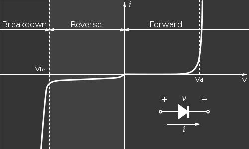
8 Characteristic of a Real Diode Here is a I-V curve for a typical silicon diode. Depending on the application and the required accuracy, a revised version of the diode model may be used. The BD voltage is not to scale (the negative V axis is compressed) 8
9 Some Basics Diodes are made of semiconductor material! Semiconductors are materials whose electrical properties are somewhat in between those of conductors and insulators! Examples: Silicon, Germanium, Gallium Arsenide (GaAs), In semiconductors, a charge carrier can be either a (free) electron or a hole (absence of an electron). Doped semiconductor has impurities intentionally diffused into the material to manipulate the majority of charge carriers to be either electrons (n-type for negative doping, e.g., using Phosphorous in Silicon) or holes (p-type for positive doping, e.g., using Boron in Silicon). 9


10 The pn Junction A diode is formed by a pn junction. At the junction, excess electrons on the n side combine with excess holes on the p side, causing a depletion region that is depleted of charge carriers. This depletion region results in a barrier voltage (~0.7V for Si, and ~0.3V for Ge); if the voltage of the anode (p side) is raised to overcome this barrier, the charge carriers can move again, giving rise to current. 10
11 First Approximation (Constant Voltage Model) A + v D - + _ 0.7V i D C 11
12 Second Approximation 12
13 Second Approximation (Piecewise Linear) + v D - r D + _ 0.7V i D v 0.7 r i D D D 13
14 Third Approximation (Piecewise Linear) i D V BD _ + r BD A r D + _ 0.7V + v D - 14 C
15 Reverse Current When the diode is off, its current (referred to as reverse current) is NOT quite zero i D v BD v D Saturation Current, I o, a few nano or microamps 15

16 Zones of Operation 16

17 Who was Shockley? William Bradford Shockley Jr. (February 13, 1910 August 12, 1989) an American physicist and inventor. Along with John Bardeen and Walter Houser Brattain, Shockley co-invented the transistor, for which all three were awarded the 1956 Nobel Prize in Physics. Shockley's attempts to commercialize a new transistor design in the 1950s and 1960s led to California's Silicon Valley becoming a hotbed of electronics innovation. In his later life, Shockley was a professor at Stanford. (from Wikipedia) 17
18 The actual VI curve i D ~ I e o v V D T n: Ideality or quality factor V kt T qe Thermal Voltage i I e D o v nv D T 1 18
19 The actual VI curve i D I e o v V D T V T kt q e Thermal Voltage k Boltzman constant T temperature, q e electron charge, C o K 19
20 Example T For n=1 and v D >>V T we have: where Given these equations, compute the thermal voltage at room temperature, i.e., 2 o C. If I o =3 na, find the voltage and power of the diode when the current is 2 A. i D I e o v V D V T kt q e 20

21 Practical Limitations Consider the 1N4148 (datasheet: Sample table from data sheet 21
22 Practical Limitations Sample graph from the datasheet (Does this graph make sense?! Is the behaviour similar to what is expected based on Shockley s model?) 22
 Zener diodes are designed to")
23 Zener Diodes Clarence Melvin Zener ( ) was the American physicist who first described the property concerning the breakdown of electrical insulators. His findings were later exploited by Bell Labs in the development of the Zener diode, which was duly named after him (source: Wikipedia) Zener diodes are designed to operate backwards! 23


24 Zener Diodes Diodes I-V plot. Rename the breakdown voltage of the diode as Zener Voltage, V z and use the following polarity and current direction (what would the graph look like? V Z i Z 24
25 Zener Diode Model In the useful Zener region the Zener diode behaves, almost, like an ideal voltage source! It keeps its voltage V Z regardless of the current (up to a maximum power) A r D V zt r Z _ + i Z + _ 0.7V - v Z + C 25
26 Zener Specifications Useful datasheet specifications: Maximum power Zener voltage, V ZT (2V, 5V, 7.2V, ) Current at V ZT, I ZT Minimum Zener current, I ZK ( knee ) Dynamic R k Dynamic R ZT 26
27 To clamp a voltage output Use of the Zener diode V 330 1N5236B 27

28 Diode Applications Diodes are commonly used for rectification! For example to produce DC power from an AC power Half-wave rectification Full-wave rectification V i V o 28
29 Full Wave Rectifier with Smoothing Filter
30 A Full-Wave Bridge Can you think of a way to use a Zener diode in this structure? 30
Electronic Circuits I. Instructor: Dr. Alaa Mahmoud
 Electronic Circuits I Instructor: Dr. Alaa Mahmoud alaa_y_emam@hotmail.com Chapter 27 Diode and diode application Outline: Semiconductor Materials The P-N Junction Diode Biasing P-N Junction Volt-Ampere
KOM2751 Analog Electronics :: Dr. Muharrem Mercimek :: YTU - Control and Automation Dept. 1 1 (CONT D) DIODES
 DIODES") KOM2751 Analog Electronics :: Dr. Muharrem Mercimek :: YTU - Control and Automation Dept. 1 1 (CONT D) DIODES Most of the content is from the textbook: Electronic devices and circuit theory, Robert L.
KOM2751 Analog Electronics :: Dr. Muharrem Mercimek :: YTU - Control and Automation Dept. 1 1 (CONT D) DIODES Most of the content is from the textbook: Electronic devices and circuit theory, Robert L.
Electron Devices and Circuits (EC 8353)
") Electron Devices and Circuits (EC 8353) Prepared by Ms.S.KARKUZHALI, A.P/EEE Diodes The diode is a 2-terminal device. A diode ideally conducts in only one direction. Diode Characteristics Conduction Region
Electron Devices and Circuits (EC 8353) Prepared by Ms.S.KARKUZHALI, A.P/EEE Diodes The diode is a 2-terminal device. A diode ideally conducts in only one direction. Diode Characteristics Conduction Region
Chapter 1: Semiconductor Diodes
 Chapter 1: Semiconductor Diodes Diodes The diode is a 2-terminal device. A diode ideally conducts in only one direction. 2 Diode Characteristics Conduction Region Non-Conduction Region The voltage across
Analog Electronic Circuits
 Analog Electronic Circuits Chapter 1: Semiconductor Diodes Objectives: To become familiar with the working principles of semiconductor diode To become familiar with the design and analysis of diode circuits
Laboratory No. 01: Small & Large Signal Diode Circuits. Electrical Enginnering Departement. By: Dr. Awad Al-Zaben. Instructor: Eng.
 Laboratory No. 01: Small & Large Signal Diode Circuits Electrical Enginnering Departement By: Dr. Awad Al-Zaben Instructor: Eng. Tamer Shahta Electronics Laboratory EE 3191 February 23, 2014 I. OBJECTIVES
Chapter #3: Diodes. from Microelectronic Circuits Text by Sedra and Smith Oxford Publishing
 Chapter #3: Diodes from Microelectronic Circuits Text by Sedra and Smith Oxford Publishing Introduction IN THIS CHAPTER WE WILL LEARN the characteristics of the ideal diode and how to analyze and design
Lesson 5. Electronics: Semiconductors Doping p-n Junction Diode Half Wave and Full Wave Rectification Introduction to Transistors-
 Lesson 5 Electronics: Semiconductors Doping p-n Junction Diode Half Wave and Full Wave Rectification Introduction to Transistors- Types and Connections Semiconductors Semiconductors If there are many free
10/27/2009 Reading: Chapter 10 of Hambley Basic Device Physics Handout (optional)
") EE40 Lec 17 PN Junctions Prof. Nathan Cheung 10/27/2009 Reading: Chapter 10 of Hambley Basic Device Physics Handout (optional) Slide 1 PN Junctions Semiconductor Physics of pn junctions (for reference
EE40 Lec 17 PN Junctions Prof. Nathan Cheung 10/27/2009 Reading: Chapter 10 of Hambley Basic Device Physics Handout (optional) Slide 1 PN Junctions Semiconductor Physics of pn junctions (for reference
Diodes. Analog Electronics Lesson 4. Objectives and Overview:
 Analog Electronics Lesson 4 Diodes Objectives and Overview: This lesson will introduce p- and n-type material, how they form a junction that rectifies current, and familiarize you with basic p-n junction
EXPERIMENTS USING SEMICONDUCTOR DIODES
 EXPERIMENT 9 EXPERIMENTS USING SEMICONDUCTOR DIODES Semiconductor Diodes Structure 91 Introduction Objectives 92 Basics of Semiconductors Revisited 93 A p-n Junction Operation of a p-n Junction A Forward
Lesson 08. Name and affiliation of the author: Professor L B D R P Wijesundera Department of Physics, University of Kelaniya.
 Lesson 08 Title of the Experiment: Identification of active components in electronic circuits and characteristics of a Diode, Zener diode and LED (Activity number of the GCE Advanced Level practical Guide
IENGINEERS- CONSULTANTS QUESTION BANK SERIES ELECTRONICS ENGINEERING 1 YEAR UPTU
 ELECTRONICS ENGINEERING Unit 1 Objectives Q.1 The breakdown mechanism in a lightly doped p-n junction under reverse biased condition is called. (A) avalanche breakdown. (B) zener breakdown. (C) breakdown
semiconductor p-n junction Potential difference across the depletion region is called the built-in potential barrier, or built-in voltage:
 Chapter four The Equilibrium pn Junction The Electric field will create a force that will stop the diffusion of carriers reaches thermal equilibrium condition Potential difference across the depletion
1) A silicon diode measures a low value of resistance with the meter leads in both positions. The trouble, if any, is
 A silicon diode measures a low value of resistance with the meter leads in both positions. The trouble, if any, is") 1) A silicon diode measures a low value of resistance with the meter leads in both positions. The trouble, if any, is A [ ]) the diode is open. B [ ]) the diode is shorted to ground. C [v]) the diode is
1) A silicon diode measures a low value of resistance with the meter leads in both positions. The trouble, if any, is A [ ]) the diode is open. B [ ]) the diode is shorted to ground. C [v]) the diode is
ENG2210 Electronic Circuits. Chapter 3 Diodes
 ENG2210 Electronic Circuits Mokhtar A. Aboelaze York University Chapter 3 Diodes Objectives Learn the characteristics of ideal diode and how to analyze and design circuits containing multiple diodes Learn
PN Junction Diode Table of Contents. What Are Diodes Made Out Of?
 PN Junction iode Table of Contents What are diodes made out of?slide 3 N-type materialslide 4 P-type materialslide 5 The pn junctionslides 6-7 The biased pn junctionslides 8-9 Properties of diodesslides
EC6202- ELECTRONIC DEVICES AND CIRCUITS UNIT TEST-1 EXPECTED QUESTIONS
 EC6202- ELECTRONIC DEVICES AND CIRCUITS UNIT TEST-1 EXPECTED QUESTIONS 1. List the PN diode parameters. 1. Bulk Resistance. 2. Static Resistance/Junction Resistance (or) DC Forward Resistance 3. Dynamic
Diodes and Applications
 Diodes and Applications Diodes and Applications 2 1 Diode Operation 2 2 Voltage-Current (V-I) Characteristics 2 3 Diode Models 2 4 Half-Wave Rectifiers 2 5 Full-Wave Rectifiers 2 6 Power Supply Filters
Intro to Electricity. Introduction to Transistors. Example Circuit Diagrams. Water Analogy
 Introduction to Transistors Transistors form the basic building blocks of all computer hardware. Invented by William Shockley, John Bardeen and Walter Brattain in 1947, replacing previous vaccuumtube technology
Intrinsic Semiconductor
 Semiconductors Crystalline solid materials whose resistivities are values between those of conductors and insulators. Good electrical characteristics and feasible fabrication technology are some reasons
Mechatronics Chapter 3-1 Semiconductor devices Diode
 MEMS1082 Mechatronics Chapter 3-1 Semiconductor devices Diode Semiconductor: Si Semiconductor N-type and P-type Semiconductors There are two types of impurities: N-type - In N-type doping, phosphorus or
THERMIONIC AND GASEOUS STATE DIODES
 THERMIONIC AND GASEOUS STATE DIODES Thermionic and gaseous state (vacuum tube) diodes Thermionic diodes are thermionic-valve devices (also known as vacuum tubes, tubes, or valves), which are arrangements
Diode Characteristics and Applications
 Diode Characteristics and Applications Topics covered in this presentation: Diode Characteristics Diode Clamp Protecting Against Back-EMF Half-Wave Rectifier The Zener Diode 1 of 18 Diode Characteristics
Student Lecture by: Giangiacomo Groppi Joel Cassell Pierre Berthelot September 28 th 2004
 Student Lecture by: Giangiacomo Groppi Joel Cassell Pierre Berthelot September 28 th 2004 Lecture outline Historical introduction Semiconductor devices overview Bipolar Junction Transistor (BJT) Field
Electro - Principles I
 The PN Junction Diode Introduction to the PN Junction Diode Note: In this chapter we consider conventional current flow. Page 11-1 The schematic symbol for the pn junction diode the shown in Figure 1.
Diode conducts when V anode > V cathode. Positive current flow. Diodes (and transistors) are non-linear device: V IR!
 are non-linear device: V IR!") Diodes: What do we use diodes for? Lecture 5: Diodes and Transistors protect circuits by limiting the voltage (clipping and clamping) turn AC into DC (voltage rectifier) voltage multipliers (e.g. double
Diodes: What do we use diodes for? Lecture 5: Diodes and Transistors protect circuits by limiting the voltage (clipping and clamping) turn AC into DC (voltage rectifier) voltage multipliers (e.g. double
Ch5 Diodes and Diodes Circuits
 Circuits and Analog Electronics Ch5 Diodes and Diodes Circuits 5.1 The Physical Principles of Semiconductor 5.2 Diodes 5.3 Diode Circuits 5.4 Zener Diode References: Floyd-Ch2; Gao-Ch6; 5.1 The Physical
Electronics The basics of semiconductor physics
 Electronics The basics of semiconductor physics Prof. Márta Rencz, Gábor Takács BME DED 17/09/2015 1 / 37 The basic properties of semiconductors Range of conductivity [Source: http://www.britannica.com]
EE/COE 152: Basic Electronics. Lecture 3. A.S Agbemenu. https://sites.google.com/site/agbemenu/courses/ee-coe-152
 EE/COE 152: Basic Electronics Lecture 3 A.S Agbemenu https://sites.google.com/site/agbemenu/courses/ee-coe-152 Books: Microelcetronic Circuit Design (Jaeger/Blalock) Microelectronic Circuits (Sedra/Smith)
Physics 160 Lecture 5. R. Johnson April 13, 2015
 Physics 160 Lecture 5 R. Johnson April 13, 2015 Half Wave Diode Rectifiers Full Wave April 13, 2015 Physics 160 2 Note that there is no ground connection on this side of the rectifier! Output Smoothing
Electrical and Electronic Laboratory Faculty of Engineering Chulalongkorn University. Semiconductor Diode (SD)
") 2141274 Electrical and Electronic Laboratory Faculty of Engineering Chulalongkorn University Semiconductor Diode (SD) Contents A. Introduction 1. History 2. Thermionic or gaseous state diodes 3. Semiconductor
2141274 Electrical and Electronic Laboratory Faculty of Engineering Chulalongkorn University Semiconductor Diode (SD) Contents A. Introduction 1. History 2. Thermionic or gaseous state diodes 3. Semiconductor
Chapter 2. Diodes & Applications
 Chapter 2 Diodes & Applications The Diode A diode is made from a small piece of semiconductor material, usually silicon, in which half is doped as a p region and half is doped as an n region with a pn
2 MARKS EE2203 ELECTRONIC DEVICES AND CIRCUITS UNIT 1
 2 MARKS EE2203 ELECTRONIC DEVICES AND CIRCUITS UNIT 1 1. Define PN junction. When a p type semiconductor is joined to a N type semiconductor the contact surface is called PN junction. 2. What is an ideal
Lecture -1: p-n Junction Diode
 Lecture -1: p-n Junction Diode Diode: A pure silicon crystal or germanium crystal is known as an intrinsic semiconductor. There are not enough free electrons and holes in an intrinsic semi-conductor to
Semiconductor Devices Lecture 5, pn-junction Diode
 Semiconductor Devices Lecture 5, pn-junction Diode Content Contact potential Space charge region, Electric Field, depletion depth Current-Voltage characteristic Depletion layer capacitance Diffusion capacitance
Microelectronic Circuits, Kyung Hee Univ. Spring, Chapter 3. Diodes
 Chapter 3. Diodes 1 Introduction IN THIS CHAPTER WE WILL LEARN the characteristics of the ideal diode and how to analyze and design circuits containing multiple ideal diodes together with resistors and
Università degli Studi di Roma Tor Vergata Dipartimento di Ingegneria Elettronica. Analogue Electronics. Paolo Colantonio A.A.
 Università degli Studi di Roma Tor Vergata Dipartimento di Ingegneria Elettronica Analogue Electronics Paolo Colantonio A.A. 2015-16 Introduction: materials Conductors e.g. copper or aluminum have a cloud
EDC UNIT IV- Transistor and FET Characteristics EDC Lesson 9- ", Raj Kamal, 1
 EDC UNIT IV- Transistor and FET Characteristics Lesson-9: JFET and Construction of JFET 2008 EDC Lesson 9- ", Raj Kamal, 1 1. Transistor 2008 EDC Lesson 9- ", Raj Kamal, 2 Transistor Definition The transferred-resistance
Diode Limiters or Clipper Circuits
 Diode Limiters or Clipper Circuits Circuits which are used to clip off portions of signal voltages above or below certain levels are called limiters or clippers. Types of Clippers Positive Clipper Negative
EDC Lecture Notes UNIT-1
 P-N Junction Diode EDC Lecture Notes Diode: A pure silicon crystal or germanium crystal is known as an intrinsic semiconductor. There are not enough free electrons and holes in an intrinsic semi-conductor
Diode Bridges. Book page
 Diode Bridges Book page 450-454 Rectification The process of converting an ac supply into dc is called rectification The device that carries this out is called a rectifier Half wave rectifier only half
UNIT IX ELECTRONIC DEVICES
 UNT X ELECTRONC DECES Weightage Marks : 07 Semiconductors Semiconductors diode-- characteristics in forward and reverse bias, diode as rectifier. - characteristics of LED, Photodiodes, solarcell and Zener
Made of semiconducting materials: silicon, gallium arsenide, indium phosphide, gallium nitride, etc. (EE 332 stuff.)
") Diodes Simple two-terminal electronic devices. Made of semiconducting materials: silicon, gallium arsenide, indium phosphide, gallium nitride, etc. (EE 332 stuff.) Semiconductors are interesting because
Diodes Simple two-terminal electronic devices. Made of semiconducting materials: silicon, gallium arsenide, indium phosphide, gallium nitride, etc. (EE 332 stuff.) Semiconductors are interesting because
Lecture 3: Diodes. Amplitude Modulation. Diode Detection.
 Whites, EE 322 Lecture 3 Page 1 of 10 Lecture 3: Diodes. Amplitude Modulation. Diode Detection. Diodes are the fourth basic discrete component listed in Lecture 2. These and transistors are both nonlinear
Review Energy Bands Carrier Density & Mobility Carrier Transport Generation and Recombination
 Review Energy Bands Carrier Density & Mobility Carrier Transport Generation and Recombination Current Transport: Diffusion, Thermionic Emission & Tunneling For Diffusion current, the depletion layer is
Module 04.(B1) Electronic Fundamentals
 Electronic Fundamentals") 1.1a. Semiconductors - Diodes. Module 04.(B1) Electronic Fundamentals Question Number. 1. What gives the colour of an LED?. Option A. The active element. Option B. The plastic it is encased in. Option
1.1a. Semiconductors - Diodes. Module 04.(B1) Electronic Fundamentals Question Number. 1. What gives the colour of an LED?. Option A. The active element. Option B. The plastic it is encased in. Option
Electronic devices-i. Difference between conductors, insulators and semiconductors
 Electronic devices-i Semiconductor Devices is one of the important and easy units in class XII CBSE Physics syllabus. It is easy to understand and learn. Generally the questions asked are simple. The unit
1 Diodes. 1.1 Diode Models Ideal Diode. ELEN 236 Diodes
 ELEN 236 Diodes 1 Diodes 1.1 Diode Models 1.1.1 Ideal Diode Current through diode is zero for any voltage less than zero i.e. reverse biased case Current through diode is not limited by diode if voltage
LAB IV. SILICON DIODE CHARACTERISTICS
 LAB IV. SILICON DIODE CHARACTERISTICS 1. OBJECTIVE In this lab you will measure the I-V characteristics of the rectifier and Zener diodes, in both forward and reverse-bias mode, as well as learn what mechanisms
Lec (03) Diodes and Applications
 Diodes and Applications") Lec (03) Diodes and Applications Diode Models 1 Diodes and Applications Diode Operation V-I Characteristics of a Diode Diode Models Half-Wave and Full-Wave Rectifiers Power Supply Filters and Regulators
Lec (03) Diodes and Applications Diode Models 1 Diodes and Applications Diode Operation V-I Characteristics of a Diode Diode Models Half-Wave and Full-Wave Rectifiers Power Supply Filters and Regulators
Discuss the difference between conductors,insulators and semi conductors. Understand the P-N junction and explain the origin of the depletion region
 UNIT III SEMICONDUCTOR DIODES Review of intrinsic & externsic semiconductors Theory of PN junction diode Energy band structure current equation space charge and diffusion capacitances effect of temperature
CHAPTER 1 DIODE CIRCUITS. Semiconductor act differently to DC and AC currents
 CHAPTER 1 DIODE CIRCUITS Resistance levels Semiconductor act differently to DC and AC currents There are three types of resistances 1. DC or static resistance The application of DC voltage to a circuit
Light Emitting Diodes
 Light Emitting Diodes Topics covered in this presentation: LED operation LED Characteristics Display devices Protection and limiting 1 of 9 Light Emitting Diode - LED A special type of diode is the Light
Ideal Diode Summary. p-n Junction. Consequently, characteristics curve of the ideal diode is given by. Ideal diode state = OF F, if V D < 0
 Course Contents ELE230 Electronics I http://www.ee.hacettepe.edu.tr/ usezen/ele230/ Dr. Umut Sezen & Dr. Dinçer Gökcen Department of Electrical and Electronic Engineering Hacettepe University and Diode
EC T34 ELECTRONIC DEVICES AND CIRCUITS
 RAJIV GANDHI COLLEGE OF ENGINEERING AND TECHNOLOGY PONDY-CUDDALORE MAIN ROAD, KIRUMAMPAKKAM-PUDUCHERRY DEPARTMENT OF ECE EC T34 ELECTRONIC DEVICES AND CIRCUITS II YEAR Mr.L.ARUNJEEVA., AP/ECE 1 PN JUNCTION
EE70 - Intro. Electronics
 EE70 - Intro. Electronics Course website: ~/classes/ee70/fall05 Today s class agenda (November 28, 2005) review Serial/parallel resonant circuits Diode Field Effect Transistor (FET) f 0 = Qs = Qs = 1 2π
Basic Electronics Prof. Dr. Chitralekha Mahanta Department of Electronics and Communication Engineering Indian Institute of Technology, Guwahati
 Basic Electronics Prof. Dr. Chitralekha Mahanta Department of Electronics and Communication Engineering Indian Institute of Technology, Guwahati Module: 2 Bipolar Junction Transistors Lecture-1 Transistor
Semiconductor Diodes
 Semiconductor Diodes A) Motivation and Game Plan B) Semiconductor Doping and Conduction C) Diode Structure and I vs. V D) Diode Circuits Reading: Schwarz and Oldham, Chapter 13.1-13.2 Motivation Digital
15 - SEMICONDUCTOR ELECTRONICS: MATERIALS, DEVICES AND SIMPLE CIRCUITS Page 1
 15.1 Introduction MATERIALS, DEVICES AND SIMPLE CIRCUITS Page 1 The word electronics is coined from the words electron mechanics. The subject of electronics deals with the study of devices in which specific
Chapter Semiconductor Electronics
 Chapter Semiconductor Electronics Q1. p-n junction is said to be forward biased, when [1988] (a) the positive pole of the battery is joined to the p- semiconductor and negative pole to the n- semiconductor
Discuss the basic structure of atoms Discuss properties of insulators, conductors, and semiconductors
 Discuss the basic structure of atoms Discuss properties of insulators, conductors, and semiconductors Discuss covalent bonding Describe the properties of both p and n type materials Discuss both forward
Table of Contents. iii
 Table of Contents Subject Page Experiment 1: Diode Characteristics... 1 Experiment 2: Rectifier Circuits... 7 Experiment 3: Clipping and Clamping Circuits 17 Experiment 4: The Zener Diode 25 Experiment
Diodes. Introduction. Silicon p-n junction diodes. Structure
 Diodes ntroduction A diode is a two terminal circuit element that allows current flow in one direction only. Diodes are thus non-linear circuit elements because the current through them is not proportional
Objective Type Questions 1. Why pure semiconductors are insulators at 0 o K? 2. What is effect of temperature on barrier voltage? 3.
 Objective Type Questions 1. Why pure semiconductors are insulators at 0 o K? 2. What is effect of temperature on barrier voltage? 3. What is difference between electron and hole? 4. Why electrons have
SEMICONDUCTOR ELECTRONICS: MATERIALS, DEVICES AND SIMPLE CIRCUITS. Class XII : PHYSICS WORKSHEET
 SEMICONDUCT ELECTRONICS: MATERIALS, DEVICES AND SIMPLE CIRCUITS Class XII : PHYSICS WKSHEET 1. How is a n-p-n transistor represented symbolically? (1) 2. How does conductivity of a semiconductor change
Introduction to Solid State Electronics
 Introduction to Solid State Electronics Semiconductors: These are the materials, which do not have free electrons to support the flow of electrical current through them at room temperature. However, valence
The Discussion of this exercise covers the following points:
 Exercise 1 The Diode EXERCISE OBJECTIVE When you have completed this exercise, you will be familiar with the operation of a diode. DISCUSSION OUTLINE The Discussion of this exercise covers the following
Lecture 2 p-n junction Diode characteristics. By Asst. Prof Dr. Jassim K. Hmood
 Electronic I Lecture 2 p-n junction Diode characteristics By Asst. Prof Dr. Jassim K. Hmood THE p-n JUNCTION DIODE The pn junction diode is formed by fabrication of a p-type semiconductor region in intimate
Reg. No. : Question Paper Code : B.E./B.Tech. DEGREE EXAMINATION, NOVEMBER/DECEMBER Second Semester
 WK 5 Reg. No. : Question Paper Code : 27184 B.E./B.Tech. DEGREE EXAMINATION, NOVEMBER/DECEMBER 2015. Time : Three hours Second Semester Electronics and Communication Engineering EC 6201 ELECTRONIC DEVICES
CHAPTER 8 The PN Junction Diode
 CHAPTER 8 The PN Junction Diode Consider the process by which the potential barrier of a PN junction is lowered when a forward bias voltage is applied, so holes and electrons can flow across the junction
FIELD EFFECT TRANSISTORS MADE BY : GROUP (13)/PM
/PM") FIELD EFFECT TRANSISTORS MADE BY : GROUP (13)/PM THE FIELD EFFECT TRANSISTOR (FET) In 1945, Shockley had an idea for making a solid state device out of semiconductors. He reasoned that a strong electrical
FIELD EFFECT TRANSISTORS MADE BY : GROUP (13)/PM THE FIELD EFFECT TRANSISTOR (FET) In 1945, Shockley had an idea for making a solid state device out of semiconductors. He reasoned that a strong electrical
13. SEMICONDUCTOR DEVICES
 Synopsis: 13. SEMICONDUCTOR DEVICES 1. Solids are classified into two categories. a) Crystalline solids b) Amorphous solids 2. Crystalline solids : Crystalline solids have orderly arrangement of atoms
Downloaded from
 SOLID AND SEMICONDUCTOR DEVICES (EASY AND SCORING TOPIC) 1. Distinction of metals, semiconductor and insulator on the basis of Energy band of Solids. 2. Types of Semiconductor. 3. PN Junction formation
55:041 Electronic Circuits
 55:041 Electronic Circuits Chapter 1 & 2 A. Kruger Diode Review, Page-1 Semiconductors licon () atoms have 4 electrons in valence band and form strong covalent bonds with surrounding atoms. Section 1.1.2
Chapter 1: Diode circuits
 Analog Electronics Circuits Nagamani A N Lecturer, PESIT, Bangalore 85 Email nagamani@pes.edu Chapter 1: Diode circuits Objective To understand the diode operation and its equivalent circuits To understand
PHYS 3050 Electronics I
 PHYS 3050 Electronics I Chapter 4. Semiconductor Diodes and Transistors Earth, Moon, Mars, and Beyond Dr. Jinjun Shan, Associate Professor of Space Engineering Department of Earth and Space Science and
Figure 2.1: Energy Band gap Block Diagram
 Figure 2.1: Energy Band gap Block Diagram Figure 2.2: Log Is Vs 10 3 /T Figure 2.3: Schematic Representation of a p-n Junction Diode Department of Physical Sciences, Bannari Amman Institute of Technology,
Physics 281 EXPERIMENT 7 I-V Curves of Non linear Device
 Physics 281 EXPERIMENT 7 I-V Curves of Non linear Device Print this page to start your lab report (1 copy) Bring a diskette to save your data. OBJECT: To study the method of obtaining the characteristics
Lecture # 23 Diodes and Diode Circuits. A) Basic Semiconductor Materials B) Diode Current and Equation C) Diode Circuits
 Basic Semiconductor Materials B) Diode Current and Equation C) Diode Circuits") EECS 42 ntro. Digital Electronics, Fall 2003 EECS 42 ntroduction to Digital Electronics Lecture # 23 Diodes and Diode Circuits A) Basic Semiconductor Materials B) Diode Current and Equation C) Diode Circuits
EECS 42 ntro. Digital Electronics, Fall 2003 EECS 42 ntroduction to Digital Electronics Lecture # 23 Diodes and Diode Circuits A) Basic Semiconductor Materials B) Diode Current and Equation C) Diode Circuits
BASIC ELECTRONICS ENGINEERING
 BASIC ELECTRONICS ENGINEERING Objective Questions UNIT 1: DIODES AND CIRCUITS 1 2 3 4 5 6 7 8 9 10 11 12 The process by which impurities are added to a pure semiconductor is A. Diffusing B. Drift C. Doping
Class XII - Physics Semiconductor Electronics. Chapter-wise Problems
 lass X - Physics Semiconductor Electronics Materials, Device and Simple ircuit hapter-wise Problems Multiple hoice Question :- 14.1 The conductivity of a semiconductor increases with increase in temperature
EEE118: Electronic Devices and Circuits
 EEE118: Electronic Devices and Circuits Lecture IIII James E Green Department of Electronic Engineering University of Sheffield j.e.green@sheffield.ac.uk Last Lecture: Review 1 Defined some terminology
Basic Electronics Important questions
 Basic Electronics Important questions B.E-2/4 Mech- B Faculty: P.Lakshmi Prasanna Note: Read the questions in the following order i. Assignment questions ii. Class test iii. Expected questions iv. Tutorials
 Energy band diagrams Metals: 9. ELECTRONIC DEVICES GIST ρ= 10-2 to 10-8 Ω m Insulators: ρ> 10 8 Ω m Semiconductors ρ= 1 to 10 5 Ω m 109 A. Intrinsic semiconductors At T=0k it acts as insulator At room
3.2 Terminal Characteristics of Junction Diodes (pp )
") 8/7/004 3_ Terminal Characteristics of Junction iodes blank.doc /6 3. Terminal Characteristics of Junction iodes (pp.47-53) + v i HO: The Junction iode Curve HO: The Junction iode Equation A. The Forward
8/7/004 3_ Terminal Characteristics of Junction iodes blank.doc /6 3. Terminal Characteristics of Junction iodes (pp.47-53) + v i HO: The Junction iode Curve HO: The Junction iode Equation A. The Forward
Sharjah Indian School, Sharjah ELECTRONIC DEVICES - Class XII (Boys Wing) Page 01
 Page 01") ELECTRONIC DEVICES - Class XII (Boys Wing) Page 01 Electronics is the fast developing branch of Physics. Before the discovery of transistors in 1948, vacuum tubes (thermionic valves) were used as the building
ELECTRONIC DEVICES - Class XII (Boys Wing) Page 01 Electronics is the fast developing branch of Physics. Before the discovery of transistors in 1948, vacuum tubes (thermionic valves) were used as the building
جامعة اإلسكندرية كلية الهندسة قسم الهندسة الكهربية أبريل ٢٠١٥
 Alexandria University Faculty of Engineering Electrical Engineering Department April 2015 1a EE 132 Electronic Devices and Circuits First Year Time allowed: 1½ hours جامعة اإلسكندرية كلية الهندسة قسم الهندسة
VALLIAMMAI ENGINEERING COLLEGE SRM Nagar, Kattankulathur
 VALLIAMMAI ENGINEERING COLLEGE SRM Nagar, Kattankulathur 603 203. DEPARTMENT OF ELECTRONICS & COMMUNICATION ENGINEERING SUBJECT QUESTION BANK : EC6201 ELECTRONIC DEVICES SEM / YEAR: II / I year B.E.ECE
Diodes (non-linear devices)
") C H A P T E R 4 Diodes (non-linear devices) Ideal Diode Figure 4.2 The two modes of operation of ideal diodes and the use of an external circuit to limit (a) the forward current and (b) the reverse voltage.
C H A P T E R 4 Diodes (non-linear devices) Ideal Diode Figure 4.2 The two modes of operation of ideal diodes and the use of an external circuit to limit (a) the forward current and (b) the reverse voltage.
Chapter 14 Semiconductor Electronics Materials Devices And Simple Circuits
 Class XII Chapter 14 Semiconductor Electronics Materials Devices And Simple Circuits Physics Question 14.1: In an n-type silicon, which of the following statement is true: (a) Electrons are majority carriers
FET Channel. - simplified representation of three terminal device called a field effect transistor (FET)
") FET Channel - simplified representation of three terminal device called a field effect transistor (FET) - overall horizontal shape - current levels off as voltage increases - two regions of operation 1.
FET Channel - simplified representation of three terminal device called a field effect transistor (FET) - overall horizontal shape - current levels off as voltage increases - two regions of operation 1.
Analog Electronics. Lecture 3. Muhammad Amir Yousaf
 Analog Electronics Lecture 3 Discrete Semiconductor Devices Rectifier (Diodes) Light Emitting Diodes Zener Diodes Photo Diodes Transistors Bipolar Junction Transistors (BJTs) MOSFETs Diodes A diode is
Term Roadmap : Materials Types 1. INSULATORS
 Term Roadmap : Introduction to Signal Processing Differentiating and Integrating Circuits (OpAmps) Clipping and Clamping Circuits(Diodes) Design of analog filters Sinusoidal Oscillators Multivibrators
NAME: Last First Signature
 UNIVERSITY OF CALIFORNIA, BERKELEY College of Engineering Department of Electrical Engineering and Computer Sciences EE 130: IC Devices Spring 2003 FINAL EXAMINATION NAME: Last First Signature STUDENT
Zaid abdul zahra hassan. Dept.of physics-collage of education for pure sciences. Babylon university
 Tunnel diode: Zaid abdul zahra hassan Dept.of physics-collage of education for pure sciences Babylon university 1N3716 tunnel diode (with jumper for scale) A tunnel diode or Esaki diode is a type of semiconductor
PETER PAZMANY CATHOLIC UNIVERSITY Consortium members SEMMELWEIS UNIVERSITY, DIALOG CAMPUS PUBLISHER
 PETER PAZMANY CATHOLIC UNIVERSITY SEMMELWEIS UNIVERSITY Development of Complex Curricula for Molecular Bionics and Infobionics Programs within a consortial* framework** Consortium leader PETER PAZMANY
Federal Urdu University of Arts, Science & Technology Islamabad Pakistan SECOND SEMESTER ELECTRONICS - I
 SECOND SEMESTER ELECTRONICS - I BASIC ELECTRICAL & ELECTRONICS LAB DEPARTMENT OF ELECTRICAL ENGINEERING Prepared By: Checked By: Approved By: Engr. Yousaf Hameed Engr. M.Nasim Khan Dr.Noman Jafri Lecturer
Lesson Plan. Week Theory Practical Lecture Day. Topic (including assignment / test) Day. Thevenin s theorem, Norton s theorem
 Day. Thevenin s theorem, Norton s theorem") Name of the faculty: GYANENDRA KUMAR YADAV Discipline: APPLIED SCIENCE(C.S.E,E.E.ECE) Year : 1st Subject: FEEE Lesson Plan Lesson Plan Duration: 31 weeks (from July, 2018 to April, 2019) Week Theory Practical
Name of the faculty: GYANENDRA KUMAR YADAV Discipline: APPLIED SCIENCE(C.S.E,E.E.ECE) Year : 1st Subject: FEEE Lesson Plan Lesson Plan Duration: 31 weeks (from July, 2018 to April, 2019) Week Theory Practical
Digital Integrated Circuits A Design Perspective. The Devices. Digital Integrated Circuits 2nd Devices
 Digital Integrated Circuits A Design Perspective The Devices The Diode The diodes are rarely explicitly used in modern integrated circuits However, a MOS transistor contains at least two reverse biased