PCB Artist Quickstart Guide Revision 01
|
|
|
- Betty Nicholson
- 6 years ago
- Views:
Transcription
1 UT DALLAS Erik Jonsson School of Engineering & Computer Science PCB Artist Quickstart Guide Revision 01 Pete Semig Ph.D. Student-Dr. Jafari Analog Application Engineer-TI 1
2 Important Terminology PCB Artist is a free PCB schematic & layout tool provided by Advanced Circuits It can be downloaded from or Pros: Free Intuitive and simple to use/install Autorouter Large libraries East to create new parts (schematic symbols & footprints) No minimum quantity for students (see website) Cons: No interactive DRC Boards are ~$33/ea (2-layer, 5 day turn) or $66/ea (4-layer, 5 day turn) You do not get the gerber files (i.e. you must fabricate designs with Advanced Circuits) 2

3 Important Terminology mil Layer A mil is 1/1000 th of an inch. 1mil=.001 PCBs are made of layers Here are the common layers Metal The actual wires/conductors Silkscreen The white writing on the PCB Soldermask The green stuff [2] [2]

4 Important Terminology Trace The width of a metal wire Space The minimum distance between traces Trace/Space 6 mil trace/space means the traces must be at least 6 mils wide and there must be at least 6 mils of space between traces [1]


5 Important Terminology Pad Surface mount (SM) and/or with hole [1] [1] [2] [2]

6 Important Terminology Via A via is a metal-plated hole drilled in the PCB that connects metal layers Four common types are stub, through-hole, blind, and buried Figures are from [3] Through

7 Advanced Circuits (AC) Specials These selections will depend on your design needs. If interested in the $33 or $66 specials, be sure to adjust settings appropriately
8 AC Capabilities

9 AC Tolerances
10 UT DALLAS Erik Jonsson School of Engineering & Computer Science PCB Artist


11 New Project File->New Select New Project and specify path for *.prj file


12 Add Schematic File->New Select New Schematic, assign file name and check Add to Open Project


13 Add PCB Layout File->New Select New PCB Design, assign file name and check Add to Open Project Selecting OK will launch the PCB Wizard


14 PCB Wizard Set units to mils and precision to 0 Precision is the number of places to the right of the decimal A value of 1 allows for measurements such as 15.8mils, but not 15.75mils. For 15.75mils, precision should be set to 2 Use basic-minimums for board template


15 PCB Wizard Select appropriate board service (most will probably be 2 or 4 layer standard)


16 PCB Wizard For a 2-layer board the parameters will be straightforward

17 PCB Wizard For a 4-layer board you can specify powerplane layers


18 PCB Wizard


19 PCB Wizard Select whether or not you want electrical testing (probably not)


20 PCB Wizard Specify board part number, revision, and quantity Adjust turnaround time as needed 3 days is recommended Select Next, then Finish.
21 PCB Settings Grid Units Styles Spacings Nets Net Classes


22 PCB Settings-Grid Settings->Grids
23 PCB Settings-Units Settings->Units


24 PCB Settings-Styles Settings->Styles


25 PCB Settings-Spacings Settings->Spacings

26 PCB Settings-Rules

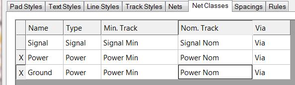
27 PCB Settings-Nets & Net Classes
28 Example Design Let s create the schematic and PCB for the following filter Active low-pass Fc=1kHz 4 th order 2-stage Sallen-Key We can use TI s FilterPro to obtain a generic schematic Then use TI s TINA-TI to verify in simulation
29 FilterPro Design
30 Amplifier Selection Let s implement this filter with the OPA141 Single-supply, 10MHz, RRO, Low-noise, JFET input (Ib=20pA max) Supply: 4.5V to 36V Packages Single (SO-8, MSOP-8) Dual (SO-8, MSOP-8) Quad (TSSOP-14, SO-14) Vicm includes GND
31 TINA-TI Simulation V+ C n C3 68.3n V1 5 V2 5 V- Vin + R1 14.7k R2 14.7k C1 10n V V- U1 OPA141 R3 6.09k R4 6.09k C4 10n V V- Vout U2 OPA141 T 0-40 Gain (db) k 10k 100k 1M Frequency (Hz)

 Select New Lib Give new")
32 New Schematic Symbol Library Let s create a new Library for custom schematic symbols Open Library Manager (Ctrl-L) Select New Lib Give new library a name

33 New Schematic Symbol
34 New Schematic Symbol For this device we will use the dual version (our filter has 2 amplifiers) From a schematic perspective, we will need 2 sub-symbols One will look like an ideal op-amp The second one will have power and ground Here is the idea using symbols from TINA - + IOP OP1!OPAMP 6 Note: Please don t use the package pinout as the schematic symbol! This makes it difficult to read the schematic.
35 New Schematic Symbol Create 2 separate symbols in the library Use Add Pad for the pins Use Single Line and Triangle for the symbol Move the symbol origin (S) to one of the pins The numbers correspond to the pins, NX is the pin name Save the symbols as myopamp3 and myopamp5

36 New Schematic Symbol


37 New PCB Symbol Library Let s create a new Library for custom PCB symbols Open Library Manager (Ctrl-L) Select PCB Symbol tab Give new library a name
38 OPA2141 Packages We need to determine which package we will use The datasheet typically has all the information required We see the OPA2141 comes in two packages MSOP-8 SO-8 TI refers to these packages as DGK and D

39 OPA2141 Landing Patterns Let s compare the D and DGK packages D is found in the PDS, but DGK is not! Here is a link to a useful app note


40 New PCB Symbol Let s use the DGK (MSOP-8) for it is smaller Create a new Library for custom PCB symbols Open Library Manager (Ctrl-L) Select PCB Symbol tab Give new library a name Let s use the Wizard Use mils, precision 1


41 New PCB Symbol

42 New PCB Symbol PCB Artist->App Note *Set H=T=0 e=e=25.6 E=Z=230 L=Y=66 b=x=18


43 New PCB Symbol


44 New Component Now we have the schematic and PCB symbols, we can combine them to create a component Create a new component library (make sure component tab is selected) Click New Item Only select one of the schematic symbols, we will add the other one later


45 New Component Click Add Gate icon Add 5-pin schematic symbol a will zoom to all in schematic and PCB windows You may have to rightclick in top window to see spreadsheet


46 New Component Fill out spreadsheet according to datasheet block diagram & save component


47 Create Schematic Create Schematic in project Use Add Component to instantiate OPA2141 Note you can place each symbol separately Add Component->Find is very useful R s are in library resistor C s are in library capacitor

48 Create Schematic Common passive sizes are 0402, 0603, 0805, and 1206 Probably want size 0805 at least for hand soldering Note: 0.1mm~=4mils


49 Create Schematic Use schema library for border (e.g. Letter) and power/ground Use resistor and capacitor libraries for R s and C s
50 Create Schematic Use connector library to add connectors or make your own V+ C n C3 68.3n V1 5 V2 5 V- Vin + R1 14.7k R2 14.7k C1 10n V V- U1 OPA141 R3 6.09k R4 6.09k C4 10n V V- Vout U2 OPA141

51 Create Schematic Are we missing anything? Check datasheets for layout recommendations From the OPA141 PDS: So we need to add decoupling capacitors near the device s supply
52 Create Schematic These are bad! Must use wire to connect!
53 Create Schematic


54 Create Schematic Finally, we need to ensure that our power and ground nets are set appropriately Right-click a ground symbol Select Change Net Make sure net name and net class are set appropriately Also do this for +5V and -5V


55 Create PCB Save and close schematic Open Layout Import footprints from Schematic Tools->[Schematic<->PCB]->Consistency Check I recommend performing Consistency Checks frequently during a design Yes OK a to zoom all Select all footprints and move them outside PCB border a to zoom all


56 Create PCB Yellow lines are connections that need to be made Sometimes called rubber bands Place components inside green PCB border PCB Artist has an autoplace components feature, but it doesn t seem to work well Place the OPA2141, power connector, input connector, output connector, and decoupling caps In general, place inputs on left side of board, outputs on right, and power at top or bottom


57 Create PCB Notice lack of bands for supplies? This is because they weren t connected in schematic! (Remember the X s?)


58 Create PCB Supply nets and grounds are now connected. Also fit board outline. *Run DRC often!* Tools->DRC (check Spacing and Manufacturing)


59 Create PCB Since we have 2 layers, let s make the bottom layer GND Need to perform a pour Add->Copper Pour->Rectangle Press L to change layer to bottom Create rectangle inside board outline


60 Create PCB Right click copper pour outline and select Pour Copper Assign to GND net and click OK To hide bottom layer, press F9, select Layers tab, and uncheck Bottom Copper Now we can use vias to connect to GND

61 Create PCB We know C3, C4, and C5 are all grounded We can place a via to connect them to the ground plane Add->Via Esc stops placement Once placed, right-click via and add to GND net (Net->Change Net)
 You can left-click band and press delete If bands are missing, try performing a consistency check from tools")
62 Create PCB To route a trace to the via, double-click the pad of the footprint (notice the trace is 25mils wide) Drag trace to via and double-click again Do this for all GND nets Bands didn t disappear, press ctrl-d to optimize nets (in tools menu) You can left-click band and press delete If bands are missing, try performing a consistency check from tools menu

63 Create PCB You may get a join nets box The order depends on where you start and end your trace To switch the order, route in the reverse order


64 Create PCB I would hand-route power and GND first. Since power traces are wider than MSOP-8 pads, route as close to pad as possible with thick trace. Then route from pad to thick trace. While routing from pad to thick trace, press S and change width to 18 Run DRC often! Don t forget Ctrl-D and Consistency Checks!
 Tools->Autoroute Nets->Browse Nets (we will do this since we already routed power and GND) This didn t work well for me, and I prefer to do it by hand")
65 Create PCB You can try autorouting (3 methods) Right click a band and select autoroute to route 1 trace at a time Tools->Autoroute Nets->All Nets to route all nets (it will remove your existing routes) Tools->Autoroute Nets->Browse Nets (we will do this since we already routed power and GND) This didn t work well for me, and I prefer to do it by hand anyways


66 Create PCB Almost done Are we stuck??


67 Create PCB Nope!
68 Create PCB-Reflection Some of the traces were long We could have looked at using a 4-layer board We also didn t have to devote an entire routing plane to ground We could also have separated V+, V-, and GND connectors and moved them to more convenient locations.
69 Fabricate PCB Be sure to run a DRC with all boxes checked Output->Submit Order Follow the directions You will need to setup an AC account Alternately, I could submit the order for you.
70 UT DALLAS Erik Jonsson School of Engineering & Computer Science PCB Layout Tips from TI
71 All Materials have a Finite Resistance Y For 1 oz. Copper: For PCB Trace X Z ρ = x cm for Y = cm R = ρz/xy R = 0.45 Z/X m = number of squares R = sheet resistance for 1 square ( Z = X ) = 0.45m /square For Wire L d R = L d 2 L in meters d in mm
72 PCB Trace Resistance 1 inch 1.3µV 10µA 1 inch (7 mil) trace of 1/2 oz copper with 10µA of current => voltage drop of 1.3µV 4 LSBs (298nV) at 24 bits!
73 PCB Inductance W L PCB: ( 2L ) ( W+H ) W+H L Inductance = L ln H Example: L = 10cm H W = 0.25mm H = 0.038mm This PC track has 141nH of inductance Wire: L 2R ( ) 2L Inductance = L ln H R Example: L = 10cm 2R = 0.5mm This wire has 105nH of inductance
74 PCB Capacitance Two Cu plates with PCB material dielectric Two 10 mil traces on a multi layer PCB, 10 mil between layers A = 0.25 mm x 0.25 mm Permittivity of FR4 4.7 o = 8.84 x Note: 10 mil = 0.25 mm.
 via with 1.")
 pad on FR-4 has 0.")
75 PCB Vias Component: Vias Purpose: Interconnect traces on different layers Problem: Inductance and Capacitance 0.4mm ( ) via with 1.6mm (0.063 ) thick PCB has 1.2nH 1.6mm (0.063 ) Clearance hole around 0.8mm (0.031 ) pad on FR-4 has 0.4pF e r = PCB material permeability (FR-4 4.5) 4
76 Bypass Capacitors Used in all analog applications Used for bypassing (cleaning up) power supplies Most op amp applications use two types for the two roles they must fill

77 Bypass Capacitors DO NOT have vias between bypass caps and active device Visualize the high frequency current flow!!! Ensure Bypass caps are on same layer as active component for best results. Route vias into the bypass caps and then into the active component. The more vias the better. The wider the traces the better. The closer the better Poor Bypassing Good Bypassing
78 Balanced analog and digital circuit (common-mode signals not welcome!)
79 Circuit techniques to minimize EMI Strive for a zero impedance ground Design for a differential signal environment, both logic and analog Minimize PCB loops that act as EMI antennas Use X2Y capacitors for filtering and decoupling Make use of common-mode transformers Use balanced lines and traces
80 Enemy #3: Poor Grounds A good grounding scheme helps reduce the values of the hidden components. The key to good ground plane design is managing return currents Requires good floorplanning first.
81 Block Diagram
82 Component Placement
83 Single Point Grounding Series Parallel Simple wiring Common impedance causes different potentials High impedance at high frequency (>10 khz) Complicated wiring Low differential potentials at low frequencies High impedance at high frequency (>10 khz)
84 Multi Point Grounding Ground plane provides low impedance between circuits to minimize potential differences Also, reduces inductance of circuit traces Goal is to contain high frequency currents in individual circuits and keep out of ground plane
85 Current Density I O = total signal current (A) h = height of trace (cm) D D = distance from trace (cm) Illustrates Return Current Flow is directly below the signal trace. This creates the path of least impedance. Must have Solid return path (i.e. Solid Ground Plane) under the signal trace to maintain homogeneous nature of current density. i(a/cm) 5
86 Slots in Ground Plane
87 Return Current Paths

88 Taking a Look at Vias Must have Return Path Vias next to Signal Path Vias. Notice Large Current Density Area flow in return path. Will have a change in impedance with this configuration. 2-Layer PCB showing Current Density of PCB trace and Single Return Path Via.

89 Controlled Impedance Vias Better Solution is to add Multiple Return Path Vias. Notice minimal Current Density Area Flow at vias. Improved impedance reduces reflections. 2-Layer PCB showing Current Density of PCB trace and Multiple Return Path Vias.
90 Split Grounds
91 Split Ground Connected Under ADC
92 Connecting Both to Analog Ground
93 Ground Plane overlap
94 No Split
95 ADS1232REF Layout: Top Analog Digital Power


96 ADS1232REF Layout: Bottom 96
97 UT DALLAS Erik Jonsson School of Engineering & Computer Science Thank You! Any Questions?
98 References [1]: [2]: [3]:
99 References Kuehl, T., Tackling EMI and RFI at the Board and System Level, Texas Instruments Neu, T., Designing Controlled-Impedance Vias, EDN, October 2, Downs, R., Signal Chain Basics (Part 21): Understand and configure analog and digital grounds, PlanetAnalog Kester, W., "Grounding (Again)", Analog Dialogue - Ask the Application Engineer, Hu, B.; See, K.Y., "Impact of analog/digital ground design on circuit functionality and radiated EMI," Electronic Packaging Technology Conference, EPTC Proceedings of 7th, vol.1, no., pp. 4 pp.-, 7-9 Dec Available at =ST D&arnumber= &arnumber= &arSt=+4+pp.&ared=&arAuthor=Hu%2C +B.%3B+See%2C+K.Y. Downs, R., "Analog-to-Digital Converter Grounding Practices Affect System Performance", Texas Instruments Application Note SBAA052, Ott, H. W., "Partitioning and Layout of a Mixed-Signal PCB", Printed Circuit Design, June 2001, pp :
PCB layout tutorial MultiSim/Ultiboard
 PCB layout tutorial MultiSim/Ultiboard The basic steps in designing a PCB Paper design and prototype of the basic circuit. Identify the parts and the footprints that will be used. Make a circuit schematic,
PCB Layout. Date : 22 Dec 05. Prepare by : HK Sim Prepare by : HK Sim
 PCB Layout Date : 22 Dec 05 Main steps from Schematic to PCB Move from schematic to PCB Define PCB size Bring component from schematic to PCB Move the components to the desire position Layout the path
ECE453 Lab 5: FM Quadrature Demodulation / PCB Design Using Eagle
 ECE453 Lab 5: FM Quadrature Demodulation / PCB Design Using Eagle In this lab, you will work with your partner to design a printed circuit board for a quadrature demodulator IC and supporting components.
Introduction to NI Multisim & Ultiboard Software version 14.1
 School of Engineering and Applied Science Electrical and Computer Engineering Department Introduction to NI Multisim & Ultiboard Software version 14.1 Dr. Amir Aslani August 2018 Parts Probes Tools Outline
EECAD s MUST List. Requests for drawing numbers MUST be submitted via the EECAD job request form at
 Customers are required to follow certain criteria for all designs whether they are ultimately done in EECAD or by the customers themselves. These criteria, approved by EES Management, are listed below:
Processing Gerber Files in CircuitPro
 Processing Gerber Files in CircuitPro Requirements 1. Circuit Pro version 1.5 revision 164 or higher 2. Set of Gerber Files Process Steps 1. Execute Process Planning Wizard. a. Press the process planning
PI3DPX1207B Layout Guideline. Table of Contents. 1 Layout Design Guideline Power and GROUND High-speed Signal Routing...
 PI3DPX1207B Layout Guideline Table of Contents 1 Layout Design Guideline... 2 1.1 Power and GROUND... 2 1.2 High-speed Signal Routing... 3 2 PI3DPX1207B EVB layout... 8 3 Related Reference... 8 Page 1
Advanced Topics in EMC Design. Issue 1: The ground plane to split or not to split?
 NEEDS 2006 workshop Advanced Topics in EMC Design Tim Williams Elmac Services C o n s u l t a n c y a n d t r a i n i n g i n e l e c t r o m a g n e t i c c o m p a t i b i l i t y e-mail timw@elmac.co.uk
Understanding, measuring, and reducing output noise in DC/DC switching regulators
 Understanding, measuring, and reducing output noise in DC/DC switching regulators Practical tips for output noise reduction Katelyn Wiggenhorn, Applications Engineer, Buck Switching Regulators Robert Blattner,
Chapter 12: Electronic Circuit Simulation and Layout Software
 Chapter 12: Electronic Circuit Simulation and Layout Software In this chapter, we introduce the use of analog circuit simulation software and circuit layout software. I. Introduction So far we have designed
User2User The 2007 Mentor Graphics International User Conference
 7/2/2007 1 Designing High Speed Printed Circuit Boards Using DxDesigner and Expedition Robert Navarro Jet Propulsion Laboratory, California Institute of Technology. User2User The 2007 Mentor Graphics International
Wheatstone Bridge. M16C Microcontroller Strain Gauge (temperature compensation)
") Overview Eagle Version: 5.11.0 Circuit: Strain gauge amplifier for interface with a microcontroller. Time Requirements 2 + 2 + 2 hours. This three part guide is intended to provide an introduction to PCB
Overview Eagle Version: 5.11.0 Circuit: Strain gauge amplifier for interface with a microcontroller. Time Requirements 2 + 2 + 2 hours. This three part guide is intended to provide an introduction to PCB
TD-DEV V Technical Specification
 High-Efficiency MODULE Carrier Board TD-DEV-500-12V Technical Specification POWER SUPPLY TECHNOLOGY FEATURES Low profile 1U, 500W power supply High efficiency power supply Fully integrated with CPU control
PCB Routing Guidelines for Signal Integrity and Power Integrity
 PCB Routing Guidelines for Signal Integrity and Power Integrity Presentation by Chris Heard Orange County chapter meeting November 18, 2015 1 Agenda Insertion Loss 101 PCB Design Guidelines For SI Simulation
PCB Fundamentals Quiz
 1. PCBs should be fabricated with layers. a. Odd Number of b. Even Number of c. Any Number of 2. Which of the following is not taken into consideration when calculating the characteristic impedance for
Chapter 16 PCB Layout and Stackup
 Chapter 16 PCB Layout and Stackup Electromagnetic Compatibility Engineering by Henry W. Ott Foreword The PCB represents the physical implementation of the schematic. The proper design and layout of a printed
Relationship Between Signal Integrity and EMC
 Relationship Between Signal Integrity and EMC Presented by Hasnain Syed Solectron USA, Inc. RTP, North Carolina Email: HasnainSyed@solectron.com 06/05/2007 Hasnain Syed 1 What is Signal Integrity (SI)?
Ruth Kastner Eli Moshe. Embedded Passives, Go for it!
 Ruth Kastner Eli Moshe Embedded Passives, Go for it! Outline Description of a case study: Problem definition New technology to the rescue: Embedded passive components Benefits from new technology Design
PI3HDMIxxx 4-Layer PCB Layout Guideline for HDMI Products
 PI3HDMIxxx 4-Layer PCB Layout Guideline for HDMI Products Introduction The differential trace impedance of HDMI is specified at 100Ω±15% in Test ID 8-8 in HDMI Compliance Test Specification Rev.1.2a and
Cir cuit s 212 Lab. Lab #7 Filter Design. Introductions:
 Cir cuit s 22 Lab Lab #7 Filter Design The purpose of this lab is multifold. This is a three-week experiment. You are required to design a High / Low Pass filter using the LM38 OP AMP. In this lab, you
Split Planes in Multilayer PCBs
 by Barry Olney coulmn BEYOND DESIGN Split Planes in Multilayer PCBs Creating split planes or isolated islands in the copper planes of multilayer PCBs at first seems like a good idea. Today s high-speed
Getting Started in Eagle Professional Schematic Software. Tyler Borysiak Team 9 Manager
 Getting Started in Eagle 7.3.0 Professional Schematic Software Tyler Borysiak Team 9 Manager 1 Executive Summary PCBs, or Printed Circuit Boards, are all around us. Almost every single piece of electrical
Getting Started Guide
 SOLIDWORKS Getting Started Guide SOLIDWORKS Electrical FIRST Robotics Edition Alexander Ouellet 1/2/2015 Table of Contents INTRODUCTION... 1 What is SOLIDWORKS Electrical?... Error! Bookmark not defined.
PCB Fundamentals Quiz
 1. PCBs should be fabricated with layers. a. Odd Number of b. Even Number of c. Any Number of Reason: Using an odd number of layers may result in board warpage. 2. Which of the following is not taken into
PCB Design (with EAGLE tutorial) TA: Robert Likamwa ELEC 424, Fall 2010
 TA: Robert Likamwa ELEC 424, Fall 2010") PCB Design (with EAGLE tutorial) TA: Robert Likamwa ELEC 424, Fall 2010 Printed Circuit Boards What are they? How can I make one? 424 Project description Eagle Tutorial http://www.electronicmanufacturers.co.za/
PCB Design (with EAGLE tutorial) TA: Robert Likamwa ELEC 424, Fall 2010 Printed Circuit Boards What are they? How can I make one? 424 Project description Eagle Tutorial http://www.electronicmanufacturers.co.za/
Maxim Integrated Products 1
 19-2888; Rev 0; 5/03 General Description The MAX2055 evaluation kit (EV kit) simplifies the evaluation of the MAX2055 high-linearity, digitally controlled, variable-gain analog-to-digital converter (ADC)
PC Pandey: Lecture notes PCB Design, EE Dept, IIT Bombay, rev. April 03. Topics
 PC Pandey: Lecture notes PCB Design, EE Dept,, rev. April 03 1 PC Pandey: Lecture notes PCB Design, EE Dept,, rev. April 03 2 PCB DESIGN Dr. P. C. Pandey EE Dept, Revised Aug 07 Topics 1.General Considerations
CAD Layout Recommendations for the PowerBlox Family
 Solved by APPLICATION NOTE ANP4 TM CAD Layout Recommendations for the PowerBlox Family Introduction The Sipex PowerBlox family of parts offers designers a very high power density solution for wide input
AN-1370 APPLICATION NOTE
 APPLICATION NOTE One Technology Way P.O. Box 9106 Norwood, MA 02062-9106, U.S.A. Tel: 781.329.4700 Fax: 781.461.3113 www.analog.com Design Implementation of the ADF7242 Pmod Evaluation Board Using the
Intel 82566/82562V Layout Checklist (version 1.0)
") Intel 82566/82562V Layout Checklist (version 1.0) Project Name Fab Revision Date Designer Intel Contact SECTION CHECK ITEMS REMARKS DONE General Ethernet Controller Obtain the most recent product documentation
Intel 82566/82562V Layout Checklist (version 1.0) Project Name Fab Revision Date Designer Intel Contact SECTION CHECK ITEMS REMARKS DONE General Ethernet Controller Obtain the most recent product documentation
PCB Design Guidelines for GPS chipset designs. Section 1. Section 2. Section 3. Section 4. Section 5
 PCB Design Guidelines for GPS chipset designs The main sections of this white paper are laid out follows: Section 1 Introduction Section 2 RF Design Issues Section 3 Sirf Receiver layout guidelines Section
User s Manual ISL71218MEVAL1Z. User s Manual: Evaluation Board. High Reliability Space
 User s Manual ISL71218MEVAL1Z User s Manual: Evaluation Board High Reliability Space Rev. Aug 217 USER S MANUAL ISL71218MEVAL1Z Evaluation Board UG139 Rev.. 1. Overview The ISL71218MEVAL1Z evaluation platform
NETWORK THEORY (EE 223 F) LAB MANUAL
 LAB MANUAL") NETWORK THEORY (EE 223 F) LAB MANUAL III SEMESTER Department Of Electrical & Electronics Engg Dronacharya College Of Engineering Khentawas, Gurgaon 123506 LIST OF EXPERIMENTS EXP NO. NAME OF THE EXPERIMENT
NETWORK THEORY (EE 223 F) LAB MANUAL III SEMESTER Department Of Electrical & Electronics Engg Dronacharya College Of Engineering Khentawas, Gurgaon 123506 LIST OF EXPERIMENTS EXP NO. NAME OF THE EXPERIMENT
DESIGNATION QTY DESCRIPTION
 19-2686; Rev 1; 2/04 MAX2027 Evaluation Kit General Description The MAX2027 evaluation kit (EV kit) simplifies the evaluation of the MAX2027 high-linearity, digitally controlled, variable-gain amplifier.
ABA GHz Broadband Silicon RFIC Amplifier. Application Note 1349
 ABA-52563 3.5 GHz Broadband Silicon RFIC Amplifier Application Note 1349 Introduction Avago Technologies ABA-52563 is a low current silicon gain block RFIC amplifier housed in a 6-lead SC 70 (SOT- 363)
Reference Guide RG-00110
 Amplified HumPRO TM Series RF Transceiver PCB Layout Guide Introduction The Amplified HumPRO TM Series RF transceiver module has obtained a modular approval from the United States FCC and Industry Canada.
Class-D Audio Power Amplifiers: PCB Layout For Audio Quality, EMC & Thermal Success (Home Entertainment Devices)
") Class-D Audio Power Amplifiers: PCB Layout For Audio Quality, EMC & Thermal Success (Home Entertainment Devices) Stephen Crump http://e2e.ti.com Audio Power Amplifier Applications Audio and Imaging Products
Class-D Audio Power Amplifiers: PCB Layout For Audio Quality, EMC & Thermal Success (Home Entertainment Devices) Stephen Crump http://e2e.ti.com Audio Power Amplifier Applications Audio and Imaging Products
DL-150 The Ten Habits of Highly Successful Designers. or Design for Speed: A Designer s Survival Guide to Signal Integrity
 Slide -1 Ten Habits of Highly Successful Board Designers or Design for Speed: A Designer s Survival Guide to Signal Integrity with Dr. Eric Bogatin, Signal Integrity Evangelist, Bogatin Enterprises, www.bethesignal.com
Anaren 0805 (B0809J50ATI) balun optimized for Texas Instruments CC1100/CC1101 Transceiver
 balun optimized for Texas Instruments CC1100/CC1101 Transceiver") (ANN-2005) Rev B Page 1 of 13 Anaren 0805 (B0809J50ATI) balun optimized for Texas Instruments CC1100/CC1101 Transceiver Trong N Duong RF Co-Op Nithya R Subramanian RF Engineer Introduction The tradeoff
(ANN-2005) Rev B Page 1 of 13 Anaren 0805 (B0809J50ATI) balun optimized for Texas Instruments CC1100/CC1101 Transceiver Trong N Duong RF Co-Op Nithya R Subramanian RF Engineer Introduction The tradeoff
Application Note 5525
 Using the Wafer Scale Packaged Detector in 2 to 6 GHz Applications Application Note 5525 Introduction The is a broadband directional coupler with integrated temperature compensated detector designed for
Using EAGLE: Board Layout a
 Using EAGLE: Board Layout a learn.sparkfun.com tutorial Available online at: http://sfe.io/t111 Contents Previously on Using EAGLE Layers Overview Arranging the Board Routing the Board Checking for Errors
EE320L Electronics I. Laboratory. Laboratory Exercise #2. Basic Op-Amp Circuits. Angsuman Roy. Department of Electrical and Computer Engineering
 EE320L Electronics I Laboratory Laboratory Exercise #2 Basic Op-Amp Circuits By Angsuman Roy Department of Electrical and Computer Engineering University of Nevada, Las Vegas Objective: The purpose of
PHY DESIGN RECOMMENDATIONS FOR PCB LAYOUT
 PHY DESIGN RECOMMENDATIONS FOR PCB LAYOUT Ron Raybarman s-raybarman1@ti ti.com Texas Instruments Topics of discussion: 1. Specific for 1394 - (Not generic PCB layout) Etch lengths Termination Network Skew
UM Line ESD/EMI Protection for Color LCD Interfaces DFN General Description. Rev.06 Dec.
 6 Line ESD/EMI Protection for Color LCD Interfaces UM6401 DFN12 3.0 1.6 General Description The UM6401 is a low pass filter array with integrated TVS diodes. It is designed to suppress unwanted EMI/RFI
White paper. High speed and RF PCB routing : Best practises and recommandations
 ALCIOM 5, Parvis Robert Schuman 92370 CHAVILLE - FRANCE Tel/Fax : 01 47 09 30 51 contact@alciom.com www.alciom.com Projet : White paper DOCUMENT : High speed and RF PCB routing : Best practises and recommandations
LoopBack Relay. GLB363 Series. With Built-in AC Bypass Capacitors / DC LoopBack Relay
 GLB363 Series With Built-in AC Bypass Capacitors / DC SERIES DESIGNATION GLB363 RELAY TYPE, Sensitive Coil, Surface Mount Ground Shield and Stub pins with AC Bypass Capacitors or No capacitor DESCRIPTION
POWER designer Expert tips, tricks, and techniques for powerful designs
 POWER designer Expert tips, tricks, and techniques for powerful designs No. 114 Feature Article...1-7 High Power Density Regulators...2 Best Layout Practices for Switching Power Supplies By L. Haachitaba
High Voltage, Low Noise, Low Distortion, Unity-Gain Stable, High Speed Op Amp ADA4898-1/ADA4898-2
 FEATURES Ultralow noise.9 nv/ Hz.4 pa/ Hz. nv/ Hz at Hz Ultralow distortion: 93 dbc at 5 khz Wide supply voltage range: ±5 V to ±6 V High speed 3 db bandwidth: 65 MHz (G = +) Slew rate: 55 V/µs Unity gain
100 MHz to 30 GHz, Silicon SPDT Switch ADRF5020
 FEATURES Ultrawideband frequency range: 1 MHz to 3 GHz Nonreflective 5 Ω design Low insertion loss:. db to 3 GHz High isolation: 6 db to 3 GHz High input linearity 1 db power compression (P1dB): 8 dbm
Electrical Engineer. Lab2. Dr. Lars Hansen
 Electrical Engineer Lab2 Dr. Lars Hansen David Sanchez University of Texas at San Antonio May 5 th, 2009 Table of Contents Abstract... 3 1.0 Introduction and Product Description... 3 1.1 Problem Specifications...
PADS Layout for an Integrated Project. Student Workbook
 Student Workbook 2017 Mentor Graphics Corporation All rights reserved. This document contains information that is trade secret and proprietary to Mentor Graphics Corporation or its licensors and is subject
Hardware Design Considerations for MKW41Z/31Z/21Z BLE and IEEE Device
 NXP Semiconductors Document Number: AN5377 Application Note Rev. 2, Hardware Design Considerations for MKW41Z/31Z/21Z BLE and IEEE 802.15.4 Device 1. Introduction This application note describes Printed
Overcoming the Challenges of HDI Design
 ALTIUMLIVE 2018: Overcoming the Challenges of HDI Design Susy Webb Design Science Sr PCB Designer San Diego Oct, 2018 1 Challenges HDI Challenges Building the uvia structures The cost of HDI (types) boards
The Facts about the Input Impedance of Power and Ground Planes
 The Facts about the Input Impedance of Power and Ground Planes The following diagram shows the power and ground plane structure of which the input impedance is computed. Figure 1. Configuration of the
Ansoft Designer Tutorial ECE 584 October, 2004
 Ansoft Designer Tutorial ECE 584 October, 2004 This tutorial will serve as an introduction to the Ansoft Designer Microwave CAD package by stepping through a simple design problem. Please note that there
IME-100 ECE. Lab 1. Electrical and Computer Engineering Department Kettering University. G. Tewolde, IME100-ECE,
 IME-100 ECE Lab 1 Electrical and Computer Engineering Department Kettering University 1-1 IME-100, ECE Lab1 Circuit Design, Simulation, and Layout In this laboratory exercise, you will do the following:
SGM8631/2/3/4 470μA, 6MHz, Rail-to-Rail I/O CMOS Operational Amplifiers
 PRODUCT DESCRIPTION The SGM863 (single), SGM863 (dual), SGM8633 (single with shutdown) and SGM8634 (quad) are low noise, low voltage, and low power operational amplifiers, that can be designed into a wide
How Long is Too Long? A Via Stub Electrical Performance Study
 How Long is Too Long? A Via Stub Electrical Performance Study Michael Rowlands, Endicott Interconnect Michael.rowlands@eitny.com, 607.755.5143 Jianzhuang Huang, Endicott Interconnect 1 Abstract As signal
ECE4902 Lab 5 Simulation. Simulation. Export data for use in other software tools (e.g. MATLAB or excel) to compare measured data with simulation
 to compare measured data with simulation") ECE4902 Lab 5 Simulation Simulation Export data for use in other software tools (e.g. MATLAB or excel) to compare measured data with simulation Be sure to have your lab data available from Lab 5, Common
ECE4902 Lab 5 Simulation Simulation Export data for use in other software tools (e.g. MATLAB or excel) to compare measured data with simulation Be sure to have your lab data available from Lab 5, Common
MULTI-DDC112 BOARD DESIGN
 MULTI-C BOARD DESIGN By Jim Todsen and Dave Milligan The C is capable of being daisy chained for use in systems with a large number of channels. To help in designing such a system, this application note
User s Guide SLVU006A
 User s Guide March 1999 Mixed-Signal Products SLVU006A IMPORTANT NOTICE Texas Instruments and its subsidiaries (TI) reserve the right to make changes to their products or to discontinue any product or
Dr. P. C. Pandey. EE Dept, IIT Bombay. Rev. Jan 16
 1 PCB DESIGN Dr. P. C. Pandey EE Dept, IIT Bombay Rev. Jan 16 2 Topics 1.General Considerations in Layout Design 2.Layout Design for Analog Circuits 3.Layout Design for Digital Circuits 4. Artwork Considerations
DESIGN FOR MANUFACTURABILITY (DFM)
") T H A N K S F O R A T T E N D I N G OUR TECHNICAL WEBINAR SERIES DESIGN FOR MANUFACTURABILITY (DFM) Presented by: We don t just sell PCBs. We sell sleep. Cirtech EDA is the exclusive SA representative
T H A N K S F O R A T T E N D I N G OUR TECHNICAL WEBINAR SERIES DESIGN FOR MANUFACTURABILITY (DFM) Presented by: We don t just sell PCBs. We sell sleep. Cirtech EDA is the exclusive SA representative
EE320L Electronics I. Laboratory. Laboratory Exercise #3. Operational Amplifier Application Circuits. Angsuman Roy
 EE320L Electronics I Laboratory Laboratory Exercise #3 Operational Amplifier Application Circuits By Angsuman Roy Department of Electrical and Computer Engineering University of Nevada, Las Vegas Objective:
Texas Instruments DisplayPort Design Guide
 Texas Instruments DisplayPort Design Guide April 2009 1 High Speed Interface Applications Introduction This application note presents design guidelines, helping users of Texas Instruments DisplayPort devices
TRANSDUCER INTERFACE APPLICATIONS
 TRANSDUCER INTERFACE APPLICATIONS Instrumentation amplifiers have long been used as preamplifiers in transducer applications. High quality transducers typically provide a highly linear output, but at a
Product Description. Ordering Information. GaAs HBT GaAs MESFET InGaP HBT
 Basestation pplications Broadband, Low-Noise Gain Blocks IF or RF Buffer mplifiers Driver Stage for Power mplifiers Final P for Low-Power pplications High Reliability pplications RF3396General Purpose
FLTR100V10 Filter Module 75 Vdc Input Maximum, 10 A Maximum
 GE Critical Power FLTR100V10 Filter Module 75 Vdc Input Maximum, 10 A Maximum RoHS Compliant The FLTR100V10 Filter Module is designed to reduce the conducted common-mode and differential-mode noise on
SGM8621/2/3/4 3MHz, Rail-to-Rail I/O CMOS Operational Amplifiers
 SGM8621/2/3/4 3MHz, Rail-to-Rail I/O PRODUCT DESCRIPTION The SGM8621 (single), SGM8622 (dual), SGM8623 (single with shutdown) and SGM8624 (quad) are low noise, low voltage, and low power operational amplifiers,
TP2271/TP2272 /TP2274
 EMIRR IN+(dB) Features 3PEAK TP227/TP2272 /TP2274 36V Single Supply, 7MHz Bandwidth, RRO Op-amps Description Gain-bandwidth Product: 7MHz High Slew Rate: 20V/μs High EMIRR: 84dB at 900MHz Low Noise: 9
FED30-48 S 05 - N HC Series Name Input Output Output Remote Control Assembly Option Voltage Quantity Voltage Option PART NUMBER STRUCTURE
 Automation Datacom IPC Industry Measurement Telecom Automobile Boat Charger Medical PV Railway PART NUMBER STRUCTURE FED30-48 S 05 - N HC Series Name Input Output Output Remote Control Assembly Option
IF Digitally Controlled Variable-Gain Amplifier
 19-2601; Rev 1; 2/04 IF Digitally Controlled Variable-Gain Amplifier General Description The high-performance, digitally controlled variable-gain amplifier is designed for use from 0MHz to 400MHz. The
Multilayer PCB Stackup Planning
 by Barry Olney In-Circuit Design Pty Ltd Australia This Application Note details tried and proven techniques for planning high speed Multilayer PCB Stackup configurations. Planning the multilayer PCB stackup
QUICK START GUIDE FOR DEMONSTRATION CIRCUIT BIT, 250KSPS ADC
 DESCRIPTION QUICK START GUIDE FOR DEMONSTRATION CIRCUIT 1255 LTC1605CG/LTC1606CG The LTC1606 is a 250Ksps ADC that draws only 75mW from a single +5V Supply, while the LTC1605 is a 100Ksps ADC that draws
FED30-48 S 05 W - N HC Series Name Input Output Output Input Remote Control Assembly Option Voltage Quantity Voltage Range Option
 Automation Datacom IPC Industry Measurement Telecom Automobile Boat Charger Medical PV Railway PART NUMBER STRUCTURE FED30-48 S 05 W - N HC Series Name Input Output Output Input Remote Control Assembly
Component List L2, L3 2 Q1, Q2 2 J1, J3, J4 3
 19-1061; Rev 1; 1/99 MAX3664 Evaluation Kit General Description The MAX3664 evaluation kit (EV kit) simplifies evaluation of the MAX3664 transimpedance preamplifier. The MAX3664 is optimized for hybrid
LM2462 Monolithic Triple 3 ns CRT Driver
 LM2462 Monolithic Triple 3 ns CRT Driver General Description The LM2462 is an integrated high voltage CRT driver circuit designed for use in color monitor applications. The IC contains three high input
ATTRIBUTES STANDARD ADVANCED
 TECHNOLOGY MATRIX 2017 ATTRIBUTES STANDARD ADVANCED Line/Space.005 /.005.003 /.003 Copper Foil. Oz. Min/Max ½ / 2 3 / 8 Pad Size Int. (dia over Drill).014.008 Pad Size Ext. (dia over Drill).012.008 Drill-to-Metal
LT Spice Getting Started Very Quickly. First Get the Latest Software!
 LT Spice Getting Started Very Quickly First Get the Latest Software! 1. After installing LT Spice, run it and check to make sure you have the latest version with respect to the latest version available
MAX7036 Evaluation Kit Evaluates: MAX7036
 General Description The MAX7036 evaluation kit (EV kit) provides a proven design to evaluate the MAX7036 ASK receiver in a TQFN package with an exposed pad. The EV kit enables testing of the device s RF
High Power Monolithic OPERATIONAL AMPLIFIER
 High Power Monolithic OPERATIONAL AMPLIFIER FEATURES POWER SUPPLIES TO ±0V OUTPUT CURRENT TO 0A PEAK PROGRAMMABLE CURRENT LIMIT INDUSTRY-STANDARD PIN OUT FET INPUT TO- AND LOW-COST POWER PLASTIC PACKAGES
Design For Manufacture
 NCAB Group Seminar no. 11 Design For Manufacture NCAB GROUP Design For Manufacture Design for manufacture (DFM) What areas does DFM give consideration to? Common errors in the documentation Good design
TECHNICAL REPORT: CVEL Parasitic Inductance Cancellation for Filtering to Chassis Ground Using Surface Mount Capacitors
 TECHNICAL REPORT: CVEL-14-059 Parasitic Inductance Cancellation for Filtering to Chassis Ground Using Surface Mount Capacitors Andrew J. McDowell and Dr. Todd H. Hubing Clemson University April 30, 2014
The number of layers The number and types of planes (power and/or ground) The ordering or sequence of the layers The spacing between the layers
 The ordering or sequence of the layers The spacing between the layers") PCB Layer Stackup PCB layer stackup (the ordering of the layers and the layer spacing) is an important factor in determining the EMC performance of a product. The following four factors are important with
PCB Layer Stackup PCB layer stackup (the ordering of the layers and the layer spacing) is an important factor in determining the EMC performance of a product. The following four factors are important with
FLTR100V20 Filter Module 75 Vdc Input Maximum, 20 A Maximum
 GE Critical Power FLTR100V20 Filter Module 75 Vdc Input Maximum, 20 A Maximum RoHS Compliant The FLTR100V20 Filter Module is designed to reduce the conducted common-mode and differential-mode noise on
DL-150 The Ten Habits of Highly Successful Designers. or Design for Speed: A Designer s Survival Guide to Signal Integrity
 Slide -1 Ten Habits of Highly Successful Board Designers or Design for Speed: A Designer s Survival Guide to Signal Integrity with Dr. Eric Bogatin, Signal Integrity Evangelist, Bogatin Enterprises, www.bethesignal.com
Z-Wrap-110 Loss 31 July 01
 Z-Wrap-11 Loss 31 July 1 Z-Axis J. Sortor TEST METHOD: To accurately measure complex impedance, it is required that the network analyzer be calibrated up to the phase plane of the unit under test (UUT).
AD MHz, 20 V/μs, G = 1, 10, 100, 1000 i CMOS Programmable Gain Instrumentation Amplifier. Preliminary Technical Data FEATURES
 Preliminary Technical Data 0 MHz, 20 V/μs, G =, 0, 00, 000 i CMOS Programmable Gain Instrumentation Amplifier FEATURES Small package: 0-lead MSOP Programmable gains:, 0, 00, 000 Digital or pin-programmable
A Solution to Simplify 60A Multiphase Designs By John Lambert & Chris Bull, International Rectifier, USA
 A Solution to Simplify 60A Multiphase Designs By John Lambert & Chris Bull, International Rectifier, USA As presented at PCIM 2001 Today s servers and high-end desktop computer CPUs require peak currents
Presented by Joanna Hill
 Santa Clara IEEE EMC Chapter meeting April 9, 2013 Dorothy we're not in Kansas any more, we are in Impedance land. Oh my! Presented by Joanna Hill Cell 248-765-3599 jhill28590@comcast.net Welcome to Impedance
ELEC3106 Electronics. Lab 3: PCB EMI measurements. Objective. Components. Set-up
 ELEC3106 Electronics Lab 3: PCB EMI measurements Objective The objective of this laboratory session is to give the students a good understanding of critical PCB level Electromagnetic Interference phenomena
Section VI. PCB Layout Guidelines
 Section VI. PCB Layout Guidelines This section provides information for board layout designers to successfully layout their boards for Stratix II devices. These chapters contain the required PCB layout
Sunstone Circuits DFMplus Summary Report
 Job Name DFM081-wireless_controller_v0 Part Number Wireless_Controller Customer Name Contact Name Job Class IPC Class 2 Job View Creation Time 2014-08-14 15:55:31 Revision V0 Operator Name lyndap Contact
AN-1106 Custom Instrumentation Amplifier Design Author: Craig Cary Date: January 16, 2017
 AN-1106 Custom Instrumentation Author: Craig Cary Date: January 16, 2017 Abstract This application note describes some of the fine points of designing an instrumentation amplifier with op-amps. We will
MIC915. Features. General Description. Applications. Ordering Information. Pin Configuration. Pin Description. Dual 135MHz Low-Power Op Amp
 MIC915 Dual 135MHz Low-Power Op Amp General Description The MIC915 is a high-speed, unity-gain stable operational amplifier. It provides a gain-bandwidth product of 135MHz with a very low, 2.4mA supply
1. Hand Calculations (in a manner suitable for submission) For the circuit in Fig. 1 with f = 7.2 khz and a source vin () t 1.
 For the circuit in Fig. 1 with f = 7.2 khz and a source vin () t 1.") Objectives The purpose of this laboratory project is to introduce to equipment, measurement techniques, and simulations commonly used in AC circuit analysis. In this laboratory session, each student will:
Objectives The purpose of this laboratory project is to introduce to equipment, measurement techniques, and simulations commonly used in AC circuit analysis. In this laboratory session, each student will:
PI6C557-03B. PCIe 3.0 Clock Generator with 2 HCSL Outputs. Features. Description. Pin Configuration (16-Pin TSSOP) Block Diagram
 Block Diagram") Features ÎÎPCIe 3.0 compliant à à PCIe 3.0 Phase jitter - 0.45ps RMS (High Freq. Typ.) ÎÎLVDS compatible outputs ÎÎSupply voltage of 3.3V ±10% ÎÎ5MHz crystal or clock input frequency ÎÎHCSL outputs, 0.8V
Features ÎÎPCIe 3.0 compliant à à PCIe 3.0 Phase jitter - 0.45ps RMS (High Freq. Typ.) ÎÎLVDS compatible outputs ÎÎSupply voltage of 3.3V ±10% ÎÎ5MHz crystal or clock input frequency ÎÎHCSL outputs, 0.8V
CLC2011, CLC4011 Low Power, Low Cost, Rail-to-Rail I/O Amplifiers
 Low Power, Low Cost, Rail-to-Rail I/O Amplifiers General Description The CLC2011 (dual) and CLC4011 (quad) are ultra-low cost, low power, voltage feedback amplifiers. At 2.7V, the CLCx011 family uses only
Grandis Antenna for ISM applications Part No. SR42I010-L & SR42I010-R lamiiant Product Specification
 Antenna for ISM applications -L & SR42I010-R lamiiant Product Specification 1. Features Antenna for ISM 868 and 915 MHz applications including LoRa, SigFox, and Weightless-P Frequency bands from 863-928MHz
Single Supply, High Speed, Rail-to-Rail Output, Triple Op Amp ADA4855-3
 FEATURES Voltage feedback architecture Rail-to-rail output swing:. V to 4.9 V High speed amplifiers 4 MHz, 3 db bandwidth, G = 2 MHz, 3 db bandwidth, G = 2 Slew rate: 87 V/µs 53 MHz,. db large signal flatness