Introduction to NI Multisim & Ultiboard Software version 14.1
|
|
|
- Mary O’Brien’
- 5 years ago
- Views:
Transcription

1 School of Engineering and Applied Science Electrical and Computer Engineering Department Introduction to NI Multisim & Ultiboard Software version 14.1 Dr. Amir Aslani August 2018

2 Parts Probes Tools
3 Outline Design & Simulate an active Low Pass Filter in Multisim Learn : o AC Sweep o DC Sweep o Parametric Sweep PCB design in Ultiboard Create new parts and new footprints Generate Gerber Files 3
4 Placing components in Multisim 1. Select Place >> Component. 2. In the Select a Component dialog box, set the interface to the following settings. You have now selected the Analog group, and the OPAMP family. 3. In the Component Field select LM741CH or LM741AH/ Click on OK. 5. Place the OPAMP in your schematic area with a leftclick of the mouse. 6. Right click and select Flip vertical 4

5 5
6 Placing Resistors Select Place >> Component. In the Select a Component dialog box, set the dialog to the following settings circled in red. You have now selected the Basic group and the Resistor family In the "Component Field" type the value of the resistor in this case 2K. Make sure to pick a resistor that has the right footprint Click on OK, to place the part. Place the resistor in your schematic area with a left-click of the mouse. You still return to the Component Selection guide. Pick one more resistor by selecting the Basic group and the Resistor family. In the Component Field type the value of the resistor in this case 1K. Click on OK, to place the part. Place the resistor in your schematic area with a left-click of the mouse. 6
7 Placing Capacitors Select Place >> Component. In the Select a Component dialog box, select the Basic group and the Capacitor family. In the "Component Field" type the value of the capacitor in this case 0.08uF. Make sure to pick a capacitor that has the right footprint 7
8 Your design should look like this 8
9 To place the Source Go to the right most side of your screen Hover mouse over each icon to find Function Generator Place source. Double click on it. Change Amplitude to 1 Vp and Frequency to 10 Hz. Right click on source and select Flip horizontal Connect the ground (center lead) to GROUND Connect the positive lead (+) to R2 Alternatively, instead of Function Generator we can use an AC Voltage Source (Place Component Sources Signal Voltage Source AC_Voltage) 9
10 Your design should look like this 10
11 Finished Wiring (just click the leads) 11
12 Adding Rails (DC Power Supply) Place >> Component Group Sources Family POWER_SOURCES Component VCC Place two of these. Rename one VEE and set to -5v The other should remain VCC at 5v, flip this one vertically Connect VCC to lead 7, VEE to lead 4 12
13 If it does not look like this, switch to PolySci. 13
14 Setting up an Analysis & Simulation: 1. From tool bar click on the Voltage Probe and place it at the output of the OpAmp 2. To change Probe s name double-click on the probe, and in the RefDes section, rename the probe to Vout. 14
15 As we said we could have used an AC voltage source as well: 15
 3.")
16 Running AC Analysis 1. Under Simulate Analyses and Simulation AC Sweep 2. In the AC Sweep dialog box: Set start frequency to 1 Hz Set stop frequency to 100 KHz Set the Vertical Scale to Decibel this generates Bode plots (magnitude and phase responses) 3. Select the Output tab 4. In the Variables in Circuit section, select V(Vout) parameter 5. Click on the Add button 6. Click on the Run button. You will now see your simulation data 16
17 17


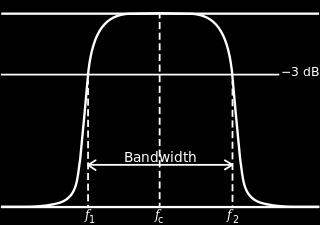
18 Cut Off Frequency 18
19 3dB Cut Off Frequency To find the LPF cut off frequency, you first need to select your cursors. You can do so by first clicking on the cursor item in your toolbar. The cursors will appear at the top of your Y-axis 1. Right-click on the green cursor arrow on your Y-axis 2. Select Set Y_Value => 3. A window pops and shows the current value of the Y- axis (in db). Subtract 3dB from this and type it in the field and click on OK 4. The cursor jumps to the cut off frequency. 5. You can select Grid by clicking on Grid Icon in Toolbar 20
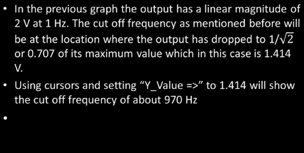
20 This LPF s cut off frequency is about 970 Hz 21


21 If instead of choosing Decibel we choose Linear for the vertical axis, the AC simulation produces the following magnitude response 21
22 22
23 23
24 DC Sweep Analysis The DC Sweep analysis generates output like that of a curve tracer. It performs a series of Operating Point analyses, modifying the voltage of a selected source in pre-defined steps, to give a DC transfer curve. DC sweep performs a sequence of DC operating point simulations. It increments the voltage or current of a selected source in predefined steps over a range of values. DC Sweep Analysis is used to calculate a circuits bias point over a range of values. This procedure allows you to simulate a circuit many times, sweeping the DC values within a predetermined range. You can control the source values by choosing the start and stop values and the increment for the DC range. The bias point of the circuit is calculated for each value of the sweep. 24
25 Multisim performs DC Sweep Analysis using the following process: 1. The DC Operating Point is calculated using a specified start value. 2. The value from the source is incremented and another DC Operating Point is calculated. 3. The increment value is added again and the process continues until the stop value is reached. 4. The result is displayed on the Grapher View. Assumptions: Capacitors are treated as open circuits, inductors as shorts. Only DC values for voltage and current sources are used.
26 In this tutorial, we will generate the i-v curve for the 1N4002 diode using Multisim. This will tell us the voltages and currents we can apply to the 1N4002 diode in the lab. Build the following circuit using 1N4002G diode in Multisim:


27 Run a DC Sweep with the following settings by going to Simulate» Analyses & Simulation» DC Sweep. Note: This will sweep the value of voltage source V1 from 0V to 1V in 1mV increments. a. Source: V1 b. Start Value: 0V c. Stop Value: 1V d. Increment: 0.001V In output tab select diode s output current, I(D1).
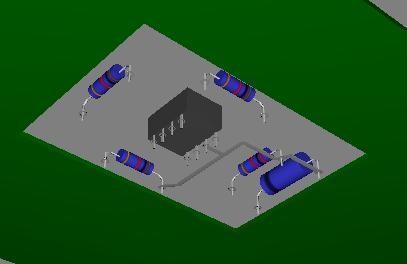
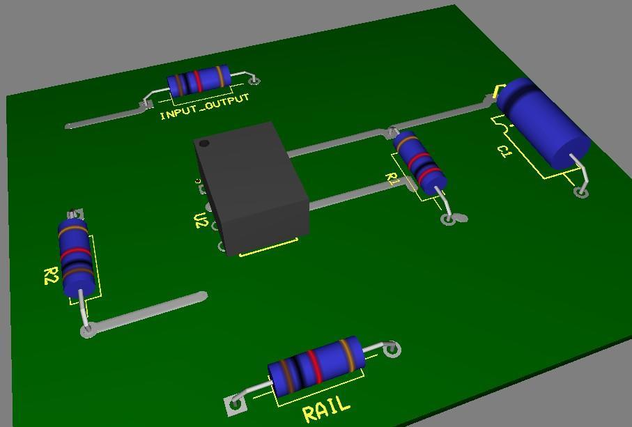
28 You should have the following typical diode i-v curve Interpret the results. Use the cursors to determine the voltage when the current equals 50mA. a. Go to Cursors» Show Cursors to show the cursors. b. Go to Cursors» Set Y Value >= to set the cursor to a specific Y value (0.05A) c. Read the corresponding X value, which should be mV in this case. Note: This means that there was a voltage drop of roughly 711mV when 50mA was flowing through the diode.
29 Plot the Reverse Bias Current. a. The plot above shows the forward i-v characteristic for the diode. b. To find the reverse i-v characteristic, simply choose a negative start value for the swept voltage. c. Set the Start Value to -101V and run the simulation again. The graph below should appear. The reverse i-v characteristic is dependent upon the peak reverse voltage of the specific diode. For the 1N4002, the peak reverse voltage is roughly 100V, which is why -101V was chosen. For another diode, this value will be different. The peak reverse voltage can be found in the specification sheet for any diode
30 Parametric Sweep The behavior of a circuit is affected when certain parameters in specific components change. With Parameter Sweep Analysis, you can verify the operation of a circuit by simulation across a range of values for a component parameter. The effect is the same as simulating the circuit several times, once for each value. You control the parameter values by choosing a start value, end value, type of sweep that you wish to simulate and the desired increment value. Parameter Sweep analysis allows you to run a series of underlying analyses, such as DC or Transient, as one or more parameters in the circuit is varied for each analysis run. This analysis is more generalized than DC Sweep.
31 Parametric Sweep Simulation of a BJT In this tutorial, we will discuss how to generate a typical I-V curve for a Bipolar Junction Transistor (BJT) in Multisim. To do this, a DC Sweep simulation will be combined with a parametric simulation. A Bipolar Junction Transistor (BJT) is a three-terminal non-linear device. Current applied to the base of the transistor (I B ) controls the amount of current that will flow from the collector to the emitter (I C ). In order to turn on the BJT device, we follow a two-step process: 1. Apply voltage across the Collector-Emitter terminals (V CE ). 2. Apply current to the base terminal (I B ). Then current (I C ) will flow from the collector to the emitter, behaving as a current source.
32 Plotting a Single I-V Curve for a BJT Build the following circuit By default, the current source (I DC ) and voltage source (V DC ) will be named I1 and V1, respectively. Rename them to I B and V CE as you see in the schematic. Make certain that the current source is upwards so current goes into the base. Set V CE = 0V and I B = 10µA. Run a DC Sweep Analysis to sweep V CE from 0V to 10V while I B pushes 10µA into the base of the transistor and observe its effect on I C. a. Set the Source to be V CE b. Start value: 0V c. Stop value: 10V d. Increment: 0.1V e. Select I C of the transistor as the output Press Run and you should see the following graph.
33 Note: This is a single I-V curve for a BJT. The x-axis is the swept variable (V CE ) and the y-axis is the collector current.

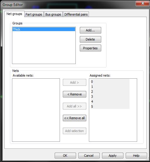
34 Plotting a Family of I-V Curves for a BJT In the simulation above, I B was fixed at 10µA while V CE was swept. Now we would like to see how the BJT behaves if both V CE and IB are swept. This is known as a DC Sweep combined with a Parametric Sweep, often called a parametric simulation. In our case, I B is the parameter we wish to vary while V CE is swept. 1. Using the same circuit from the previous simulation, reopen the DC Sweep Analysis settings. 2. Click the box next to Use source 2 to enable the second parameter I B and enter these settings. a. Set the Source to be I B b. Start value: 0A c. Stop value: 50µA (50e-6) d. Increment: 10µA (10e-6) 3. Run the simulation and the following graph should appear.
 and the y-axis is still the collector current.")
35 Note: This is called a family of I-V curves for a BJT. The x-axis is still the swept variable (V CE ) and the y-axis is still the collector current. However, now there is one I-V curve for each value of I B that we specified: 0µA, 10µA, 20µA, 30µA, 40µA, and 50µA.
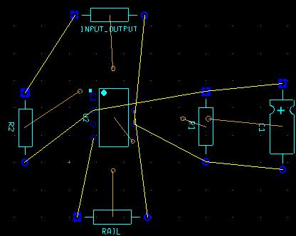
36 PCB Design in Ultiboard Now that we learned about different analysis options in Multisim, let us go back to our active low pass filter and use NI Ultiboard to make a PCB for the circuit. Before sending the schematic design from Multisim to Ultiboard we must have Footprint for all parts. (if parts are not blue, they don t have a footprint) Note: In schematic we must provision Input and Output pins to send a signal to the PCB and to measure the output. You can do this by creating in/out Jack or by using a resistor (explained later) Also the Op-amp must have a footprint associated with it 36

37 Using Resistor footprint as In/Out pins & Power Rails 37
38 As we mentioned all the BLUE color components have a footprint associated with them. Here ground is in BLACK We must create a jumper pin for it and attach pin 3 of OpAmp to it. We intentionally leave this unchanged, because we want to teach you how to manually route this pin to ground in Ultiboard. 38

39 Now we can transfer Multisim schematic to Ultiboard 39
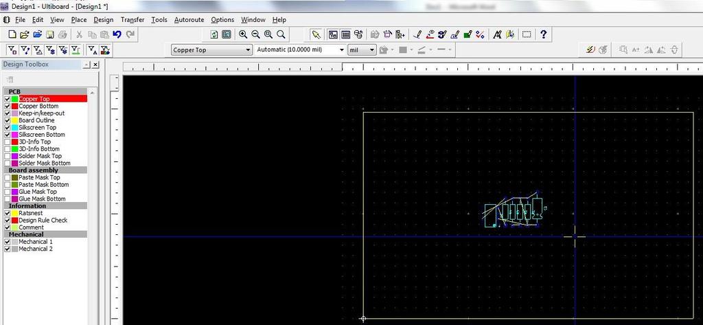
40 40

41 41


42 Changing Track width 42

43 43

44 44
45 45


46 Changing tracks from one layer to another 46

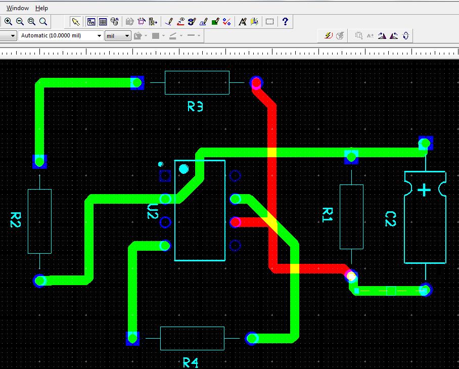
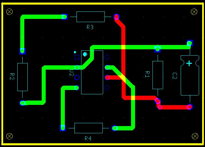
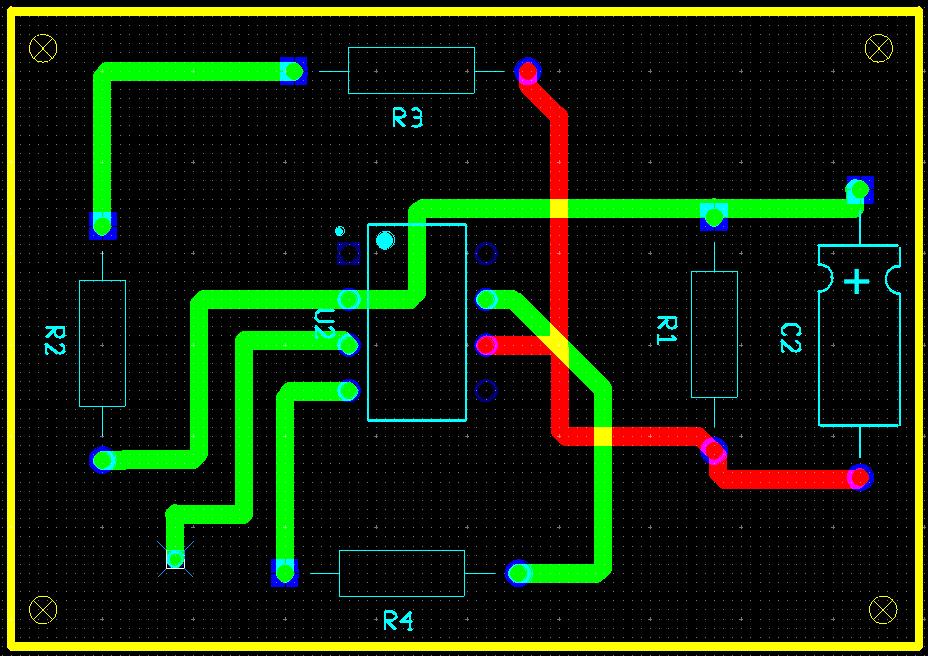
47 47


48 Creating the Board Outline 42
 to fit your PCB")
49 Double click Board Outline in PCB Design Toolbox Make sure Enable Selecting Other Objects is active Then click on the YELLOW box around your design to select it Now you can adjust this (the board outline) to fit your PCB 43
")
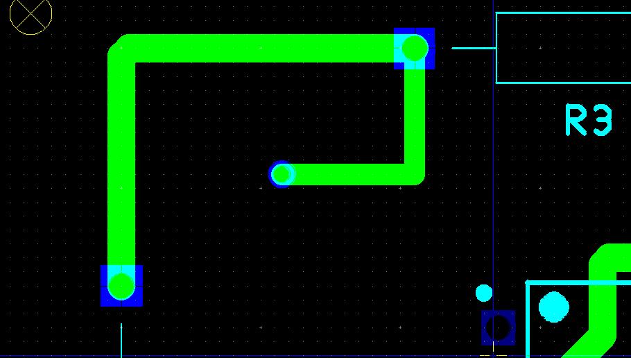
50 Design Rule Check (DRC) 44

51 3D View 51
52 52

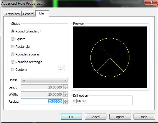
53 Placing Mounting Holes 53
54 54
55 55

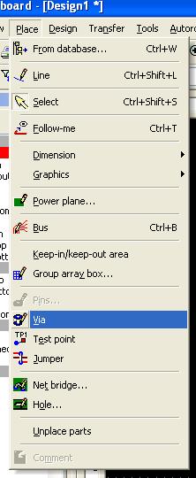
56 How to Manually Route a Trace 1. Choose a copper layer. 2. Select or enter the desired trace size in the Draw Settings toolbar. 3. Choose Place»Line. 4. Click a pad on the board. The net the pad is a part of is highlighted, and the pads in the net are each marked with an X. 5. Make your way to the next pad in the net remember to avoid parts and other traces. Click to fix the trace to the board each time you change direction. 56

57 57

58 58
59 59

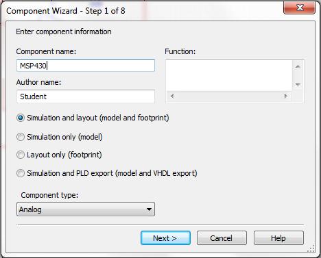
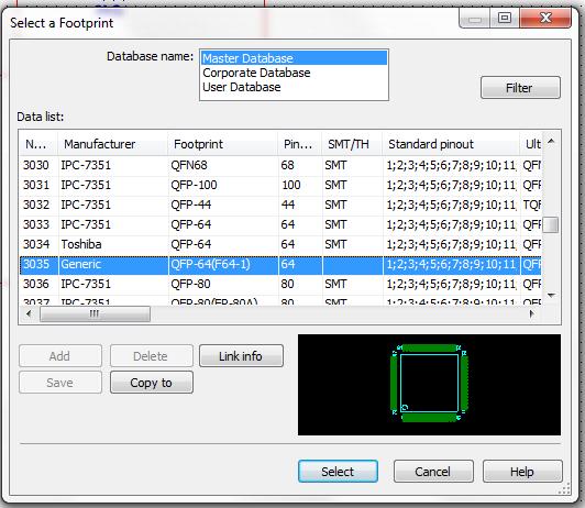
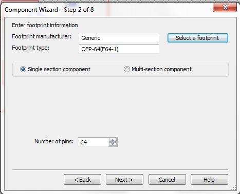
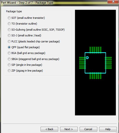
60 Now change Copper Top layer to Copper Bottom layer by highlighting it on Design Toolbox on the left hand side of the page 60

61 Choose Place»Line and draw a track connecting the VIA to the desired pin. 61
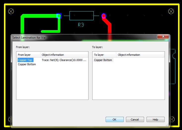
62 If you remember from earlier in Multisim we left out creating a jumper pin for GROUND Here we can manually route pin 3 of the OpAmp to create a ground Select Place Line Go on Pin3 and manually create a line (track) Route that track to a point on the corner of your PCB Add a VIA to the end (this would create a hole so you can solder a wire to it and use it as a common ground) 62

63 63

64 64
65 59

66 Creating NEW Parts in Multisim 66
67 67

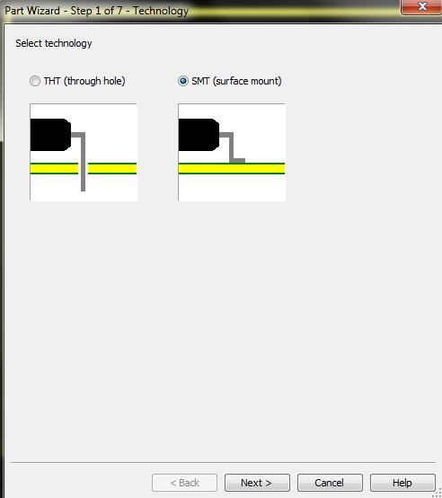
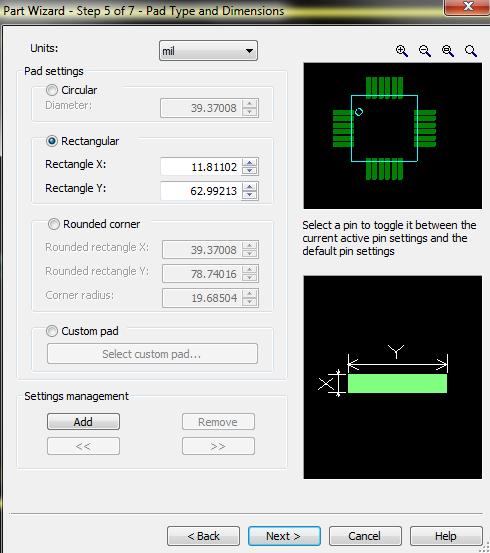
68 Creating NEW Footprint in Ultiboard 68
69 69
70 70
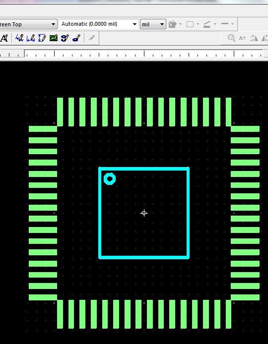
71 Suppose we want to create a footprint for our microcontroller MSP30F1611 from Texas Instrument. From MSP30F1611data sheet (or manual) we find the packaging is QFP (Quad Flat Package). 71
72 66

73 67

74 68
75 75
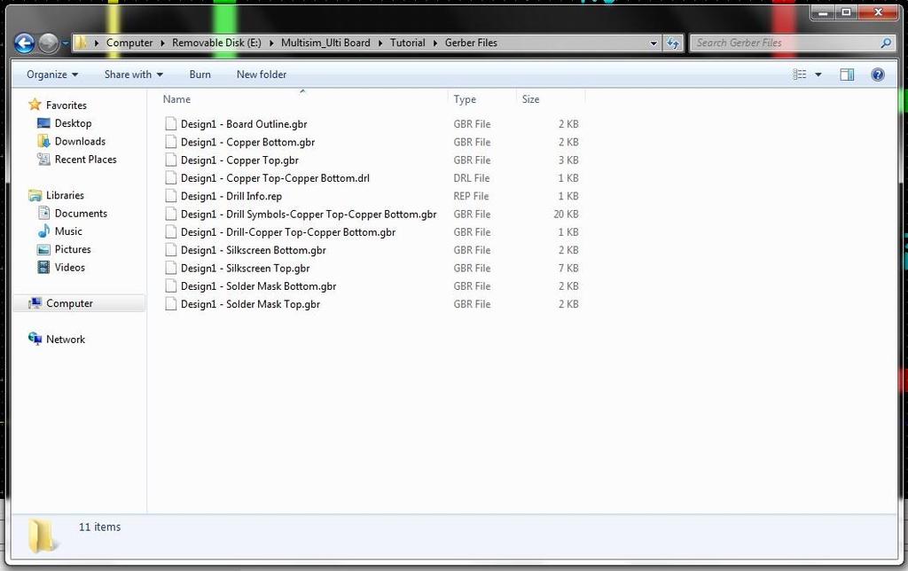
76 Exporting Gerber Files To begin generating the PCB files, the settings for each of the various file types will need to be established. The first files needed are the Gerber files which allow the manufacturer to create the basic artwork for each of the layers. From the menu: 1. Launch the Export setup window from the menu by selecting File > Export. 2. In the Export dialog box select the Gerber RS- 274X format and NC drill 76
77 77
78 In the left side of the Gerber RS-274X properties, select the following Available Layers items: 1. All copper layers (Copper Top, Copper Bottom, etc.) 2. Board Outline 3. Silkscreen Top and Silkscreen Bottom 4. Solder Mask Bottom and Solder Mask Top 5. Drill 6. Drill Symbols 78
79 It is important to complete the following steps to finalize export: In the Output units section select Imperial (inches) In the Coordinate format section, select integer 2 and decimal place 4 Click Export and your selected gerber files will be exported and saved in your designated folder 73
80 Once the save operation is completed, reorganize the files as required by the board manufacturer. Some manufacturers require the files to be zipped into a folder with a simple file naming format with just the layer names for each file type. For instance a file named SeniorDesignProject - Copper Top.gbr may need to be changed to Copper Top.gbr before sending. 80
81 78
82 1. The rep is a report file listing a summary of the drill sizes and quantities. 2. The drl file shows the exact locations of each hole. 3. In addition, there are two Gerber files that are related to PCB drilling. The Drill and Drill Symbols are created when the Gerber RS-274X is selected and subsequently these files are used in documentation such as the assembly drawing to verify all hole sizes and drill locations are correct. 4. The Drill Gerber file shows round images at each hole with the radius of the image the same as the hole radius. When viewing this layer, the user can observe the hole sizes, locations and relations to other locations on the PCB. 5. The Drill Symbols Gerber file has symbols shown for each tool. For example, if there are 5 different holes sizes needed for drilling into the PCB, there will be 5 different symbols on this Gerber layer. 82
83 Other open source software If the purpose is to create a PCB only (and no simulation is required), you can use other open source software such as 1. PCB Artist from Advanced Circuits ( 2. Eagle from CadSoft ( 83
84 Multisim User Manual: References Ultiboard User Manual:
MultiSim and Analog Discovery 2 Manual
 MultiSim and Analog Discovery 2 Manual 1 MultiSim 1.1 Running Windows Programs Using Mac Obtain free Microsoft Windows from: http://software.tamu.edu Set up a Windows partition on your Mac: https://support.apple.com/en-us/ht204009
An Introductory Guide to Circuit Simulation using NI Multisim 12
 School of Engineering and Technology An Introductory Guide to Circuit Simulation using NI Multisim 12 This booklet belongs to: This document provides a brief overview and introductory tutorial for circuit
Chapter 12: Electronic Circuit Simulation and Layout Software
 Chapter 12: Electronic Circuit Simulation and Layout Software In this chapter, we introduce the use of analog circuit simulation software and circuit layout software. I. Introduction So far we have designed
ECE4902 Lab 5 Simulation. Simulation. Export data for use in other software tools (e.g. MATLAB or excel) to compare measured data with simulation
 to compare measured data with simulation") ECE4902 Lab 5 Simulation Simulation Export data for use in other software tools (e.g. MATLAB or excel) to compare measured data with simulation Be sure to have your lab data available from Lab 5, Common
ECE4902 Lab 5 Simulation Simulation Export data for use in other software tools (e.g. MATLAB or excel) to compare measured data with simulation Be sure to have your lab data available from Lab 5, Common
ET 304A Laboratory Tutorial-Circuitmaker For Transient and Frequency Analysis
 ET 304A Laboratory Tutorial-Circuitmaker For Transient and Frequency Analysis All circuit simulation packages that use the Pspice engine allow users to do complex analysis that were once impossible to
Simulating Circuits James Lamberti 5/4/2014
 Simulating Circuits James Lamberti (jal416@lehigh.edu) 5/4/2014 There are many simulation and design platforms for circuits. The two big ones are Altium and Cadence. This tutorial will focus on Altium,
Figure AC circuit to be analyzed.
 7.2(1) MULTISIM DEMO 7.2: INTRODUCTION TO AC ANALYSIS In this section, we ll introduce AC Analysis in Multisim. This is perhaps one of the most useful Analyses that Multisim offers, and we ll use it in
PCB layout tutorial MultiSim/Ultiboard
 PCB layout tutorial MultiSim/Ultiboard The basic steps in designing a PCB Paper design and prototype of the basic circuit. Identify the parts and the footprints that will be used. Make a circuit schematic,
Introduction to PSpice
 Electric Circuit I Lab Manual 4 Session # 5 Introduction to PSpice 1 PART A INTRODUCTION TO PSPICE Objective: The objective of this experiment is to be familiar with Pspice (learn how to connect circuits,
LT Spice Getting Started Very Quickly. First Get the Latest Software!
 LT Spice Getting Started Very Quickly First Get the Latest Software! 1. After installing LT Spice, run it and check to make sure you have the latest version with respect to the latest version available
EE320L Electronics I. Laboratory. Laboratory Exercise #6. Current-Voltage Characteristics of Electronic Devices. Angsuman Roy
 EE320L Electronics I Laboratory Laboratory Exercise #6 Current-Voltage Characteristics of Electronic Devices By Angsuman Roy Department of Electrical and Computer Engineering University of Nevada, Las
Getting Started in Eagle Professional Schematic Software. Tyler Borysiak Team 9 Manager
 Getting Started in Eagle 7.3.0 Professional Schematic Software Tyler Borysiak Team 9 Manager 1 Executive Summary PCBs, or Printed Circuit Boards, are all around us. Almost every single piece of electrical
Lab 3: Very Brief Introduction to Micro-Cap SPICE
 Lab 3: Very Brief Introduction to Micro-Cap SPICE Starting Micro-Cap SPICE Micro-Cap SPICE is available on CoE machines under the Spectrum Software menu: Programs Spectrum Software Micro-Cap 10 Evaluation
Experiment #6: Biasing an NPN BJT Introduction to CE, CC, and CB Amplifiers
 SCHOOL OF ENGINEERING AND APPLIED SCIENCE DEPARTMENT OF ELECTRICAL AND COMPUTER ENGINEERING ECE 2115: ENGINEERING ELECTRONICS LABORATORY Experiment #6: Biasing an NPN BJT Introduction to CE, CC, and CB
Tutorial #5: Emitter Follower or Common Collector Amplifier Circuit
 Tutorial #5: Emitter Follower or Common Collector Amplifier Circuit This tutorial will help you to build and simulate a more complex circuit: an emitter follower. The emitter follower or common collector
Návrh, simulace a ověření elektronických obvodů na platformě NI ELVIS
 INVESTICE DO ROZVOJE VZDĚLÁVÁNÍ Návrh, simulace a ověření elektronických obvodů na platformě NI ELVIS Učební texty k semináři Autoři: Ing. Roman Vala Datum: 13. 4. 2012 Centrum pro rozvoj výzkumu pokročilých
Revised: Summer 2010
 EE 2274 PRE-LAB EXPERIMENT 5 DIODE OR GATE & CLIPPING CIRCUIT COMPLETE PRIOR TO COMING TO LAB Part I: 1. Design a diode, Figure 1 OR gate in which the maximum input current,, Iin is less than 5mA. Show
Lab 9 Frequency Domain
 Lab 9 Frequency Domain 1 Components Required Resistors Capacitors Function Generator Multimeter Oscilloscope 2 Filter Design Filters are electric components that allow applying different operations to
IME-100 ECE. Lab 1. Electrical and Computer Engineering Department Kettering University. G. Tewolde, IME100-ECE,
 IME-100 ECE Lab 1 Electrical and Computer Engineering Department Kettering University 1-1 IME-100, ECE Lab1 Circuit Design, Simulation, and Layout In this laboratory exercise, you will do the following:
Cir cuit s 212 Lab. Lab #7 Filter Design. Introductions:
 Cir cuit s 22 Lab Lab #7 Filter Design The purpose of this lab is multifold. This is a three-week experiment. You are required to design a High / Low Pass filter using the LM38 OP AMP. In this lab, you
EE 210 Lab Exercise #3 Introduction to PSPICE
 EE 210 Lab Exercise #3 Introduction to PSPICE Appending 4 in your Textbook contains a short tutorial on PSPICE. Additional information, tutorials and a demo version of PSPICE can be found at the manufacturer
A Brief Handout for Introduction to
 A Brief Handout for Introduction to Electric cal Engineering Course This handout is a compilation of PSPICE, A Brief Primer, Department of Electrical and Systems Engineering, University of Pennsylvania
Using LTspice a Short Intro with Examples
 Using LTspice a Short Intro with Examples LTspice, also called SwitcherCAD, is a powerful and easy to use schematic capture program and SPICE engine, which is a general-purpose circuit simulation program
Lab Reference Manual. ECEN 326 Electronic Circuits. Texas A&M University Department of Electrical and Computer Engineering
 Lab Reference Manual ECEN 326 Electronic Circuits Texas A&M University Department of Electrical and Computer Engineering Contents 1. Circuit Analysis in PSpice 3 1.1 Transient and DC Analysis 3 1.2 Measuring
EE 2274 DIODE OR GATE & CLIPPING CIRCUIT
 EE 2274 DIODE OR GATE & CLIPPING CIRCUIT Prelab Part I: Wired Diode OR Gate LTspice use 1N4002 1. Design a diode OR gate, Figure 1 in which the maximum current thru R1 I R1 = 9mA assume Vin = 5Vdc. Design
Class #8: Experiment Diodes Part I
 Class #8: Experiment Diodes Part I Purpose: The objective of this experiment is to become familiar with the properties and uses of diodes. We used a 1N914 diode in two previous experiments, but now we
Introduction to LT Spice IV with Examples
 Introduction to LT Spice IV with Examples 400D - Fall 2015 Purpose Part of Electronics & Control Division Technical Training Series by Nicholas Lombardo The purpose of this document is to give a basic
EEC WINTER Instructor: Xiaoguang Leo" Liu. Application Note. Baseband Design. Duyen Tran ID#: Team DMK
 EEC 134 --- WINTER 2016 Instructor: Xiaoguang Leo" Liu Application Note Baseband Design Duyen Tran ID#: 999246920 Team DMK 1 This application note provides the process to design the baseband of the radar
Introduction to OrCAD. Simulation Program With Integrated Circuits Emphasis.
 Islamic University of Gaza Faculty of Engineering Electrical Engineering department Digital Electronics Lab (EELE 3121) Eng. Mohammed S. Jouda Eng. Amani S. abu reyala Experiment 1 Introduction to OrCAD
Dr. Charles Kim ELECTRONICS I. Lab 5 Bipolar Junction Transistor (BJT) I TRADITIONAL LAB
 I TRADITIONAL LAB") ELECTRONICS I Lab 5 Bipolar Junction Transistor (BJT) I TRADITIONAL LAB MOBILE STUDIO LAB Before We Start A transistor is a 3-terminal device available in two configurations, NPN and PNP. The transistor
ELECTRONICS I Lab 5 Bipolar Junction Transistor (BJT) I TRADITIONAL LAB MOBILE STUDIO LAB Before We Start A transistor is a 3-terminal device available in two configurations, NPN and PNP. The transistor
LAB EXERCISE 3 FET Amplifier Design and Linear Analysis
 ADS 2012 Workspaces and Simulation Tools (v.1 Oct 2012) LAB EXERCISE 3 FET Amplifier Design and Linear Analysis Topics: More schematic capture, DC and AC simulation, more on libraries and cells, using
ECE 310L : LAB 9. Fall 2012 (Hay)
") ECE 310L : LAB 9 PRELAB ASSIGNMENT: Read the lab assignment in its entirety. 1. For the circuit shown in Figure 3, compute a value for R1 that will result in a 1N5230B zener diode current of approximately
ECE 310L : LAB 9 PRELAB ASSIGNMENT: Read the lab assignment in its entirety. 1. For the circuit shown in Figure 3, compute a value for R1 that will result in a 1N5230B zener diode current of approximately
EECS 312: Digital Integrated Circuits Lab Project 1 Introduction to Schematic Capture and Analog Circuit Simulation
 EECS 312: Digital Integrated Circuits Lab Project 1 Introduction to Schematic Capture and Analog Circuit Simulation Teacher: Robert Dick GSI: Shengshuo Lu Assigned: 5 September 2013 Due: 17 September 2013
Creo Revolve Tutorial
 Creo Revolve Tutorial Setup 1. Open Creo Parametric Note: Refer back to the Creo Extrude Tutorial for references and screen shots of the Creo layout 2. Set Working Directory a. From the Model Tree navigate
EK307 Active Filters and Steady State Frequency Response
 EK307 Active Filters and Steady State Frequency Response Laboratory Goal: To explore the properties of active signal-processing filters Learning Objectives: Active Filters, Op-Amp Filters, Bode plots Suggested
Name EET 1131 Lab #2 Oscilloscope and Multisim
 Name EET 1131 Lab #2 Oscilloscope and Multisim Section 1. Oscilloscope Introduction Equipment and Components Safety glasses Logic probe ETS-7000 Digital-Analog Training System Fluke 45 Digital Multimeter
.dc Vcc Ib 0 50uA 5uA
 EE 2274 BJT Biasing PreLab: 1. Common Emitter (CE) Transistor Characteristics curve Generate the characteristics curves for a 2N3904 in LTspice by plotting Ic by sweeping Vce over a set of Ib steps. Label
E B C. Two-Terminal Behavior (For testing only!) TO-92 Case Circuit Symbol
 TO-92 Case Circuit Symbol") Physics 310 Lab 5 Transistors Equipment: Little silver power-supply, little black multimeter, Decade Resistor Box, 1k,, 470, LED, 10k, pushbutton switch, 270, 2.7k, function generator, o scope, two 5.1k
Physics 310 Lab 5 Transistors Equipment: Little silver power-supply, little black multimeter, Decade Resistor Box, 1k,, 470, LED, 10k, pushbutton switch, 270, 2.7k, function generator, o scope, two 5.1k
The source component is the AC_POWER source, not AC_VOLTAGE as we ve used in previous Demos. It can be accessed under:
 8.3(1) MULTISIM DEMO 8.3: POWER FACTOR IN MULTISIM Is there a way to plot power factor in Multisim? It may not seem readily apparent, but there is in fact a way. It is rather complicated and involves some
EE 2274 RC and Op Amp Circuit Completed Prior to Coming to Lab. Prelab Part I: RC Circuit
 EE 2274 RC and Op Amp Circuit Completed Prior to Coming to Lab Prelab Part I: RC Circuit 1. Design a high pass filter (Fig. 1) which has a break point f b = 1 khz at 3dB below the midband level (the -3dB
PCB Layout. Date : 22 Dec 05. Prepare by : HK Sim Prepare by : HK Sim
 PCB Layout Date : 22 Dec 05 Main steps from Schematic to PCB Move from schematic to PCB Define PCB size Bring component from schematic to PCB Move the components to the desire position Layout the path
University of Michigan EECS 311: Electronic Circuits Fall 2008 LAB 4 SINGLE STAGE AMPLIFIER
 University of Michigan EECS 311: Electronic Circuits Fall 2008 LAB 4 SINGLE STAGE AMPLIFIER Issued 10/27/2008 Report due in Lecture 11/10/2008 Introduction In this lab you will characterize a 2N3904 NPN
PCB Design (with EAGLE tutorial) TA: Robert Likamwa ELEC 424, Fall 2010
 TA: Robert Likamwa ELEC 424, Fall 2010") PCB Design (with EAGLE tutorial) TA: Robert Likamwa ELEC 424, Fall 2010 Printed Circuit Boards What are they? How can I make one? 424 Project description Eagle Tutorial http://www.electronicmanufacturers.co.za/
PCB Design (with EAGLE tutorial) TA: Robert Likamwa ELEC 424, Fall 2010 Printed Circuit Boards What are they? How can I make one? 424 Project description Eagle Tutorial http://www.electronicmanufacturers.co.za/
The object of this experiment is to become familiar with the instruments used in the low noise laboratory.
 0. ORIENTATION 0.1 Object The object of this experiment is to become familiar with the instruments used in the low noise laboratory. 0.2 Parts The following parts are required for this experiment: 1. A
UNIVERSITY OF NORTH CAROLINA AT CHARLOTTE Department of Electrical and Computer Engineering
 UNIVERSITY OF NORTH CAROLINA AT CHARLOTTE Department of Electrical and Computer Engineering EXPERIMENT 7 BJT AMPLIFIER CONFIGURATIONS AND INPUT/OUTPUT IMPEDANCE OBJECTIVES The purpose of this experiment
ENEE207 Electric Circuits Lab Manual
 ENEE207 Electric Circuits Lab Manual Department of Engineering, Physical & Computer Sciences Montgomery College Version 3 Copyright Lan Xiang (Do not distribute without permission) 1 TABLE OF CONTENTS
ENGI0531 Lab 2 Tutorial
 ENGI0531 Lab 2 Tutorial Transient Analysis, Operating Points, Parameters and other miscellany Lakehead University Greg Toombs Winter 2009 1. Constructing the Circuit Copying a Cell View Start Cadence as
EXPERIMENT 5 CURRENT AND VOLTAGE CHARACTERISTICS OF BJT
 EXPERIMENT 5 CURRENT AND VOLTAGE CHARACTERISTICS OF BJT 1. OBJECTIVES 1.1 To practice how to test NPN and PNP transistors using multimeter. 1.2 To demonstrate the relationship between collector current
Engineering 3821 Fall Pspice TUTORIAL 1. Prepared by: J. Tobin (Class of 2005) B. Jeyasurya E. Gill
 B. Jeyasurya E. Gill") Engineering 3821 Fall 2003 Pspice TUTORIAL 1 Prepared by: J. Tobin (Class of 2005) B. Jeyasurya E. Gill 2 INTRODUCTION The PSpice program is a member of the SPICE (Simulation Program with Integrated Circuit
Engineering 3821 Fall 2003 Pspice TUTORIAL 1 Prepared by: J. Tobin (Class of 2005) B. Jeyasurya E. Gill 2 INTRODUCTION The PSpice program is a member of the SPICE (Simulation Program with Integrated Circuit
Using LTSPICE to Analyze Circuits
 Using LTSPICE to Analyze Circuits Overview: LTSPICE is circuit simulation software that automatically constructs circuit equations using circuit element models (built in or downloadable). In its modern
EXPERIMENT NUMBER 10 TRANSIENT ANALYSIS USING PSPICE
 EXPERIMENT NUMBER 10 TRANSIENT ANALYSIS USING PSPICE Objective: To learn to use a circuit simulator package for plotting the response of a circuit in the time domain. Preliminary: Revise laboratory 8 to
Gerber Setup. Modified by Susan Riege on 4-Aug Parent page: WorkspaceManager Dialogs
 Gerber Setup Modified by Susan Riege on 4-Aug-2015 Parent page: WorkspaceManager Dialogs Other Related Resources Options for Project - Options Tab (Dialog) Generate Output Files (Dialog) Aperture (Dialog)
Wheatstone Bridge. M16C Microcontroller Strain Gauge (temperature compensation)
") Overview Eagle Version: 5.11.0 Circuit: Strain gauge amplifier for interface with a microcontroller. Time Requirements 2 + 2 + 2 hours. This three part guide is intended to provide an introduction to PCB
Overview Eagle Version: 5.11.0 Circuit: Strain gauge amplifier for interface with a microcontroller. Time Requirements 2 + 2 + 2 hours. This three part guide is intended to provide an introduction to PCB
ITT Technical Institute. ET275 Electronic Communications Systems I Onsite Course SYLLABUS
 ITT Technical Institute ET275 Electronic Communications Systems I Onsite Course SYLLABUS Credit hours: 4 Contact/Instructional hours: 50 (30 Theory Hours, 20 Lab Hours) Prerequisite(s) and/or Corequisite(s):
Başkent University Department of Electrical and Electronics Engineering EEM 214 Electronics I Experiment 8. Bipolar Junction Transistor
 Başkent University Department of Electrical and Electronics Engineering EEM 214 Electronics I Experiment 8 Bipolar Junction Transistor Aim: The aim of this experiment is to investigate the DC behavior
ET275P Electronic Communications Systems I [Onsite]
![ET275P Electronic Communications Systems I [Onsite]](/thumbs/85/92760903.jpg "ET275P Electronic Communications Systems I [Onsite]") ET275P Electronic Communications Systems I [Onsite] Course Description: In this course, several methods of signal transmission and reception are covered, including such techniques as mixing, modulating
ET275P Electronic Communications Systems I [Onsite] Course Description: In this course, several methods of signal transmission and reception are covered, including such techniques as mixing, modulating
Unit WorkBook 4 Level 4 ENG U19 Electrical and Electronic Principles LO4 Digital & Analogue Electronics 2018 Unicourse Ltd. All Rights Reserved.
 Pearson BTEC Levels 4 Higher Nationals in Engineering (RQF) Unit 19: Electrical and Electronic Principles Unit Workbook 4 in a series of 4 for this unit Learning Outcome 4 Digital & Analogue Electronics
LABORATORY 2: Bridge circuits, Superposition, Thevenin Circuits, and Amplifier Circuits
 LABORATORY 2: Bridge circuits, Superposition, Thevenin Circuits, and Amplifier Circuits Note: If your partner is no longer in the class, please talk to the instructor. Material covered: Bridge circuits
Activity P55: Transistor Lab 1 The NPN Transistor as a Digital Switch (Power Output, Voltage Sensor)
") Activity P55: Transistor Lab 1 The NPN Transistor as a Digital Switch (Power Output, Voltage Sensor) Concept DataStudio ScienceWorkshop (Mac) ScienceWorkshop (Win) Semiconductors P55 Digital Switch.DS
Activity P55: Transistor Lab 1 The NPN Transistor as a Digital Switch (Power Output, Voltage Sensor) Concept DataStudio ScienceWorkshop (Mac) ScienceWorkshop (Win) Semiconductors P55 Digital Switch.DS
Getting Started with Qucs
 Getting Started with Qucs Graham Edge University of Toronto After downloading Qucs, installing it, and running for the first time you should see a window that looks something like this: The large yellow
Lecture 2 Analog circuits...or How to detect the Alarm beacon
 Lecture 2 Analog circuits..or How to detect the Alarm beacon I t IR light generates collector current V1 9V +V I c Q1 OP805 IR detection Vout Noise sources: Electrical (60Hz, 120Hz, 180Hz.) Other electrical
7. Bipolar Junction Transistor
 41 7. Bipolar Junction Transistor 7.1. Objectives - To experimentally examine the principles of operation of bipolar junction transistor (BJT); - To measure basic characteristics of n-p-n silicon transistor
Experiment P48: Transistor Lab 1 The NPN Transistor as a Digital Switch (Power Amplifier, Voltage Sensor)
") PASCO scientific Vol. 2 Physics Lab Manual: P48-1 Experiment P48: Transistor Lab 1 The NPN Transistor as a Digital Switch (Power Amplifier, Voltage Sensor) Concept Time SW Interface Macintosh file Windows
PASCO scientific Vol. 2 Physics Lab Manual: P48-1 Experiment P48: Transistor Lab 1 The NPN Transistor as a Digital Switch (Power Amplifier, Voltage Sensor) Concept Time SW Interface Macintosh file Windows
ECE 6416 Low-Noise Electronics Orientation Experiment
 ECE 6416 Low-Noise Electronics Orientation Experiment Object The object of this experiment is to become familiar with the instruments used in the low noise laboratory. Parts The following parts are required
Ansoft Designer Tutorial ECE 584 October, 2004
 Ansoft Designer Tutorial ECE 584 October, 2004 This tutorial will serve as an introduction to the Ansoft Designer Microwave CAD package by stepping through a simple design problem. Please note that there
EXPERIMENT 10: SINGLE-TRANSISTOR AMPLIFIERS 10/27/17
 EXPERIMENT 10: SINGLE-TRANSISTOR AMPLIFIERS 10/27/17 In this experiment we will measure the characteristics of the standard common emitter amplifier. We will use the 2N3904 npn transistor. If you have
EE320L Electronics I. Laboratory. Laboratory Exercise #2. Basic Op-Amp Circuits. Angsuman Roy. Department of Electrical and Computer Engineering
 EE320L Electronics I Laboratory Laboratory Exercise #2 Basic Op-Amp Circuits By Angsuman Roy Department of Electrical and Computer Engineering University of Nevada, Las Vegas Objective: The purpose of
Experiments #6. Differential Amplifier
 Experiments #6 Differential Amplifier 1) Objectives: To understand the DC and AC operation of a differential amplifier. To measure DC voltages and currents in differential amplifier. To obtain measured
LTSpice Basic Tutorial
 Index: I. Opening LTSpice II. Drawing the circuit A. Making Sure You Have a GND B. Getting the Parts C. Placing the Parts D. Connecting the Circuit E. Changing the Name of the Part F. Changing the Value
ECE 201 LAB 6 INTRODUCTION TO SPICE/PSPICE
 Version 1.1 1 of 33 BEFORE YOU BEGIN PREREQUISITE LABS Resistive Circuits EXPECTED KNOWLEDGE ECE 201 LAB 6 INTRODUCTION TO SPICE/PSPICE Ohm's Law: v = ir Node Voltage and Mesh Current Methods of Circuit
Lab 2: Discrete BJT Op-Amps (Part I)
") Lab 2: Discrete BJT Op-Amps (Part I) This is a three-week laboratory. You are required to write only one lab report for all parts of this experiment. 1.0. INTRODUCTION In this lab, we will introduce and
Lab 2: Discrete BJT Op-Amps (Part I) This is a three-week laboratory. You are required to write only one lab report for all parts of this experiment. 1.0. INTRODUCTION In this lab, we will introduce and
Experiment P49: Transistor Lab 2 Current Gain: The NPN Emitter-Follower Amplifier (Power Amplifier, Voltage Sensor)
") PASCO scientific Vol. 2 Physics Lab Manual: P49-1 Experiment P49: Transistor Lab 2 Current Gain: The NPN Emitter-Follower Amplifier (Power Amplifier, Voltage Sensor) Concept Time SW Interface Macintosh
PASCO scientific Vol. 2 Physics Lab Manual: P49-1 Experiment P49: Transistor Lab 2 Current Gain: The NPN Emitter-Follower Amplifier (Power Amplifier, Voltage Sensor) Concept Time SW Interface Macintosh
Lab 3: BJT I-V Characteristics
 1. Learning Outcomes Lab 3: BJT I-V Characteristics At the end of this lab, students should know how to theoretically determine the I-V (Current-Voltage) characteristics of both NPN and PNP Bipolar Junction
Lab 9: Operational amplifiers II (version 1.5)
") Lab 9: Operational amplifiers II (version 1.5) WARNING: Use electrical test equipment with care! Always double-check connections before applying power. Look for short circuits, which can quickly destroy
Lab 9: Operational amplifiers II (version 1.5) WARNING: Use electrical test equipment with care! Always double-check connections before applying power. Look for short circuits, which can quickly destroy
BJT Characteristics & Common Emitter Transistor Amplifier
 LAB #07 Objectives 1. To graph the collector characteristics of a transistor. 2. To measure AC and DC voltages in a common-emitter amplifier. Theory BJT A bipolar (junction) transistor (BJT) is a three-terminal
1.0 Introduction to VirtualBench
 Table of Contents 1.0 Introduction to VirtualBench... 3 1. 1 VirtualBench in the Laboratory... 3 1.2 VirtualBench Specifications... 4 1.3 Introduction to VirtualBench Getting Started Guide Lab Exercises...
EXPERIMENT 6 REPORT Bipolar Junction Transistor (BJT) Characteristics
 Characteristics") Name & Surname: ID: Date: EXPERIMENT 6 REPORT Bipolar Junction Transistor (BJT) Characteristics Objectives: 1. To determine transistor type (npn, pnp),terminals, and material using a DMM 2. To graph the
Name & Surname: ID: Date: EXPERIMENT 6 REPORT Bipolar Junction Transistor (BJT) Characteristics Objectives: 1. To determine transistor type (npn, pnp),terminals, and material using a DMM 2. To graph the
SoftRock v6.0 Builder s Notes. May 22, 2006
 SoftRock v6.0 Builder s Notes May 22, 2006 Be sure to use a grounded tip soldering iron in building the v6.0 SoftRock circuit board. The soldering iron needs to have a small tip, (0.05-0.1 inch diameter),
Integrators, differentiators, and simple filters
 BEE 233 Laboratory-4 Integrators, differentiators, and simple filters 1. Objectives Analyze and measure characteristics of circuits built with opamps. Design and test circuits with opamps. Plot gain vs.
EXPERIMENT 10: SINGLE-TRANSISTOR AMPLIFIERS 11/11/10
 EXPERIMENT 10: SINGLE-TRANSISTOR AMPLIFIERS 11/11/10 In this experiment we will measure the characteristics of the standard common emitter amplifier. We will use the 2N3904 npn transistor. If you have
Experiment 15: Diode Lab Part 1
 Experiment 15: Diode Lab Part 1 Purpose Theory Overview EQUIPMENT NEEDED: Computer and Science Workshop Interface Power Amplifier (CI-6552A) (2) Voltage Sensor (CI-6503) AC/DC Electronics Lab Board (EM-8656)
ELEG 205 Analog Circuits Laboratory Manual Fall 2016
 ELEG 205 Analog Circuits Laboratory Manual Fall 2016 University of Delaware Dr. Mark Mirotznik Kaleb Burd Patrick Nicholson Aric Lu Kaeini Ekong 1 Table of Contents Lab 1: Intro 3 Lab 2: Resistive Circuits
Figure E2-1 The complete circuit showing the oscilloscope and Bode plotter.
 Example 2 An RC network using the oscilloscope and Bode plotter In this example we use the oscilloscope and the Bode plotter in an RC circuit that has an AC source. The circuit which we will construct
FACULTY OF ENGINEERING LAB SHEET
 FACULTY OF ENGINEERING LAB SHEET CIRCUITS AND SIGNALS EEL 2186 TRIMESTER 1 (218/219) -Circuit analysis using ORCAD PSpice *Note: You will be given an assessment sheet during the lab session to be completed
5.25Chapter V Problem Set
 5.25Chapter V Problem Set P5.1 Analyze the circuits in Fig. P5.1 and determine the base, collector, and emitter currents of the BJTs as well as the voltages at the base, collector, and emitter terminals.
Lecture 2 Analog circuits. Seeing the light..
 Lecture 2 Analog circuits Seeing the light.. I t IR light V1 9V +V IR detection Noise sources: Electrical (60Hz, 120Hz, 180Hz.) Other electrical IR from lights IR from cameras (autofocus) Visible light
EK307 Passive Filters and Steady State Frequency Response
 EK307 Passive Filters and Steady State Frequency Response Laboratory Goal: To explore the properties of passive signal-processing filters Learning Objectives: Passive filters, Frequency domain, Bode plots
1. Hand Calculations (in a manner suitable for submission) For the circuit in Fig. 1 with f = 7.2 khz and a source vin () t 1.
 For the circuit in Fig. 1 with f = 7.2 khz and a source vin () t 1.") Objectives The purpose of this laboratory project is to introduce to equipment, measurement techniques, and simulations commonly used in AC circuit analysis. In this laboratory session, each student will:
Objectives The purpose of this laboratory project is to introduce to equipment, measurement techniques, and simulations commonly used in AC circuit analysis. In this laboratory session, each student will:
Page 1 of 7. Power_AmpFal17 11/7/ :14
 ECE 3274 Power Amplifier Project (Push Pull) Richard Cooper 1. Objective This project will introduce two common power amplifier topologies, and also illustrate the difference between a Class-B and a Class-AB
Field Effect Transistors
 Field Effect Transistors Purpose In this experiment we introduce field effect transistors (FETs). We will measure the output characteristics of a FET, and then construct a common-source amplifier stage,
Getting Started. Right click on Lateral Workplane. Left Click on New Sketch
 Getting Started 1. Open up PTC Pro/Desktop by either double clicking the icon or through the Start button and in Programs. 2. Once Pro/Desktop is open select File > New > Design 3. Close the Pallet window
Excel Tool: Plots of Data Sets
 Excel Tool: Plots of Data Sets Excel makes it very easy for the scientist to visualize a data set. In this assignment, we learn how to produce various plots of data sets. Open a new Excel workbook, and
Laboratory 4: Biasing of Bipolar Transistors Laboratory Exercises
 Laboratory 4: Biasing of Bipolar Transistors Laboratory Exercises INTRODUCTION Objectives In this lab, we will design and build three different bias circuits for BJT s (Bipolar Junction Transistors). In
Voltage Current and Resistance II
 Voltage Current and Resistance II Equipment: Capstone with 850 interface, analog DC voltmeter, analog DC ammeter, voltage sensor, RLC circuit board, 8 male to male banana leads 1 Purpose This is a continuation
R 1 R 2. (3) Suppose you have two ac signals, which we ll call signals A and B, which have peak-to-peak amplitudes of 30 mv and 600 mv, respectively.
 Suppose you have two ac signals, which we ll call signals A and B, which have peak-to-peak amplitudes of 30 mv and 600 mv, respectively.") 29:128 Homework Problems 29:128 Homework 0 reference: Chapter 1 of Horowitz and Hill (1) In the circuit shown below, V in = 9 V, R 1 = 1.5 kω, R 2 = 5.6 kω, (a) Calculate V out (b) Calculate the power
29:128 Homework Problems 29:128 Homework 0 reference: Chapter 1 of Horowitz and Hill (1) In the circuit shown below, V in = 9 V, R 1 = 1.5 kω, R 2 = 5.6 kω, (a) Calculate V out (b) Calculate the power
OrCAD PSpice - Tutorial. TA: 黃玉龍
 OrCAD PSpice - Tutorial TA: 黃玉龍 r9994320@ntu.edu.tw Outline 2 Introduction Preparation Schematic Simulation Conclusion Introduction 3 OrCAD PSpice is developed by Cadence Analog circuit simulation tool
Getting Started. with Easy Blue Print
 Getting Started with Easy Blue Print User Interface Overview Easy Blue Print is a simple drawing program that will allow you to create professional-looking 2D floor plan drawings. This guide covers the
IEEE #: March 24, Rev. A
 Texas Tech University Electrical Engineering Department IEEE Student Branch Milling Tutorial An EE s Guide to Using the Milling Machine Written by: Juan Jose Chong Photos by: David Hawronsky IEEE #: 90499216
Circuit Shop v December 2003 Copyright Cherrywood Systems. All rights reserved.
 Circuit Shop v2.02 - December 2003 Copyright 1997-2003 Cherrywood Systems. All rights reserved. This manual is a printable version of Circuit Shop's help file. There are two parts to the manual: The first
Section One: Using Control Blocks for PID Controllers
 Section One: Using Control Blocks for PID Controllers In this section, the use of control blocks will be used to compensate for a Plant Given by the transfer function: Open a new Simplorer, rename the