FPGA Circuits. na A simple FPGA model. nfull-adder realization
|
|
|
- Justin Small
- 5 years ago
- Views:
Transcription
1 FPGA Circuits na A simple FPGA model nfull-adder realization ndemos
2 Presentation References n Altera Training Course Designing With Quartus-II n Altera Training Course Migrating ASIC Designs to FPGA n Altera Training Course Introduction to Verilog n S. Brown and J. Rose, Architecture of FPGAs and CPLDs: : A Tutorial, Department of Electrical and Computer Engineering, University of Toronto n Online academic notes pld devices.pdf
3 What are Programmable Chips? n As compared to hard-wired chips, programmable chips can be customized as per needs of the user by programming n This convenience, coupled with the option of re-programming in case of problems, makes the programmable chips very attractive n Other benefits include instant turnaround, low starting cost and low risk
4 What are Programmable Chips? n As compared to programmable chips, ASIC (Application Specific Integrated Circuit) has a longer design cycle and costlier ECO (Engineering Change Order) n Still, ASIC has its own market due to the added benefit of faster performance and lower cost if produced in high volume n Programmable chips are good for medium to low volume products. If I you need more than 10,000 chips, go for ASIC or hard copy
5 What is Available? n PLA (Programmable Logic Array) is a simple field programmable chip that has an AND plane followed by an OR plane. It is based on the fact that any logical function can be written in SOP (Sum of Products) form thus any function can be implemented by AND gates generating products which feed to an OR gate that sums them up
6 Example n F(A,B,C) = A B C + AB C + ABC n How will it be implemented in a PLA?
7 What is Available? n CPLD (Complex Programmable Logic Device) consists of multiple PLA blocks that are interconnected to realize larger digital systems n FPGA (Field Programmable Gate Array) has narrower logic choices and more memory elements. LUT (Lookup Table) may replace actual logic gates
8 Lookup Table n A LUT (Lookup table) is a one bit wide memory array n A 4-input 4 AND gate is replaced by a LUT that has four address inputs and one single bit output with 16 one bit locations n Location 15 would have a logic value 1 stored, all others would d be zero n LUT s can be programmed and reprogrammed to change the logical function implemented
9 LUT FOR 4-INPUT 4 EVEN PARITY GENERATOR ADDRESS ADDRESS (BINARY) CONTENTS SEMICON 1111 IC Design 0 Training Center
10 LUT in a CLB
11 PLD Design Flow Design Specification Design Entry/RTL Coding - Behavioral or Structural Description of Design LE M4K M512 I/O RTL Simulation - Functional Simulation - Verify Logic Model & Data Flow (No Timing Delays) Synthesis - Translate Design into Device Specific Primitives - Optimization to Meet Required Area & Performance Constraints Place & Route - Map Primitives to Specific Locations inside Target Technology with Reference to Area & Performance Constraints - Specify Routing Resources to Be Used
12 PLD Design Flow t clk Timing Analysis - Verify Performance Specifications Were Met - Static Timing Analysis Gate Level Simulation - Timing Simulation - Verify Design Will Work in Target Technology PC Board Simulation & Test - Simulate Board Design - Program & Test Device on Board
13 Why FPGA? n FPGA chips handle dense logic and memory elements offering very high logic capacity n Uncommitted logic blocks are replicated in an FPGA with interconnects and I/O blocks
14 FPGA
15 Manufacturers and types of FPGAs n Quick Logic n Actel n Altera n Atmel n DynaChip n Lucent n Motorola n Vantis n Xilinx n Gate Field n I-Cube n Lattix n Aptix n Antifuse-FPGA n SRAM-FPGA n Flash-FPGA FPGA n FPIDs

16 Altera s FPGA Layout


17 Meet Altera: Our Industry Contact Programmable Devices Design Software Intellectual Property (IP)
18 Introduction to Altera Devices n Programmable Logic Families High & Medium Density FPGAs» Stratix II, Stratix, APEX II, APEX 20K, & FLEX 10K Low-Cost FPGAs» Cyclone & ACEX 1K FPGAs with Clock Data Recovery» Stratix GX & Mercury CPLDs» MAX 7000 & MAX 3000 Embedded Processor Solutions» Nios, Excalibur T Configuration Devices» EPC

19 Introduction to Altera Design Software n Software & Development Tools: Quartus II» Stratix II, Stratix, Stratix GX, Cyclone, APEX II, APEX 20K/E/C, Excalibur, & Mercury Devices» FLEX 10K/A/E, ACEX 1K, FLEX 6000, MAX 7000S/AE/B, MAX 3000A Devices Quartus II Web Edition» Free Version» Not All Features & Devices Included MAX+PLUS II» All FLEX, ACEX, & MAX Devices
20 Altera University Program n Under our membership contract, we subscribe to Quartus design software and serve its three floating licenses n The number of licenses will be increased based on growth in usage n Altera plans to send us Cyclone FPGA programming boards and a few w FPGA chips n Cyclone is the lowest cost FPGA family ($3-$7 $7 per chip) and includes maximum of 20K logic elements and 300Kbits of memory n Stratix is the highest density FPGA with max of 80K logic elements, 10Mbits memory, PLL, DSP and DDR interface blocks
21 Quartus II Development System n Fully-Integrated Design Tool n Multiple Design Entry Methods n Logic Synthesis n Place & Route n Simulation n Timing & Power Analysis n Device Programming
22 More Features n MegaWizard & SOPC Builder Design Tools n LogicLock Optimization Tool n NativeLink 3 rd -Party EDA Tool Integration n Integrated Embedded Software Development n SignalTap II & SignalProbe Debug Tools n Windows, Solaris, HPUX, & Linux Support n Node-Locked & Network Licensing Options n Revision Control Interface
23 Nios: : The processor in software n Altera has implemented a full 16/32 bit RISC processor in HDL (Hardware Description Language) n Nios is a processor core that is available as a megafunction in Quartus and it can be targeted for all Altera FPGA s n Programs can be written for Nios using open GNU pro tools
24 Megafunctions n Pre-Made Design Blocks Ex. Multiply-Accumulate, PLL, Double-Data Data Rate, Nios n Benefits Accelerate Design Entry Pre-Optimized for Altera Architecture Add Flexibility n Two Types Altera-Specific Megafunctions Library of Paramerterized Modules (LPMs( LPMs)» Industry Standard Logic Functions


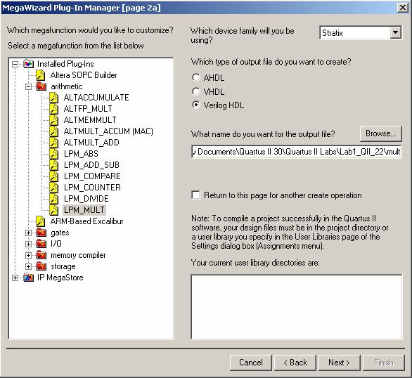
25 MegaWizard Plug-In Manager n Eases Implementation of Megafunctions & IP
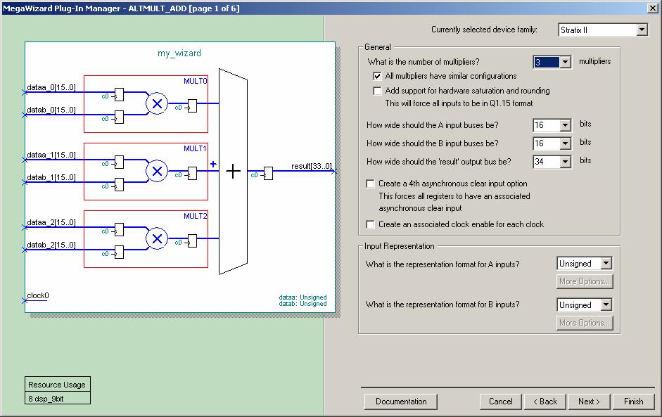
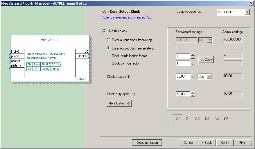
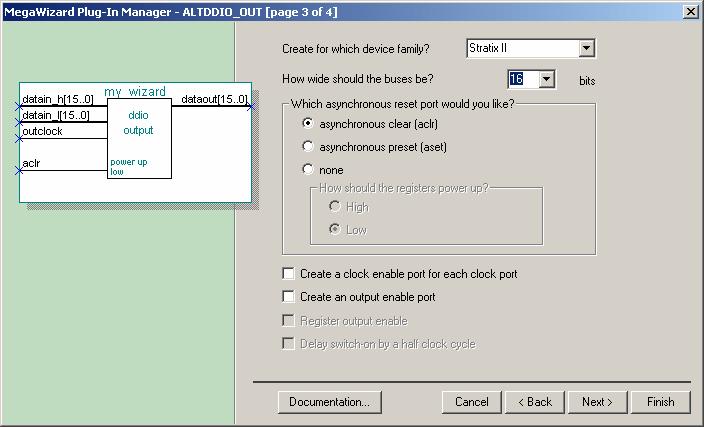
26 MegaWizard Examples Multiply-Add PLL Double-Data Rate
27 FPGA Design Cycle with Altera Quartus Tool n Define a new project and enter the design using VHDL, Verilog or AHDL languages. Design can also be entered using Schematic diagrams that can be translated to any HDL n Compile and simulate the design. Find and fix timing violations. Get power consumption estimates and perform synthesis n Download the design to FPGA using a programmer board
28 Downloading the Design n Once we verify FPGA based design, the design tool allows us to download the program to an FPGA chip n Designs can be downloaded using parallel port or USB cables n Designs can also be downloaded via the Internet to a target device
29 Downloading the Design
30 Hard Copy n Once an FPGA design is verified, validated and used successfully, there is an option to migrate it to structured ASIC n This option is known as Hard Copy n Using hard copy, FPGA design can be migrated to hard-wired design removing all configuration circuitry and programmability so that the target chip can be produced in high volume n Hard copied chip uses 40% less power than FPGA and the internal delays are reduced
31 A simple FPGA model n The abstract FPGA device is made up of a regular two-dimensional array of cells n Each cell has four faces n Signals can connect the face of the tile and can be individually configured for input or output
32 FPGA structure n Additionally to the previous array express buses are needed n The most modern FPGA architectures provide some kind of special long distance routing n The cell architecture is comprised of a function unit that can assume any two input logic function, a 2:1 multiplexer, or a D-type flip-flop n Reset and clear signals are routed to each cell n The function unit can also implement an inverter as well as the identity function
33 Logic functions n In principle: the function unit could realize any three input logic function n However: it is not very common for current FPGAs to provide cells with such three input functions although some do allow two 2-input gates to be realised with separate outputs n Cells which can realize 2:1 multiplexers are becoming more widespread this is the only kind of three input function that we allow n In practise: the third signal will come not from a neighbouring cell but from a local or global express bus signal
34 Cell level connections n Each output port can be driven by the output of the function unit or an input from any other face
35 Full-adder n Signal flow through full-adder
36 Full-adder made up of half-adders adders
37 Implementation of the half-adder adder n (a) half-adder adder top level n (b) implementation
38 Gate level topology of full-adder
39 A full-adder realization I n The circuit adds A and B with carry in to produce sum and carry out n The B input is split into two paths by the bottom left cell
40 A full-adder realization II n This can be done by realizing the identity function in the cell and connecting the South and West ports to the cell s function unit output n Both exclusive-or gates take their inputs from the North and East ports and deliver the exclusive-or of these inputs on the West face n The South port of these cells is connected to the North input (shown as a grey line) allowing the carry in to be propagated to the cell below
41 FPGA /ATMEL/ 6000 series Features n High-performance n Up to 204 User I/Os n Thousands of Registers n Cache Logic Design n Low Voltage and Standard Voltage Operation n Automatic Component Generators n Very Low-power Consumption n Programmable Clock Options n Independently Configurable I/O (PCI Compatible) n Easy Migration to Atmel Gate Arrays for High Volume Production
42 FPGA /ATMEL/ 6000 series n AT6000 Series SRAM-Based Field Programmable Gate Arrays (FPGAs) are ideal for use as reconfigurable coprocessors and implementing compute intensive logic n Supporting system speeds greater than 100 MHz and using a typical operating current of 15 to 170 ma, AT6000 Series devices are ideal for high-speed, compute-intensive designs n The patented AT6000 Series architecture employs a symmetrical grid of small yet powerful cells connected to a flexible busing network. Independently controlled clocks and resets govern every column of cells n The array is surrounded by programmable I/O
43 FPGA /ATMEL/ 6000 series n Devices range in size from 4,000 to 30,000 usable gates, and 1024 to 6400 registers. Pin locations are consistent throughout the AT6000 Series for easy design migration n AT6000 Series FPGAs utilize a reliable 0.6 mm single poly, double- metal CMOS process and are 100% factory tested n The cell s small size leads to arrays with large numbers of cells, greatly multiplying the functionality in each cell n A simple, high-speed busing network provides fast, efficient communication over medium and long distances.
44 ATMEL 6000 /The Symmetrical Array n At the heart of the Atmel architecture is a symmetrical array of identical cells n The array is continuous and completely uninterrupted from one edge to the other, except for bus repeaters spaced every eight cells n In addition to logic and storage, cells can also be used as wires to connect functions together over short distances and are useful for routing in tight spaces
45 ATMEL 6000 /The Busing Network n There are two kinds of buses: local and express n Local buses are the link between the array of cells and the busing network n There are two local buses North-South 1 and 2 for every column of cells, and two local buses East-West 1 and 2 for every row of cells n Express buses are not connected directly to cells, and thus provide higher speeds n They are the fastest way to cover long, straight-line distances within the array n Each express bus is paired with a local bus, so there are two express buses for every column and two express buses for every row of cells
46 ATMEL 6000 /The Cell Structure n The Atmel cell can be programmed to perform all the logic and wiring functions needed to implement any digital circuit n To read a local bus, the pass gate for that bus is turned on and the three input multiplexer is set accordingly n To write to a local bus, the pass gate for that bus and the pass gate for the associated tristate driver are both turned on n The operations of reading, writing and turning are subject to the restriction that each bus can be involved in no more than a single operation Reference:
47 ATMEL AVR Modules The Development environment is composed of: n The main board Including Atmel AVR microcontroller Its types:» Atmel Atmega128/64 development main board» Atmel Atmega16/32 development main board» Atmel Atmega8 development main board» Atmel Attiny15L development main board n Peripherals They can be connected with standard strip line to the main board
 - 2 Slices - 2 Logic Cells - 2 Look-up tables with 4 inputs, 2 flip-flops, flops, carry logic and")
48 Xilinx: SRAM-FPGA n Several times reprogrammable n Xilinx Virtex Architecture: n Consisting of more than 10mio cells n 1 module consisting of: - I/O-Blocks (IOB) - Block-Select Select-RAM - Combinatorial Logic Blocks (CLB) - 2 Slices - 2 Logic Cells - 2 Look-up tables with 4 inputs, 2 flip-flops, flops, carry logic and routing
49 Schematic circuit of a slice:
50 LUT Look-up table n Programmed part of CLB n 4 Inputs, 1 Output n Each LUT contains 16x1 Bit memory n Conditioned to give for each combination at the input a value of a logic function at the output n Get the program at Switch-ON from Block-RAM n Program is erased after Switch-OFF
 and Combinatorial cells")
51 Actel: Antifuse-FPGA n Only once programmable n Need less currency than SRAM-FPGAs n Actel SX-Architecture: n Built out of different metal-layers layers n Connections are set during first programming n Connections cannot be changed n 1 module consisting of: - Superclusters - 2 Clusters - 3 logic cells: Register-cells (R-cells) and Combinatorial cells (C-cells)
52 Construction in particular: n R- and C-cells C organized in horizontal banks: Clusters n 2 types of clusters: Type 1: 2 C-cells, C 1 R-cellR Type 2: 1 C-cell, C 2 R-cellsR n 2 types of superclusters: Type 1: 2 type-1-clusters Type 2: 1 type-1-cluster and 1 type-2-cluster n More type-1-superclusters existing because more combinatorial logic is needed

53 Pictures of antifuses: Conducting Not conducting Schematic picture of superclusters
54 Conclusion: SRAM or Antifuse? Main differences: - Susceptible for radiation SRAM - Reprogrammable - Need more currency - No hot-swapping - Not reprogrammable - Need less currency - Resistant against radiation - Hot-swapping Antifuse

55 In general: Regarding to intention n E.g: electric system for satellites: Radiation Errors can appear in SRAM-FPGAs System-update might be necessary Hot-swapping swapping-ability ability better 2 Solutions:
56 Presentations (Demos) n Xilinx demo Older, but informative n Simplify demo Newer n LabView FPGA at the National Instruments On-line demo With built-in in movies
PE713 FPGA Based System Design
 PE713 FPGA Based System Design Why VLSI? Dept. of EEE, Amrita School of Engineering Why ICs? Dept. of EEE, Amrita School of Engineering IC Classification ANALOG (OR LINEAR) ICs produce, amplify, or respond
Reference. Wayne Wolf, FPGA-Based System Design Pearson Education, N Krishna Prakash,, Amrita School of Engineering
 FPGA Fabrics Reference Wayne Wolf, FPGA-Based System Design Pearson Education, 2004 CPLD / FPGA CPLD Interconnection of several PLD blocks with Programmable interconnect on a single chip Logic blocks executes
Lecture 3, Handouts Page 1. Introduction. EECE 353: Digital Systems Design Lecture 3: Digital Design Flows, Simulation Techniques.
 Introduction EECE 353: Digital Systems Design Lecture 3: Digital Design Flows, Techniques Cristian Grecu grecuc@ece.ubc.ca Course web site: http://courses.ece.ubc.ca/353/ What have you learned so far?
FPGA Based System Design
 FPGA Based System Design Reference Wayne Wolf, FPGA-Based System Design Pearson Education, 2004 Why VLSI? Integration improves the design: higher speed; lower power; physically smaller. Integration reduces
CHAPTER III THE FPGA IMPLEMENTATION OF PULSE WIDTH MODULATION
 34 CHAPTER III THE FPGA IMPLEMENTATION OF PULSE WIDTH MODULATION 3.1 Introduction A number of PWM schemes are used to obtain variable voltage and frequency supply. The Pulse width of PWM pulsevaries with
ACEX 1K. Features... Programmable Logic Device Family. Tools
 ACEX 1K Programmable Logic Device Family May 2003, ver. 3.4 Data Sheet Features... Programmable logic devices (PLDs), providing low cost system-on-a-programmable-chip (SOPC) integration in a single device
ACEX 1K. Features... Programmable Logic Family. Tools. Table 1. ACEX TM 1K Device Features
 ACEX 1K Programmable Logic Family March 2000, ver. 1 Data Sheet Features... Programmable logic devices (PLDs), providing low cost system-on-a-programmable-chip integration in a single device Enhanced embedded
FLEX 10KE. Features... Embedded Programmable Logic Device
 FLEX 10KE Embedded Programmable Logic Device January 2003, ver. 2.5 Data Sheet Features... Embedded programmable logic devices (PLDs), providing system-on-a-programmable-chip (SOPC) integration in a single
PROGRAMMABLE ASICs. Antifuse SRAM EPROM
 PROGRAMMABLE ASICs FPGAs hold array of basic logic cells Basic cells configured using Programming Technologies Programming Technology determines basic cell and interconnect scheme Programming Technologies
FLEX 10K. Features... Embedded Programmable Logic Family. Table 1. FLEX 10K Device Features
 FLEX 10K Embedded Programmable Logic Family May 1998, ver. 3.10 Data Sheet Features... The industryõs first embedded programmable logic device (PLD) Table 1. FLEX 10K Device Features Feature Typical gates
Digital Systems Design
 Digital Systems Design Digital Systems Design and Test Dr. D. J. Jackson Lecture 1-1 Introduction Traditional digital design Manual process of designing and capturing circuits Schematic entry System-level
WHAT ARE FIELD PROGRAMMABLE. Audible plays called at the line of scrimmage? Signaling for a squeeze bunt in the ninth inning?
 WHAT ARE FIELD PROGRAMMABLE Audible plays called at the line of scrimmage? Signaling for a squeeze bunt in the ninth inning? They re none of the above! We re going to take a look at: Field Programmable
FLEX 10K. Features... Embedded Programmable Logic Family. Preliminary Information
 FLEX 10K Embedded Programmable Logic Family June 1996, ver. 2 Data Sheet Features... The industry s first embedded programmable logic device (PLD) family, providing system integration in a single device
Implementing Logic with the Embedded Array
 Implementing Logic with the Embedded Array in FLEX 10K Devices May 2001, ver. 2.1 Product Information Bulletin 21 Introduction Altera s FLEX 10K devices are the first programmable logic devices (PLDs)
Digital Systems Design
 Digital Systems Design Clock Networks and Phase Lock Loops on Altera Cyclone V Devices Dr. D. J. Jackson Lecture 9-1 Global Clock Network & Phase-Locked Loops Clock management is important within digital
Techniques for Implementing Multipliers in Stratix, Stratix GX & Cyclone Devices
 Techniques for Implementing Multipliers in Stratix, Stratix GX & Cyclone Devices August 2003, ver. 1.0 Application Note 306 Introduction Stratix, Stratix GX, and Cyclone FPGAs have dedicated architectural
APPLICATION OF PROGRAMMABLE LOGIC DEVICES FOR ACQUISITION OF ECG SIGNAL WITH PACEMAKER PULSES 1. HISTORY OF PROGRAMMABLE CIRCUITS
 JOURNAL OF MEDICAL INFORMATICS & TECHNOLOGIES Vol.4/2002, ISSN 1642-6037 Leszek DREWNIOK *, Janusz ZMUDZINSKI *, Jerzy GALECKA *, Adam GACEK * programmable circuits ECG acquisition with cardiostimulator
Technology Timeline. Transistors ICs (General) SRAMs & DRAMs Microprocessors SPLDs CPLDs ASICs. FPGAs. The Design Warrior s Guide to.
 SRAMs & DRAMs Microprocessors SPLDs CPLDs ASICs. FPGAs. The Design Warrior s Guide to.") FPGAs 1 CMPE 415 Technology Timeline 1945 1950 1955 1960 1965 1970 1975 1980 1985 1990 1995 2000 Transistors ICs (General) SRAMs & DRAMs Microprocessors SPLDs CPLDs ASICs FPGAs The Design Warrior s Guide
FPGAs 1 CMPE 415 Technology Timeline 1945 1950 1955 1960 1965 1970 1975 1980 1985 1990 1995 2000 Transistors ICs (General) SRAMs & DRAMs Microprocessors SPLDs CPLDs ASICs FPGAs The Design Warrior s Guide
Engr354: Digital Logic Circuits
 Engr354: Digital Logic Circuits Chapter 3: Implementation Technology Curtis Nelson Chapter 3 Overview In this chapter you will learn about: How transistors are used as switches; Integrated circuit technology;
2009 Spring CS211 Digital Systems & Lab 1 CHAPTER 3: TECHNOLOGY (PART 2)
") 1 CHAPTER 3: IMPLEMENTATION TECHNOLOGY (PART 2) Whatwillwelearninthischapter? we learn in this 2 How transistors operate and form simple switches CMOS logic gates IC technology FPGAs and other PLDs Basic
1 CHAPTER 3: IMPLEMENTATION TECHNOLOGY (PART 2) Whatwillwelearninthischapter? we learn in this 2 How transistors operate and form simple switches CMOS logic gates IC technology FPGAs and other PLDs Basic
Using Soft Multipliers with Stratix & Stratix GX
 Using Soft Multipliers with Stratix & Stratix GX Devices November 2002, ver. 2.0 Application Note 246 Introduction Traditionally, designers have been forced to make a tradeoff between the flexibility of
Design Methodologies. Digital Integrated Circuits A Design Perspective. Jan M. Rabaey Anantha Chandrakasan Borivoje Nikolic.
 Digital Integrated Circuits A Design Perspective Jan M. Rabaey Anantha Chandrakasan Borivoje Nikolic Design Methodologies December 10, 2002 L o g i c T r a n s i s t o r s p e r C h i p ( K ) 1 9 8 1 1
PROGRAMMABLE ASIC INTERCONNECT
 PROGRAMMABLE ASIC INTERCONNECT The structure and complexity of the interconnect is largely determined by the programming technology and the architecture of the basic logic cell The first programmable ASICs
Arria V Timing Optimization Guidelines
 Arria V Timing Optimization Guidelines AN-652-1. Application Note This document presents timing optimization guidelines for a set of identified critical timing path scenarios in Arria V FPGA designs. Timing
FPGA-Based Autonomous Obstacle Avoidance Robot.
 People s Democratic Republic of Algeria Ministry of Higher Education and Scientific Research University M Hamed BOUGARA Boumerdes Institute of Electrical and Electronic Engineering Department of Electronics
Chapter 4 Combinational Logic Circuits
 Chapter 4 Combinational Logic Circuits Chapter 4 Objectives Selected areas covered in this chapter: Converting logic expressions to sum-of-products expressions. Boolean algebra and the Karnaugh map as
ECE380 Digital Logic
 ECE380 Digital Logic Implementation Technology: Standard Chips and Programmable Logic Devices Dr. D. J. Jackson Lecture 10-1 Standard chips A number of chips, each with a few logic gates, are commonly
Method We follow- How to Get Entry Pass in SEMICODUCTOR Industries for 2 nd year engineering students
 Method We follow- How to Get Entry Pass in SEMICODUCTOR Industries for 2 nd year engineering students FIG-2 Winter/Summer Training Level 1 (Basic & Mandatory) & Level 1.1 continues. Winter/Summer Training
Chapter 4 Combinational Logic Circuits
 Chapter 4 Combinational Logic Circuits Chapter 4 Objectives Selected areas covered in this chapter: Converting logic expressions to sum-of-products expressions. Boolean algebra and the Karnaugh map as
Design Methodologies. Digital Integrated Circuits A Design Perspective. Jan M. Rabaey Anantha Chandrakasan Borivoje Nikolic.
 Digital Integrated Circuits A Design Perspective Jan M. Rabaey Anantha Chandrakasan Borivoje Nikolic Design Methodologies December 10, 2002 L o g i c T r a n s i s t o r s p e r C h i p ( K ) 1 9 8 1 1
Digital design & Embedded systems
 FYS4220/9220 Digital design & Embedded systems Lecture #5 J. K. Bekkeng, 2.7.2011 Phase-locked loop (PLL) Implemented using a VCO (Voltage controlled oscillator), a phase detector and a closed feedback
ASIC Implementation and Analysis of Extrinsic EHW Based Power and Area Optimised 8-Bit Asynchronous Parallel MAC
 266 ASIC Implementation and Analysis of Extrinsic EHW Based Power and Area Optimised 8-Bit Asynchronous Parallel MAC D.Dhanasekaran, and **Dr.K.Boopathy Bagan *Assistant Professor, SVCE, Pennalur,Sriperumbudur-602105.
Stratix II Filtering Lab
 October 2004, ver. 1.0 Application Note 362 Introduction The filtering reference design provided in the DSP Development Kit, Stratix II Edition, shows you how to use the Altera DSP Builder for system design,
Journal of Engineering Science and Technology Review 9 (5) (2016) Research Article. L. Pyrgas, A. Kalantzopoulos* and E. Zigouris.
 (2016) Research Article. L. Pyrgas, A. Kalantzopoulos* and E. Zigouris.") Jestr Journal of Engineering Science and Technology Review 9 (5) (2016) 51-55 Research Article Design and Implementation of an Open Image Processing System based on NIOS II and Altera DE2-70 Board L. Pyrgas,
Jestr Journal of Engineering Science and Technology Review 9 (5) (2016) 51-55 Research Article Design and Implementation of an Open Image Processing System based on NIOS II and Altera DE2-70 Board L. Pyrgas,
4. Embedded Multipliers in Cyclone IV Devices
 February 2010 CYIV-51004-1.1 4. Embedded Multipliers in Cyclone IV evices CYIV-51004-1.1 Cyclone IV devices include a combination of on-chip resources and external interfaces that help increase performance,
R Using the Virtex Delay-Locked Loop
 Application Note: Virtex Series XAPP132 (v2.4) December 20, 2001 Summary The Virtex FPGA series offers up to eight fully digital dedicated on-chip Delay-Locked Loop (DLL) circuits providing zero propagation
Programmable Interconnect. CPE/EE 428, CPE 528: Session #13. Actel Programmable Interconnect. Actel Programmable Interconnect
 Programmable Interconnect CPE/EE 428, CPE 528: Session #13 Department of Electrical and Computer Engineering University of Alabama in Huntsville In addition to programmable cells, programmable ASICs must
Stratix Filtering Reference Design
 Stratix Filtering Reference Design December 2004, ver. 3.0 Application Note 245 Introduction The filtering reference designs provided in the DSP Development Kit, Stratix Edition, and in the DSP Development
LOW-POWER SOFTWARE-DEFINED RADIO DESIGN USING FPGAS
 LOW-POWER SOFTWARE-DEFINED RADIO DESIGN USING FPGAS Charlie Jenkins, (Altera Corporation San Jose, California, USA; chjenkin@altera.com) Paul Ekas, (Altera Corporation San Jose, California, USA; pekas@altera.com)
Hardware Implementation of BCH Error-Correcting Codes on a FPGA
 Hardware Implementation of BCH Error-Correcting Codes on a FPGA Laurenţiu Mihai Ionescu Constantin Anton Ion Tutănescu University of Piteşti University of Piteşti University of Piteşti Alin Mazăre University
Lecture Perspectives. Administrivia
 Lecture 29-30 Perspectives Administrivia Final on Friday May 18 12:30-3:30 pm» Location: 251 Hearst Gym Topics all what was covered in class. Review Session Time and Location TBA Lab and hw scores to be
IMPLEMENTATION OF QALU BASED SPWM CONTROLLER THROUGH FPGA. This Chapter presents an implementation of area efficient SPWM
 3 Chapter 3 IMPLEMENTATION OF QALU BASED SPWM CONTROLLER THROUGH FPGA 3.1. Introduction This Chapter presents an implementation of area efficient SPWM control through single FPGA using Q-Format. The SPWM
Lecture 30. Perspectives. Digital Integrated Circuits Perspectives
 Lecture 30 Perspectives Administrivia Final on Friday December 15 8 am Location: 251 Hearst Gym Topics all what was covered in class. Precise reading information will be posted on the web-site Review Session
4. Embedded Multipliers in the Cyclone III Device Family
 ecember 2011 CIII51005-2.3 4. Embedded Multipliers in the Cyclone III evice Family CIII51005-2.3 The Cyclone III device family (Cyclone III and Cyclone III LS devices) includes a combination of on-chip
Classic. Feature. EPLD Family. Table 1. Classic Device Features
 Classic EPLD Family May 1999, ver. 5 Data Sheet Features Complete device family with logic densities of 300 to 900 usable gates (see Table 1) Device erasure and reprogramming with non-volatile EPROM configuration
PROGRAMMABLE ASIC INTERCONNECT
 ASICs...THE COURSE (1 WEEK) PROGRAMMABLE ASIC INTERCONNECT 7 Key concepts: programmable interconnect raw materials: aluminum-based metallization and a line capacitance of 0.2pFcm 1 7.1 Actel ACT Actel
Stratix II DSP Performance
 White Paper Introduction Stratix II devices offer several digital signal processing (DSP) features that provide exceptional performance for DSP applications. These features include DSP blocks, TriMatrix
Lecture 1. Tinoosh Mohsenin
 Lecture 1 Tinoosh Mohsenin Today Administrative items Syllabus and course overview Digital systems and optimization overview 2 Course Communication Email Urgent announcements Web page http://www.csee.umbc.edu/~tinoosh/cmpe650/
Disseny físic. Disseny en Standard Cells. Enric Pastor Rosa M. Badia Ramon Canal DM Tardor DM, Tardor
 Disseny físic Disseny en Standard Cells Enric Pastor Rosa M. Badia Ramon Canal DM Tardor 2005 DM, Tardor 2005 1 Design domains (Gajski) Structural Processor, memory ALU, registers Cell Device, gate Transistor
Cyclone II Filtering Lab
 May 2005, ver. 1.0 Application Note 376 Introduction The Cyclone II filtering lab design provided in the DSP Development Kit, Cyclone II Edition, shows you how to use the Altera DSP Builder for system
Feature EP20K30E EP20K60E EP20K100 EP20K100E EP20K160E EP20K200 EP20K200E
 APEX 20K Programmable Logic Device Family March 2004, ver. 5.1 Data Sheet Features Industry s first programmable logic device (PLD) incorporating system-on-a-programmable-chip (SOPC) integration MultiCore
Digital Design and System Implementation. Overview of Physical Implementations
 Digital Design and System Implementation Overview of Physical Implementations CMOS devices CMOS transistor circuit functional behavior Basic logic gates Transmission gates Tri-state buffers Flip-flops
Implementing Multipliers with Actel FPGAs
 Implementing Multipliers with Actel FPGAs Application Note AC108 Introduction Hardware multiplication is a function often required for system applications such as graphics, DSP, and process control. The
Design and Implementation of High Speed Carry Select Adder Korrapatti Mohammed Ghouse 1 K.Bala. 2
 IJSRD - International Journal for Scientific Research & Development Vol. 3, Issue 07, 2015 ISSN (online): 2321-0613 Design and Implementation of High Speed Carry Select Adder Korrapatti Mohammed Ghouse
Chapter 1 Introduction
 Chapter 1 Introduction 1.1 Introduction There are many possible facts because of which the power efficiency is becoming important consideration. The most portable systems used in recent era, which are
VLSI IMPLEMENTATION OF MODIFIED DISTRIBUTED ARITHMETIC BASED LOW POWER AND HIGH PERFORMANCE DIGITAL FIR FILTER Dr. S.Satheeskumaran 1 K.
 VLSI IMPLEMENTATION OF MODIFIED DISTRIBUTED ARITHMETIC BASED LOW POWER AND HIGH PERFORMANCE DIGITAL FIR FILTER Dr. S.Satheeskumaran 1 K. Sasikala 2 1 Professor, Department of Electronics and Communication
NEW** FPOA** Names associated with this field : Ideal associated characteristics
 Lecture 12 Digital Circuit Implementation Issues PLAs, PALs, ROM s, FPGA s Packaging Issues Look Up Table method Multiplexer Method RAM & ROM method Xilinx and Actel Examples of FPGA s I/O for FPGA s Comparison
Implementing Multipliers
 Implementing Multipliers in FLEX 10K Devices March 1996, ver. 1 Application Note 53 Introduction The Altera FLEX 10K embedded programmable logic device (PLD) family provides the first PLDs in the industry
Development of Software Defined Radio (SDR) Receiver
 Receiver") Journal of Engineering and Technology of the Open University of Sri Lanka (JET-OUSL), Vol.5, No.1, 2017 Development of Software Defined Radio (SDR) Receiver M.H.M.N.D. Herath 1*, M.K. Jayananda 2, 1Department
Journal of Engineering and Technology of the Open University of Sri Lanka (JET-OUSL), Vol.5, No.1, 2017 Development of Software Defined Radio (SDR) Receiver M.H.M.N.D. Herath 1*, M.K. Jayananda 2, 1Department
Digital Logic, Algorithms, and Functions for the CEBAF Upgrade LLRF System Hai Dong, Curt Hovater, John Musson, and Tomasz Plawski
 Digital Logic, Algorithms, and Functions for the CEBAF Upgrade LLRF System Hai Dong, Curt Hovater, John Musson, and Tomasz Plawski Introduction: The CEBAF upgrade Low Level Radio Frequency (LLRF) control
Design and synthesis of FPGA for speed control of induction motor
 International Journal of Physical Sciences ol. 4 (11), pp. 645-650, November, 2009 Available online at http://www.academicjournals.org/ijps ISSN 1992-1950 2009 Academic Journals Full Length Research Paper
6. DSP Blocks in Stratix II and Stratix II GX Devices
 6. SP Blocks in Stratix II and Stratix II GX evices SII52006-2.2 Introduction Stratix II and Stratix II GX devices have dedicated digital signal processing (SP) blocks optimized for SP applications requiring
Lecture 4&5 CMOS Circuits
 Lecture 4&5 CMOS Circuits Xuan Silvia Zhang Washington University in St. Louis http://classes.engineering.wustl.edu/ese566/ Worst-Case V OL 2 3 Outline Combinational Logic (Delay Analysis) Sequential Circuits
EECS 427 Lecture 21: Design for Test (DFT) Reminders
 Reminders") EECS 427 Lecture 21: Design for Test (DFT) Readings: Insert H.3, CBF Ch 25 EECS 427 F09 Lecture 21 1 Reminders One more deadline Finish your project by Dec. 14 Schematic, layout, simulations, and final
EECS 427 Lecture 21: Design for Test (DFT) Readings: Insert H.3, CBF Ch 25 EECS 427 F09 Lecture 21 1 Reminders One more deadline Finish your project by Dec. 14 Schematic, layout, simulations, and final
USING EMBEDDED PROCESSORS IN HARDWARE MODELS OF ARTIFICIAL NEURAL NETWORKS
 USING EMBEDDED PROCESSORS IN HARDWARE MODELS OF ARTIFICIAL NEURAL NETWORKS DENIS F. WOLF, ROSELI A. F. ROMERO, EDUARDO MARQUES Universidade de São Paulo Instituto de Ciências Matemáticas e de Computação
UT90nHBD Hardened-by-Design (HBD) Standard Cell Data Sheet February
 Standard Cell Data Sheet February") Semicustom Products UT90nHBD Hardened-by-Design (HBD) Standard Cell Data Sheet February 2018 www.cobham.com/hirel The most important thing we build is trust FEATURES Up to 50,000,000 2-input NAND equivalent
Semicustom Products UT90nHBD Hardened-by-Design (HBD) Standard Cell Data Sheet February 2018 www.cobham.com/hirel The most important thing we build is trust FEATURES Up to 50,000,000 2-input NAND equivalent
Propagation Delay, Circuit Timing & Adder Design. ECE 152A Winter 2012
 Propagation Delay, Circuit Timing & Adder Design ECE 152A Winter 2012 Reading Assignment Brown and Vranesic 2 Introduction to Logic Circuits 2.9 Introduction to CAD Tools 2.9.1 Design Entry 2.9.2 Synthesis
Propagation Delay, Circuit Timing & Adder Design
 Propagation Delay, Circuit Timing & Adder Design ECE 152A Winter 2012 Reading Assignment Brown and Vranesic 2 Introduction to Logic Circuits 2.9 Introduction to CAD Tools 2.9.1 Design Entry 2.9.2 Synthesis
Advanced FPGA Design. Tinoosh Mohsenin CMPE 491/691 Spring 2012
 Advanced FPGA Design Tinoosh Mohsenin CMPE 491/691 Spring 2012 Today Administrative items Syllabus and course overview Digital signal processing overview 2 Course Communication Email Urgent announcements
ERAU the FAA Research CEH Tools Qualification
 ERAU the FAA Research 2007-2009 CEH Tools Qualification Contract DTFACT-07-C-00010 Dr. Andrew J. Kornecki, Dr. Brian Butka Embry Riddle Aeronautical University Dr. Janusz Zalewski Florida Gulf Coast University
CHAPTER 4 FIELD PROGRAMMABLE GATE ARRAY IMPLEMENTATION OF FIVE LEVEL CASCADED MULTILEVEL INVERTER
 87 CHAPTER 4 FIELD PROGRAMMABLE GATE ARRAY IMPLEMENTATION OF FIVE LEVEL CASCADED MULTILEVEL INVERTER 4.1 INTRODUCTION The Field Programmable Gate Array (FPGA) is a high performance data processing general
Introduction to CMOS VLSI Design (E158) Lecture 9: Cell Design
 Lecture 9: Cell Design") Harris Introduction to CMOS VLSI Design (E158) Lecture 9: Cell Design David Harris Harvey Mudd College David_Harris@hmc.edu Based on EE271 developed by Mark Horowitz, Stanford University MAH E158 Lecture
Harris Introduction to CMOS VLSI Design (E158) Lecture 9: Cell Design David Harris Harvey Mudd College David_Harris@hmc.edu Based on EE271 developed by Mark Horowitz, Stanford University MAH E158 Lecture
Lecture 9: Cell Design Issues
 Lecture 9: Cell Design Issues MAH, AEN EE271 Lecture 9 1 Overview Reading W&E 6.3 to 6.3.6 - FPGA, Gate Array, and Std Cell design W&E 5.3 - Cell design Introduction This lecture will look at some of the
White Paper Stratix III Programmable Power
 Introduction White Paper Stratix III Programmable Power Traditionally, digital logic has not consumed significant static power, but this has changed with very small process nodes. Leakage current in digital
Mapping Multiplexers onto Hard Multipliers in FPGAs
 Mapping Multiplexers onto Hard Multipliers in FPGAs Peter Jamieson and Jonathan Rose The Edward S. Rogers Sr. Department of Electrical and Computer Engineering University of Toronto Modern FPGAs Consist
Digital Logic ircuits Circuits Fundamentals I Fundamentals I
 Digital Logic Circuits Fundamentals I Fundamentals I 1 Digital and Analog Quantities Electronic circuits can be divided into two categories. Digital Electronics : deals with discrete values (= sampled
Study of Power Consumption for High-Performance Reconfigurable Computing Architectures. A Master s Thesis. Brian F. Veale
 Study of Power Consumption for High-Performance Reconfigurable Computing Architectures A Master s Thesis Brian F. Veale Department of Computer Science Texas Tech University August 6, 1999 John K. Antonio
Open Source Digital Camera on Field Programmable Gate Arrays
 Open Source Digital Camera on Field Programmable Gate Arrays Cristinel Ababei, Shaun Duerr, Joe Ebel, Russell Marineau, Milad Ghorbani Moghaddam, and Tanzania Sewell Department of Electrical and Computer
Colour Recognizing Robot Arm Equipped with a CMOS Camera and an FPGA
 Colour Recognizing Robot Arm Equipped with a CMOS Camera and an FPGA Asma Taha Sadoon College of Engineering University of Baghdad Dina Abdul Kareem Abdul Qader College of Engineering University of Baghdad
Field Programmable Gate Array Implementation and Testing of a Minimum-phase Finite Impulse Response Filter
 Field Programmable Gate Array Implementation and Testing of a Minimum-phase Finite Impulse Response Filter P. K. Gaikwad Department of Electronics Willingdon College, Sangli, India e-mail: pawangaikwad2003
DIGITAL INTEGRATED CIRCUITS A DESIGN PERSPECTIVE 2 N D E D I T I O N
 DIGITAL INTEGRATED CIRCUITS A DESIGN PERSPECTIVE 2 N D E D I T I O N Jan M. Rabaey, Anantha Chandrakasan, and Borivoje Nikolic CONTENTS PART I: THE FABRICS Chapter 1: Introduction (32 pages) 1.1 A Historical
Field Programmable Gate Arrays based Design, Implementation and Delay Study of Braun s Multipliers
 Journal of Computer Science 7 (12): 1894-1899, 2011 ISSN 1549-3636 2011 Science Publications Field Programmable Gate Arrays based Design, Implementation and Delay Study of Braun s Multipliers Muhammad
The Application of System Generator in Digital Quadrature Direct Up-Conversion
 Communications in Information Science and Management Engineering Apr. 2013, Vol. 3 Iss. 4, PP. 192-19 The Application of System Generator in Digital Quadrature Direct Up-Conversion Zhi Chai 1, Jun Shen
Gomoku Player Design
 Gomoku Player Design CE126 Advanced Logic Design, winter 2002 University of California, Santa Cruz Max Baker (max@warped.org) Saar Drimer (saardrimer@hotmail.com) 0. Introduction... 3 0.0 The Problem...
Single Chip FPGA Based Realization of Arbitrary Waveform Generator using Rademacher and Walsh Functions
 IEEE ICET 26 2 nd International Conference on Emerging Technologies Peshawar, Pakistan 3-4 November 26 Single Chip FPGA Based Realization of Arbitrary Waveform Generator using Rademacher and Walsh Functions
DYNAMICALLY RECONFIGURABLE PWM CONTROLLER FOR THREE PHASE VOLTAGE SOURCE INVERTERS. In this Chapter the SPWM and SVPWM controllers are designed and
 77 Chapter 5 DYNAMICALLY RECONFIGURABLE PWM CONTROLLER FOR THREE PHASE VOLTAGE SOURCE INVERTERS In this Chapter the SPWM and SVPWM controllers are designed and implemented in Dynamic Partial Reconfigurable
FPGA & Pulse Width Modulation. Digital Logic. Programing the FPGA 7/23/2015. Time Allotment During the First 14 Weeks of Our Advanced Lab Course
 1.9.8.7.6.5.4.3.2.1.5 1 1.5 2 2.5 3 3.5 4 4.5 5 5.5 6 6.5 DAC Vin 7/23/215 FPGA & Pulse Width Modulation Allotment During the First 14 Weeks of Our Advanced Lab Course Sigma Delta Pulse Width Modulated
FPGA Implementation of Digital Modulation Techniques BPSK and QPSK using HDL Verilog
 FPGA Implementation of Digital Techniques BPSK and QPSK using HDL Verilog Neeta Tanawade P. G. Department M.B.E.S. College of Engineering, Ambajogai, India Sagun Sudhansu P. G. Department M.B.E.S. College
Policy-Based RTL Design
 Policy-Based RTL Design Bhanu Kapoor and Bernard Murphy bkapoor@atrenta.com Atrenta, Inc., 2001 Gateway Pl. 440W San Jose, CA 95110 Abstract achieving the desired goals. We present a new methodology to
Timing Issues in FPGA Synchronous Circuit Design
 ECE 428 Programmable ASIC Design Timing Issues in FPGA Synchronous Circuit Design Haibo Wang ECE Department Southern Illinois University Carbondale, IL 62901 1-1 FPGA Design Flow Schematic capture HDL
CMOS VLSI IC Design. A decent understanding of all tasks required to design and fabricate a chip takes years of experience
 CMOS VLSI IC Design A decent understanding of all tasks required to design and fabricate a chip takes years of experience 1 Commonly used keywords INTEGRATED CIRCUIT (IC) many transistors on one chip VERY
FLEX 6000 Programmable Logic Device Family
 FLEX 6000 Programmable Logic Device Family March 2001, ver. 4.1 Data Sheet Features... Provides an ideal low-cost, programmable alternative to highvolume gate array applications and allows fast design
10. DSP Blocks in Arria GX Devices
 10. SP Blocks in Arria GX evices AGX52010-1.2 Introduction Arria TM GX devices have dedicated digital signal processing (SP) blocks optimized for SP applications requiring high data throughput. These SP
JESD204A for wireless base station and radar systems
 for wireless base station and radar systems November 2010 Maury Wood- NXP Semiconductors Deepak Boppana, an Land - Altera Corporation 0.0 ntroduction - New trends for wireless base station and radar systems
Locking VCXOs to 10MHz for the Microwave and mmwave local oscillators.
 Locking VCXOs to 10MHz for the Microwave and mmwave local oscillators. Luis Cupido - CT1DMK Most microwave and millimeter wave converters use a quartz controlled oscillator in the 70 to 130MHz frequency
Memory Basics. historically defined as memory array with individual bit access refers to memory with both Read and Write capabilities
 Memory Basics RAM: Random Access Memory historically defined as memory array with individual bit access refers to memory with both Read and Write capabilities ROM: Read Only Memory no capabilities for
DIGITAL SYSTEM DESIGN WITH VHDL AND FPGA CONTROLLER BASED PULSE WIDTH MODULATION
 DIGITAL SYSTEM DESIGN WITH VHDL AND FPGA CONTROLLER BASED PULSE WIDTH MODULATION Muzakkir Mas ud Adamu Depertment of Computer Engineering, Hussaini Adamu Federal Polytechnic Kazaure, Jigawa State Nigeria.
INTRODUCTION. In the industrial applications, many three-phase loads require a. supply of Variable Voltage Variable Frequency (VVVF) using fast and
 using fast and") 1 Chapter 1 INTRODUCTION 1.1. Introduction In the industrial applications, many three-phase loads require a supply of Variable Voltage Variable Frequency (VVVF) using fast and high-efficient electronic
1 Chapter 1 INTRODUCTION 1.1. Introduction In the industrial applications, many three-phase loads require a supply of Variable Voltage Variable Frequency (VVVF) using fast and high-efficient electronic
[Krishna, 2(9): September, 2013] ISSN: Impact Factor: INTERNATIONAL JOURNAL OF ENGINEERING SCIENCES & RESEARCH TECHNOLOGY
![[Krishna, 2(9): September, 2013] ISSN: Impact Factor: INTERNATIONAL JOURNAL OF ENGINEERING SCIENCES & RESEARCH TECHNOLOGY](/thumbs/77/74980115.jpg "[Krishna, 2(9): September, 2013] ISSN: Impact Factor: INTERNATIONAL JOURNAL OF ENGINEERING SCIENCES & RESEARCH TECHNOLOGY") IJESRT INTERNATIONAL JOURNAL OF ENGINEERING SCIENCES & RESEARCH TECHNOLOGY Design of Wallace Tree Multiplier using Compressors K.Gopi Krishna *1, B.Santhosh 2, V.Sridhar 3 gopikoleti@gmail.com Abstract
IJESRT INTERNATIONAL JOURNAL OF ENGINEERING SCIENCES & RESEARCH TECHNOLOGY Design of Wallace Tree Multiplier using Compressors K.Gopi Krishna *1, B.Santhosh 2, V.Sridhar 3 gopikoleti@gmail.com Abstract
A COMPARISON ANALYSIS OF PWM CIRCUIT WITH ARDUINO AND FPGA
 A COMPARISON ANALYSIS OF PWM CIRCUIT WITH ARDUINO AND FPGA A. Zemmouri 1, R. Elgouri 1, 2, Mohammed Alareqi 1, 3, H. Dahou 1, M. Benbrahim 1, 2 and L. Hlou 1 1 Laboratory of Electrical Engineering and