Viewing Asperity Behavior Under the Wafer. During Chemical Mechanical Polishing
|
|
|
- Clemence McKenzie
- 5 years ago
- Views:
Transcription
1 Viewing Asperity Behavior Under the Wafer During Chemical Mechanical Polishing Caprice Gray, Daniel Apone, Chris Rogers, Vincent P. Manno, Chris Barns, Mansour Moinpour, Sriram Anjur, Ara Philipossian Abstract Recent experimental advances using Dual Emission Laser Induced Fluorescence (DELIF) and image processing have provided high spatial and temporal resolution maps of the slurry layer during Chemical Mechanical Polishing (CMP). Intensity differences in the images correspond to fluid layer thickness variations as the slurry passes between different pad and wafer topographies. Asperities expand under 14µm deep wells and are compressed beyond the trailing edge of the well. Air pockets travel from the leading to the trailing edge of the wafer through 27µm deep wells. The pads tested were Freudenberg FX9, Rodel IC1000, and experimental pads from Cabot Microelectronics.
2 Introduction Understanding the physical process of Chemical Mechanical Polishing (CMP) has become vital to the semiconductor industry. Today s state-of-the-art microelectronic device features are smaller than 100 nm, and many MEMS features are now approaching the µm scale (1). Faster computer processors require smaller features for integrated circuits (IC), which in turn requires smoother surfaces after CMP for IC patterning. Many attempts have been made to model the behavior of the fluid layer between the wafer and the polishing pad (2, 3, 4). However, physical evidence to prove or disprove the modeling results has been difficult to observe. Some measurements were attained via examination of wafers and pads after polishing runs (5, 6). Fluid film thicknesses have been inferred by mathematical extrapolation based upon pressure and velocity measurements (7). Lu et al. (8) used Dual Emission Laser Induced Fluorescence (DELIF) with a UV lamp to excite a dye in the slurry and obtain an in-situ spatially and temporally averaged slurry layer thickness using an inquisition area of 21.3 cm 2 over a 3 second time integration. The goal of this letter is to present new images using a modified version of the DELIF technique used by Lu with a 6 ns UV laser pulse to obtain an instantaneous, high spatial resolution images during polish. Experimental Setup Experiments are performed on a laboratory scale Struers RotoPol-31 table top polisher. The polishing pad is rotated at 30 RPM against a 7.62 cm diameter, 1.27 cm
3 thick BK-7 glass wafer, which is optically transparent over the visible and UV spectrum. The experimental setup is shown in figure 1 and described elsewhere (8, 9). Square wells were etched into the surface of some wafers to observe fluid flow characteristics near a patterned step change. Each polishing pad was conditioned for 30 minutes before the polishing run and conditioning continued during image acquisition. A diluted solution (9 to 1) of Cab-O-Sperse SC-1 slurry was mixed with a fluorescent dye, Calcien, in a concentration of 1g/L for imaging purposes. The slurry flow rate was held constant at 50 cc/min. The dilute slurry insures that no appreciable material removal occurs during the course of the experimental runs. LabVIEW software provides an interface through which Nd/YAG laser pulses and the cameras can be timed and controlled for slurry film imaging at a frequency of 2 Hz with a camera exposure time of 200 ms. The cameras were fitted with a Nikon EL-Nikkor zoom lens so that the field of view is 1.6 mm by 2.7 mm. The DELIF technique is fully presented in previous papers (9, 10, 11), but will be briefly described here. A Nd/YAG laser emits a UV pulse at a wavelength of 355 nm which causes the polishing pads to fluoresce. The Calcein in the slurry absorbs the emitted pad fluorescence and in turn fluoresces at a lower energy wavelength. The fluorescence of the pad and the dye are optically separated into two cameras; one observes the pad fluorescence (camera A) while the other detects the Calcein fluorescence (camera B). The ratio of the emitted fluorescence is measured by cameral B/camera A, eliminating any lighting variations due to nonuniformities in the excitation source, ambient light contributions, and light scattering of the slurry particles. The
4 resulting ratio value at each pixel is therefore proportional to the amount of Calcein (and the amount of slurry) along a specific column of fluid. The intensity values in the ratio images can be directly correlated to a slurry film thickness using the following calibration technique. A BK-7 optical glass wafer is etched such that it contains wells of two different depths, d 1 and d 2. DELIF of a fluid layer beneath known depths, d 1 and d 2, will yield corresponding ratio intensities R 1 and R 2. Previous work has shown a near linear relationship between thickness and ratio. Therefore, slurry film thickness is related to intensity by a calibration factor, X as follows: X d R 2 1 =. (1) 2 d R 1 The factor, X, provides a means to calculate relative thickness of the fluid layer allowing us to compare intensity differences within ratio images. However, this factor alone does not yield absolute slurry film thickness. To obtain absolute thickness values, the intensity value corresponding to a slurry layer thickness of zero must also be defined. Since the goal of this letter is to present the initial results of this technique, only relative thickness is presented and a complete discussion of the calibration will be provided in a future article. Results and Discussion All images presented in Figures 2-5 are processed images of the ratio obtained by dividing the Calcein fluorescence intensity by the pad fluorescence intensity. All images
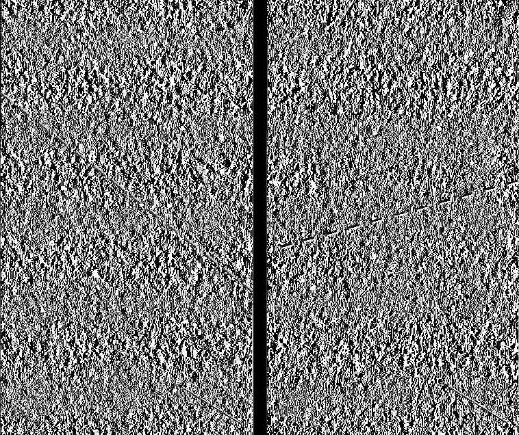
5 were taken while the platen and the wafer were both in rotation, and those presented here were picked from thousands of available images. The dark areas in the image correspond to low values of the ratio of intensities and indicate where the pad and the wafer are close to each other, or the tops of the pad asperities. Conversely, the lighter sections of the image indicate high values of the ratio and slurry filled valleys between pad asperities. Figure 2a is an image of the slurry layer between a Freudenberg FX9 polishing pad and a flat BK-7 wafer. Intimate contact of the pad and wafer would imply a boundary lubrication regime. Profilometer measurements of the Freudenberg FX9 pad indicate a surface roughness, R a = 4.3±0.3µm, suggesting that the asperity peak-to-valley height averages around 8.6µm. The image in figure 2a shows these peaks and valleys clearly, and one can estimate R a = 3.1±0.3 µm from roughly calibrating the images. This observation implies that the asperities are compressed 2-3 µm during polishing. In the future we plan to measure the percentage of the pad in contact with the wafer. Contact measurements require the absolute calibration mentioned earlier. In addition to detecting slurry flow over pad asperities, most images show patterns in the asperities as indicated by the dashed lines in figure 2. The striation lines in Figure 2a run from the top left to bottom right at almost 45 degrees. In figure 2b the striation lines are just off the horizontal with a slightly positive slope. These lines are most likely gouges in the pad caused by the diamond grit conditioner. Figure 2b shows a slurry layer beneath a 14.5µm deep, 1000µm square well etched into the BK7 wafer over a Freudenberg FX9 polishing pad. The overall average
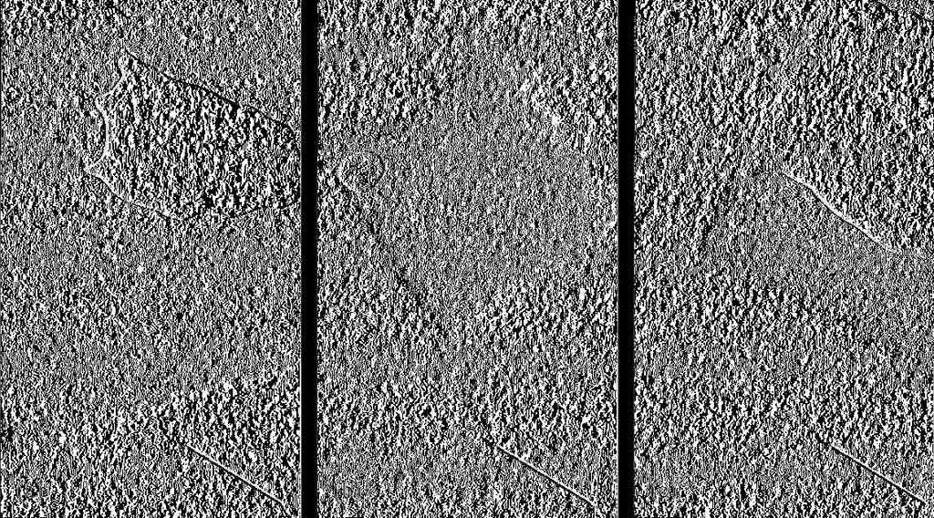
6 intensity underneath the square well is significantly higher than that of the surrounding region. These high intensity regions have no black areas indicating that the asperities are not in contact with the bottom of the well. Preliminary analysis of surface roughness based upon intensity measurements on this and similar images show that the average roughness beneath the contact regions is less than the roughness beneath the wells (difference of approximately 1µm). These data suggest asperity compression outside the well as in figure 2a, and the asperities have time to expand under the wells as both surfaces rotate. Figure 3 contains images from a polishing run with 27µm deep, square wells etched into a BK7 wafer over a Freudenberg FX9 pad. The arrows in figure 3 show the direction of slurry flow. The slurry does not always fill this deeper well completely leading to air pockets within the well. The majority of the images showed air bubbles of different sizes moving across the wells. Figure 3a shows an air pocket in the center of a well. The irregular shape can probably be attributed to slurry flowing around different size asperities. The majority of the images from the runs with a 27µm well are similar to figure 3b, showing air pockets in the upper left corner of the wells, which is the trailing edge of the slurry flow. Figure 3c shows one of the larger air pockets as it is dissipating through the contact region just behind the trailing edge of the well. The behavior of the air in these images implies that there is air entrapment, not cavitation, during the polishing process. One can also see the slurry in the pad below the air pocket, implying that one can estimate the dimensions and volume of the air bubble by comparing the fluorescence under the well outside of the air bubble as compared to inside the air bubble.
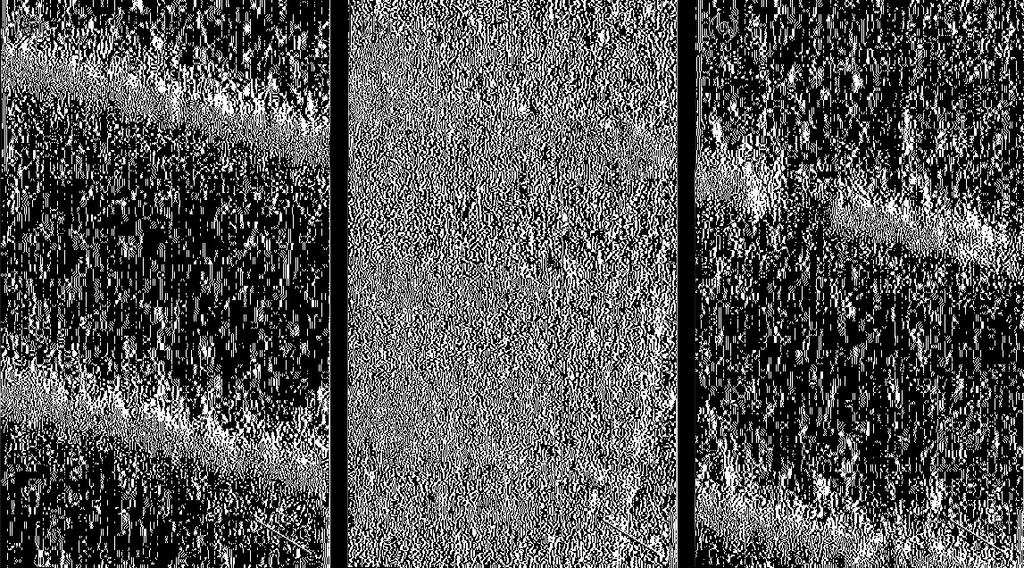
7 Figure 4 shows images of a BK7 wafer with 27µm wells over a Rodel IC1000 k- grooved pad. Figures 4a and 4b are the two extreme cases observed during this run where the grooves in the pad are completely filled (4a) and have almost no slurry present (4b). Most images indicated that the grooves were partially filled as in figure 4c. In these images, air pockets beneath the wells were confined to the grooves in the pad and did not accumulate at the trailing edge of the well as observed on the flat pad figure 3. Note that it is difficult to see the well in figure 4b because the amount of slurry in the groove is significantly greater than outside the groove. This same pad was used to observe the slurry layer beneath a wafer with 14 µm wells. The shallower wells were difficult to observe because the intensity contrast between the inside and outside of the wells was too low due to the dominance of the grooved regions. Figure 5 includes images from experimental polishing pads produced by Cabot Microelectronics Corporation. Figure 5a show the slurry layer between a flat BK7 wafer and the M2 thin grooved pad. Figure 5b shows fluid over an M3 xy-grooved pad. The M3 pad is slightly smoother than the M2 pad. Besides the obvious groove, the dominant features in image 5a are cross-hatched regions of high intensity indicating a pattern of valleys in the pad. This pattern was imprinted onto the pad with a woven material and tests the ability of the DELIF technique to observe larger scale features. It will not be present in the final version of this experimental pad. The surface roughness of these pads is an order of magnitude larger than the Fruedenberg FX-9 and Rodel IC1000 pads. Therefore, the intensity contrast between asperities in the Cabot pads overshadows even a
8 27µm deep well. These large asperities limit our ability to study pad rebound and surface roughness under a patterned wafer in a similar manner as discussed in figures 2 and 3. Conclusion Dual Emission Laser Induced Fluorescence (DELIF) has provided a means to directly observe the slurry layer thickness instantaneously during CMP for the first time at high spatial and temporal resolution. In-situ images are taken at a frequency of 2 Hz over an area of 1.6 x 2.7 mm with an exposure time of 20 ms. The fluid layers were observed between the wafer and several types of polishing pads that are commercially available and in development. Images were collected under both patterned and unpatterned wafers. A direct correlation between intensities in the ratio images and fluid film thickness can be done by comparing ratio values under patterned wells of two different depths, allowing the estimation of asperity compression during polishing. Deeper wells led to air pockets underneath wafer features and over both flat and grooved pads. Pad and wafer features can be distinguished using DELIF to observe the slurry layer provided that the features are of the same order of magnitude. Acknowledgements We would like to thank Intel and Cabot Microelectronics for the funding for this project. We are especially thankful for patterned and etched the BK7 wafers from Intel,
9 and for the experimental pads from Cabot Microelectronic. In addition, we thank Veeco Metrology for providing the profilometer and Freudenberg for providing pads. We also want to thank Mike Lacy from Cabot for helping take some of the images.
10 Figure Captions Figure 1. Experimental Setup. Slurry flow, conditioning, wafer and platen rotation are constant. The laser is directed through the wafer, excites the pad, which in turn excites the dye in the slurry. The two cameras observe the pad and the slurry fluorescence. Figure 2. The gray arrow indicates the slurry flow direction and the dashed white line indicates the conditioner striation direction. (a) The fluid layer during CMP of a flat wafer over a Freudenberg FX9 polishing pad. (b) Slurry film thickness between a wafer with etched 14.5µm deep square well over the Freudenberg FX9 pad. Figure 3. The fluid layer between a BK7 wafer with etched 27µm deep square wells and a Freudenberg FX9 polishing pad. Arrows denote slurry flow direction. (a) An irregularly shaped air pocket. (b) An air pocket at the trailing corner of the well. (c) An air pocket dissipating into the pad-wafer contact region. Figure 4. Slurry beneath a BK7 wafer with 27µm deep well on a Rodel IC100 k-grooved pad. Arrows denote slurry flow direction. (a) The grooves are completely filled with slurry. (b) The grooves have no slurry even under the square well. (c) Small air pockets are trapped in the grooves. Figure 5. Experimental polishing pads from Cabot Microelectronics. (a) The slurry layer between a flat BK7 wafer and an M2 thin grooved pad. (b) The slurry layer between a BK7 wafer with 27mm deep wells over an M3 x-y grooved pad.
11 References 1. L. Trotha, G. Mörsch, G. Zwicker, Semiconductor International, 27 (9), 54 (2004). 2. A. T. Kim, J. Seok, J. A. Tichy, T. S. Cale, Journal of the Electrochemical Society, 150 (9), G570 (2003). 3. Y. R. Jeng, H. J. Tsai. Journal of the Electrochemical Society, 150 (6), G348 (2003). 4. J. L. Yuan, B. Lin, Z. W. Shen, J. J. Zheng, J. Ruan, L. B. Zhang, Advances in Abrasive Processes Key Engineering Materials, 202, 85, (2001). 5. D. G. Thakurta, C. L. Borst, D. W. Schwendeman, R. J. Gutmann, W. N. Gill, Thin Solid Films, 366 (1-2), 181, (2000). 6. H. Liang, F. Kaufman, R. Sevilla, S. Anjur, Wear, 211 (2), 271, (1997). 7. B. Mullany, G. Byrne. Journal of Materials Processing Technology, 132, 28, (2003). 8. J. Lu, C. Rogers, V. P. Manno, A. Philipossian, S. Anjur, M. Moinpour, Journal of the Electrochemical Society, 151 (4), G241, (2004). 9. E. Chan, Instantaneous Mapping in Chemical Mechanical Planarization, Master s Thesis, Tufts University, (2003). 10. J. Copetta, C. Rogers, Experiments in Fluids, 25, 1, (1998). 11. C. H. Hidrovo, D. P. Hart, Measurement Science and Technology, 12, 467, (2001)
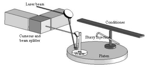
12 Figure 1
13
14
15
16
The Effect of Wafer Shape on Slurry Film Thickness and Friction Coefficients in Chemical Mechanical Planarization
 The Effect of Wafer Shape on Slurry Film Thickness and Friction Coefficients in Chemical Mechanical Planarization Joseph Lu a, Jonathan Coppeta a, Chris Rogers a, Vincent P. Manno a, Livia Racz a, Ara
Pad effects on slurry transport beneath a wafer during polishing
 Pad effects on slurry transport beneath a wafer during polishing Coppeta α, J., Racz χ, L., Philipossian δ,a., Kaufman ε, F., Rogers β, C., Affiliations: α= Research assistant, Tufts University, Department
Fundamental Characterizations of Diamond Disc, Pad, and Retaining Ring Wear in Chemical Mechanical Planarization Processes
 Fundamental Characterizations of Diamond Disc, Pad, and Retaining Ring Wear in Chemical Mechanical Planarization Processes Yun Zhuang 1,2, Len Borucki 1, Ara Philipossian 1,2 1. Araca, Inc., Tucson, Arizona
Improving the Collection Efficiency of Raman Scattering
 PERFORMANCE Unparalleled signal-to-noise ratio with diffraction-limited spectral and imaging resolution Deep-cooled CCD with excelon sensor technology Aberration-free optical design for uniform high resolution
Bias errors in PIV: the pixel locking effect revisited.
 Bias errors in PIV: the pixel locking effect revisited. E.F.J. Overmars 1, N.G.W. Warncke, C. Poelma and J. Westerweel 1: Laboratory for Aero & Hydrodynamics, University of Technology, Delft, The Netherlands,
Lithography. 3 rd. lecture: introduction. Prof. Yosi Shacham-Diamand. Fall 2004
 Lithography 3 rd lecture: introduction Prof. Yosi Shacham-Diamand Fall 2004 1 List of content Fundamental principles Characteristics parameters Exposure systems 2 Fundamental principles Aerial Image Exposure
Micromachined Shear Stress Sensors for Characterization of Surface Forces during Chemical Mechanical Polishing
 Mater. Res. Soc. Symp. Proc. Vol. 991 2007 Materials Research Society 0991-C06-03 Micromachined Shear Stress Sensors for Characterization of Surface Forces during Chemical Mechanical Polishing Andrew Mueller
Design, Characteristics and Performance of Diamond Pad Conditioners
 Reprinted from Mater. Res. Soc. Symp. Proc. Volume 1249 21 Materials Research Society 1249-E2-4 Design, Characteristics and Performance of Diamond Pad Conditioners Doug Pysher, Brian Goers, John Zabasajja
Development of Orderly Micro Asperity on Polishing Pad Surface for Chemical Mechanical Polishing (CMP) Process using Anisotropic Etching
 Process using Anisotropic Etching") AIJSTPME (2010) 3(3): 29-34 Development of Orderly Micro Asperity on Polishing Pad Surface for Chemical Mechanical Polishing (CMP) Process using Anisotropic Etching Khajornrungruang P., Kimura K. and Baba
AIJSTPME (2010) 3(3): 29-34 Development of Orderly Micro Asperity on Polishing Pad Surface for Chemical Mechanical Polishing (CMP) Process using Anisotropic Etching Khajornrungruang P., Kimura K. and Baba
Finishing first how automated systems improve the productivity and repeatability of wafer lapping and polishing
 Finishing first how automated systems improve the productivity and repeatability of wafer lapping and polishing Author: Mark Kennedy www.logitech.uk.com Overview The lapping and polishing of wafers for
Improved Cooling unit with Automatic Temperature Controller for Enhancing the Life of Ice Bonded Abrasive Polishing Tool
 Improved Cooling unit with Automatic Temperature Controller for Enhancing the Life of Ice Bonded Abrasive Polishing Tool S.Rambabu 1 and N. Ramesh Babu 2 * 1 Department of Mechanical Engineering, Indian
Parameter Optimization by Taguchi Methods for Polishing LiTaO3 Substrate. Using Force-induced Rheological Polishing Method
 ISAAT2018 Parameter Optimization by Taguchi Methods for Polishing LiTaO3 Substrate Using Force-induced Rheological Polishing Method Shihao Chen 1,a, Binghai Lv 1, b*,julong Yuan 1,c, Ping Zhao 1,d, Qi
Photolithography Technology and Application
 Photolithography Technology and Application Jeff Tsai Director, Graduate Institute of Electro-Optical Engineering Tatung University Art or Science? Lind width = 100 to 5 micron meter!! Resolution = ~ 3
No soft touch only automated systems can boost productivity and quality when lapping/polishing fragile GaAs wafers
 No soft touch only automated systems can boost productivity and quality when lapping/polishing fragile GaAs wafers Author: Mark Kennedy www.logitech.uk.com Overview The processing of GaAs (gallium arsenide)
LASER GENERATION AND DETECTION OF SURFACE ACOUSTIC WAVES
 LASER GENERATION AND DETECTION OF SURFACE ACOUSTIC WAVES USING GAS-COUPLED LASER ACOUSTIC DETECTION INTRODUCTION Yuqiao Yang, James N. Caron, and James B. Mehl Department of Physics and Astronomy University
EUV Substrate and Blank Inspection
 EUV Substrate and Blank Inspection SEMATECH EUV Workshop 10/11/99 Steve Biellak KLA-Tencor RAPID Division *This work is partially funded by NIST-ATP project 98-06, Project Manager Purabi Mazumdar 1 EUV
Vertical External Cavity Surface Emitting Laser
 Chapter 4 Optical-pumped Vertical External Cavity Surface Emitting Laser The booming laser techniques named VECSEL combine the flexibility of semiconductor band structure and advantages of solid-state
Feature-level Compensation & Control
 Feature-level Compensation & Control 2 Sensors and Control Nathan Cheung, Kameshwar Poolla, Costas Spanos Workshop 11/19/2003 3 Metrology, Control, and Integration Nathan Cheung, UCB SOI Wafers Multi wavelength
End-of-Chapter Exercises
 End-of-Chapter Exercises Exercises 1 12 are conceptual questions designed to see whether you understand the main concepts in the chapter. 1. Red laser light shines on a double slit, creating a pattern
Polishing Pad and Conditioning Disc Characterization and Wear Mechanisms
 Polishing Pad and Conditioning Disc Characterization and Wear Mechanisms Mater. Res. Soc. Symp. Proc. Vol. 991 2007 Materials Research Society 0991-C01-01 CMP Active Diamond Characterization and Conditioner
nanovea.com PROFILOMETERS 3D Non Contact Metrology
 PROFILOMETERS 3D Non Contact Metrology nanovea.com PROFILOMETER INTRO Nanovea 3D Non-Contact Profilometers are designed with leading edge optical pens using superior white light axial chromatism. Nano
Section 2: Lithography. Jaeger Chapter 2. EE143 Ali Javey Slide 5-1
 Section 2: Lithography Jaeger Chapter 2 EE143 Ali Javey Slide 5-1 The lithographic process EE143 Ali Javey Slide 5-2 Photolithographic Process (a) (b) (c) (d) (e) (f) (g) Substrate covered with silicon
NON-TRADITIONAL MACHINING PROCESSES ULTRASONIC, ELECTRO-DISCHARGE MACHINING (EDM), ELECTRO-CHEMICAL MACHINING (ECM)
, ELECTRO-CHEMICAL MACHINING (ECM)") NON-TRADITIONAL MACHINING PROCESSES ULTRASONIC, ELECTRO-DISCHARGE MACHINING (EDM), ELECTRO-CHEMICAL MACHINING (ECM) A machining process is called non-traditional if its material removal mechanism is basically
NON-TRADITIONAL MACHINING PROCESSES ULTRASONIC, ELECTRO-DISCHARGE MACHINING (EDM), ELECTRO-CHEMICAL MACHINING (ECM) A machining process is called non-traditional if its material removal mechanism is basically
Sensors and Metrology - 2 Optical Microscopy and Overlay Measurements
 Sensors and Metrology - 2 Optical Microscopy and Overlay Measurements 1 Optical Metrology Optical Microscopy What is its place in IC production? What are the limitations and the hopes? The issue of Alignment
Lab 3: Low-Speed Delta Wing
 2009 Lab 3: Low-Speed Delta Wing Innovative Scientific Solutions Inc. 2766 Indian Ripple Road Dayton, OH 45440 (937)-429-4980 Lab 3: Low-Speed Delta Wing Introduction: A wind tunnel is an important tool
Single-photon excitation of morphology dependent resonance
 Single-photon excitation of morphology dependent resonance 3.1 Introduction The examination of morphology dependent resonance (MDR) has been of considerable importance to many fields in optical science.
LOS 1 LASER OPTICS SET
 LOS 1 LASER OPTICS SET Contents 1 Introduction 3 2 Light interference 5 2.1 Light interference on a thin glass plate 6 2.2 Michelson s interferometer 7 3 Light diffraction 13 3.1 Light diffraction on a
TECHVIEW. Impact of Diamond CMP Conditioning Disk Characteristics on Removal Rates of Polyurethane Polishing Pads. abrasive technology
 abrasive technology TECHVIEW Impact of Diamond CMP Conditioning Disk Characteristics on Removal Rates of Polyurethane Polishing Pads Mark Bubnick, Sohail Qamar, Thomas Namola, and Dave McClew Abrasive
2. Pulsed Acoustic Microscopy and Picosecond Ultrasonics
 1st International Symposium on Laser Ultrasonics: Science, Technology and Applications July 16-18 2008, Montreal, Canada Picosecond Ultrasonic Microscopy of Semiconductor Nanostructures Thomas J GRIMSLEY
Acoustic resolution. photoacoustic Doppler velocimetry. in blood-mimicking fluids. Supplementary Information
 Acoustic resolution photoacoustic Doppler velocimetry in blood-mimicking fluids Joanna Brunker 1, *, Paul Beard 1 Supplementary Information 1 Department of Medical Physics and Biomedical Engineering, University
Photolithography I ( Part 1 )
") 1 Photolithography I ( Part 1 ) Chapter 13 : Semiconductor Manufacturing Technology by M. Quirk & J. Serda Bjørn-Ove Fimland, Department of Electronics and Telecommunication, Norwegian University of Science
1 Photolithography I ( Part 1 ) Chapter 13 : Semiconductor Manufacturing Technology by M. Quirk & J. Serda Bjørn-Ove Fimland, Department of Electronics and Telecommunication, Norwegian University of Science
Drilling of Glass by Excimer Laser Mask Projection Technique Abstract Introduction Experimental details
 Drilling of Glass by Excimer Laser Mask Projection Technique Bernd Keiper, Horst Exner, Udo Löschner, Thomas Kuntze Laserinstitut Mittelsachsen e.v., Hochschule Mittweida, University of Applied Sciences
Astigmatism Particle Tracking Velocimetry for Macroscopic Flows
 1TH INTERNATIONAL SMPOSIUM ON PARTICLE IMAGE VELOCIMETR - PIV13 Delft, The Netherlands, July 1-3, 213 Astigmatism Particle Tracking Velocimetry for Macroscopic Flows Thomas Fuchs, Rainer Hain and Christian
Section 2: Lithography. Jaeger Chapter 2 Litho Reader. The lithographic process
 Section 2: Lithography Jaeger Chapter 2 Litho Reader The lithographic process Photolithographic Process (a) (b) (c) (d) (e) (f) (g) Substrate covered with silicon dioxide barrier layer Positive photoresist
Akinori Mitani and Geoff Weiner BGGN 266 Spring 2013 Non-linear optics final report. Introduction and Background
 Akinori Mitani and Geoff Weiner BGGN 266 Spring 2013 Non-linear optics final report Introduction and Background Two-photon microscopy is a type of fluorescence microscopy using two-photon excitation. It
Die Prep Considerations for IC Device Applications CORWIL Technology 1635 McCarthy Blvd Milpitas, CA 95035
 Die Prep Considerations for IC Device Applications CORWIL Technology 1635 McCarthy Blvd Milpitas, CA 95035 Jonny Corrao Die Prep While quality, functional parts are the end goal for all semiconductor companies,
Characterization Microscope Nikon LV150
 Characterization Microscope Nikon LV150 Figure 1: Microscope Nikon LV150 Introduction This upright optical microscope is designed for investigating up to 150 mm (6 inch) semiconductor wafers but can also
Horiba LabRAM ARAMIS Raman Spectrometer Revision /28/2016 Page 1 of 11. Horiba Jobin-Yvon LabRAM Aramis - Raman Spectrometer
 Page 1 of 11 Horiba Jobin-Yvon LabRAM Aramis - Raman Spectrometer The Aramis Raman system is a software selectable multi-wavelength Raman system with mapping capabilities with a 400mm monochromator and
Section 2: Lithography. Jaeger Chapter 2 Litho Reader. EE143 Ali Javey Slide 5-1
 Section 2: Lithography Jaeger Chapter 2 Litho Reader EE143 Ali Javey Slide 5-1 The lithographic process EE143 Ali Javey Slide 5-2 Photolithographic Process (a) (b) (c) (d) (e) (f) (g) Substrate covered
Overlay accuracy a metal layer study
 Overlay accuracy a metal layer study Andrew Habermas 1, Brad Ferguson 1, Joel Seligson 2, Elyakim Kassel 2, Pavel Izikson 2 1 Cypress Semiconductor, 2401 East 86 th St, Bloomington, MN 55425, USA 2 KLA-Tencor,
Nanonics Systems are the Only SPMs that Allow for On-line Integration with Standard MicroRaman Geometries
 Nanonics Systems are the Only SPMs that Allow for On-line Integration with Standard MicroRaman Geometries 2002 Photonics Circle of Excellence Award PLC Ltd, England, a premier provider of Raman microspectral
USING PIV ON THE SPLASH WATER IN A PELTON TURBINE
 USING PIV ON THE SPLASH WATER IN A PELTON TURBINE B.List, J.Prost, H.-B. Matthias Institute for Waterpower and Pumps Vienna University of Technology 1040 Wien, Austria Abstract: At the Institute for Waterpower
Thermography. White Paper: Understanding Infrared Camera Thermal Image Quality
 Electrophysics Resource Center: White Paper: Understanding Infrared Camera 373E Route 46, Fairfield, NJ 07004 Phone: 973-882-0211 Fax: 973-882-0997 www.electrophysics.com Understanding Infared Camera Electrophysics
SUPPLEMENTARY INFORMATION
 Optically reconfigurable metasurfaces and photonic devices based on phase change materials S1: Schematic diagram of the experimental setup. A Ti-Sapphire femtosecond laser (Coherent Chameleon Vision S)
THEIMER - lamps. The optimal type for every application. Ga - Fe doped: Multi spectrum type TH...2 Ga - Pb doped: Dual spectrum type THS...
 The optimal type for every application 12 12 1 1 8 8 6 6 4 4 2 2 3 35 4 45 5 55 6 65 7 Xenon puls: For reprographic camera type KX... 3 32 34 36 38 4 42 44 46 48 5 52 54 56 58 6 Hg undoped: For UV curing
Noise Analysis of AHR Spectrometer Author: Andrew Xiang
 1. Introduction Noise Analysis of AHR Spectrometer Author: Andrew Xiang The noise from Spectrometer can be very confusing. We will categorize different noise and analyze them in this document from spectrometer
Quantum-Well Semiconductor Saturable Absorber Mirror
 Chapter 3 Quantum-Well Semiconductor Saturable Absorber Mirror The shallow modulation depth of quantum-dot saturable absorber is unfavorable to increasing pulse energy and peak power of Q-switched laser.
Nikon. King s College London. Imaging Centre. N-SIM guide NIKON IMAGING KING S COLLEGE LONDON
 N-SIM guide NIKON IMAGING CENTRE @ KING S COLLEGE LONDON Starting-up / Shut-down The NSIM hardware is calibrated after system warm-up occurs. It is recommended that you turn-on the system for at least
Part 5-1: Lithography
 Part 5-1: Lithography Yao-Joe Yang 1 Pattern Transfer (Patterning) Types of lithography systems: Optical X-ray electron beam writer (non-traditional, no masks) Two-dimensional pattern transfer: limited
880 Quantum Electronics Optional Lab Construct A Pulsed Dye Laser
 880 Quantum Electronics Optional Lab Construct A Pulsed Dye Laser The goal of this lab is to give you experience aligning a laser and getting it to lase more-or-less from scratch. There is no write-up
Applications of Steady-state Multichannel Spectroscopy in the Visible and NIR Spectral Region
 Feature Article JY Division I nformation Optical Spectroscopy Applications of Steady-state Multichannel Spectroscopy in the Visible and NIR Spectral Region Raymond Pini, Salvatore Atzeni Abstract Multichannel
Measurement of Surface Profile and Layer Cross-section with Wide Field of View and High Precision
 Hitachi Review Vol. 65 (2016), No. 7 243 Featured Articles Measurement of Surface Profile and Layer Cross-section with Wide Field of View and High Precision VS1000 Series Coherence Scanning Interferometer
Growing a NASA Sponsored Metrology Project to Serve Many Applications and Industries. James Millerd President, 4D Technology
 Growing a NASA Sponsored Metrology Project to Serve Many Applications and Industries James Millerd President, 4D Technology Outline In the Beginning Early Technology The NASA Connection NASA Programs First
CCD Analogy BUCKETS (PIXELS) HORIZONTAL CONVEYOR BELT (SERIAL REGISTER) VERTICAL CONVEYOR BELTS (CCD COLUMNS) RAIN (PHOTONS)
 HORIZONTAL CONVEYOR BELT (SERIAL REGISTER) VERTICAL CONVEYOR BELTS (CCD COLUMNS) RAIN (PHOTONS)") CCD Analogy RAIN (PHOTONS) VERTICAL CONVEYOR BELTS (CCD COLUMNS) BUCKETS (PIXELS) HORIZONTAL CONVEYOR BELT (SERIAL REGISTER) MEASURING CYLINDER (OUTPUT AMPLIFIER) Exposure finished, buckets now contain
CCD Analogy RAIN (PHOTONS) VERTICAL CONVEYOR BELTS (CCD COLUMNS) BUCKETS (PIXELS) HORIZONTAL CONVEYOR BELT (SERIAL REGISTER) MEASURING CYLINDER (OUTPUT AMPLIFIER) Exposure finished, buckets now contain
University of Wisconsin Chemistry 524 Spectroscopic Components *
 University of Wisconsin Chemistry 524 Spectroscopic Components * In journal articles, presentations, and textbooks, chemical instruments are often represented as block diagrams. These block diagrams highlight
CMP for More Than Moore
 2009 Levitronix Conference on CMP Gerfried Zwicker Fraunhofer Institute for Silicon Technology ISIT Itzehoe, Germany gerfried.zwicker@isit.fraunhofer.de Contents Moore s Law and More Than Moore Comparison:
The spectral colours of nanometers
 Reprint from the journal Mikroproduktion 3/2005 Berthold Michelt and Jochen Schulze The spectral colours of nanometers Precitec Optronik GmbH Raiffeisenstraße 5 D-63110 Rodgau Phone: +49 (0) 6106 8290-14
Understanding Infrared Camera Thermal Image Quality
 Access to the world s leading infrared imaging technology Noise { Clean Signal www.sofradir-ec.com Understanding Infared Camera Infrared Inspection White Paper Abstract You ve no doubt purchased a digital
Figure 1: A detailed sketch of the experimental set up.
 Electronic Supplementary Material (ESI) for Soft Matter. This journal is The Royal Society of Chemistry 2015 Supplementary Information Detailed Experimental Set Up camera 2 long range objective aluminum
PERFORMANCE OF PHOTODIGM S DBR SEMICONDUCTOR LASERS FOR PICOSECOND AND NANOSECOND PULSING APPLICATIONS
 PERFORMANCE OF PHOTODIGM S DBR SEMICONDUCTOR LASERS FOR PICOSECOND AND NANOSECOND PULSING APPLICATIONS By Jason O Daniel, Ph.D. TABLE OF CONTENTS 1. Introduction...1 2. Pulse Measurements for Pulse Widths
CAMAG TLC VISUALIZER 2
 CAMAG TLC VISUALIZER 2 Professional Imaging and Documentation System for TLC/HPTLC Chromatograms with a new Digital CCD Camera, connected by USB 3.0 WORLD LEADER IN PLANAR CHROMATOGRAPHY Visualization,
plasmonic nanoblock pair
 Nanostructured potential of optical trapping using a plasmonic nanoblock pair Yoshito Tanaka, Shogo Kaneda and Keiji Sasaki* Research Institute for Electronic Science, Hokkaido University, Sapporo 1-2,
REAL TIME SURFACE DEFORMATIONS MONITORING DURING LASER PROCESSING
 The 8 th International Conference of the Slovenian Society for Non-Destructive Testing»Application of Contemporary Non-Destructive Testing in Engineering«September 1-3, 2005, Portorož, Slovenia, pp. 335-339
KNIFE-EDGE RIGHT-ANGLE PRISM MIRRORS
 KNIFE-EDGE RIGHT-ANGLE PRISM MIRRORS Precision Cut Prisms Feature Bevel-Free 90 Angle Dielectric, Silver, Gold, and Aluminum Coatings Available 25 mm x 25 mm Faces Application Idea MRAK25-M01 Mounted on
Instructions for the Experiment
 Instructions for the Experiment Excitonic States in Atomically Thin Semiconductors 1. Introduction Alongside with electrical measurements, optical measurements are an indispensable tool for the study of
The End of Thresholds: Subwavelength Optical Linewidth Measurement Using the Flux-Area Technique
 The End of Thresholds: Subwavelength Optical Linewidth Measurement Using the Flux-Area Technique Peter Fiekowsky Automated Visual Inspection, Los Altos, California ABSTRACT The patented Flux-Area technique
CHAPTER 7. Waveguide writing in optimal conditions. 7.1 Introduction
 CHAPTER 7 7.1 Introduction In this chapter, we want to emphasize the technological interest of controlled laser-processing in dielectric materials. Since the first report of femtosecond laser induced refractive
Improved Radiometry for LED Arrays
 RadTech Europe 2017 Prague, Czech Republic Oct. 18, 2017 Improved Radiometry for LED Arrays Dr. Robin E. Wright 3M Corporate Research Process Laboratory, retired 3M 2017 All Rights Reserved. 1 Personal
ScanArray Overview. Principle of Operation. Instrument Components
 ScanArray Overview The GSI Lumonics ScanArrayÒ Microarray Analysis System is a scanning laser confocal fluorescence microscope that is used to determine the fluorescence intensity of a two-dimensional
Signal Analysis of CMP Process based on AE Monitoring System
 INTERNATIONAL JOURNAL OF PRECISION ENGINEERING AND MANUFACTURING-GREEN TECHNOLOGY Vol. 2, No. 1, pp. 15-19 JANUARY 2015 / 15 10.1007/s40684-015-0002-2 Signal Analysis of CMP Process based on AE Monitoring
Home Lab 13 Interference
 Home Lab Lab 13 Interference Home Lab 13 Interference Activity 13 1: Thin film interference of reflected light from air and glass interfaces Objective: To observe and describe interference phenomena Materials
Total Absorption Dual Readout Calorimetry R&D
 Available online at www.sciencedirect.com Physics Procedia 37 (2012 ) 309 316 TIPP 2011 - Technology and Instrumentation for Particle Physics 2011 Total Absorption Dual Readout Calorimetry R&D B. Bilki
SUPPLEMENTARY INFORMATION
 Room-temperature continuous-wave electrically injected InGaN-based laser directly grown on Si Authors: Yi Sun 1,2, Kun Zhou 1, Qian Sun 1 *, Jianping Liu 1, Meixin Feng 1, Zengcheng Li 1, Yu Zhou 1, Liqun
CHARACTERIZATION AND FIRST APPLICATION OF A THIN-FILM ELECTRET UNSTEADY PRESSURE MEASUREMENT TECHNIQUE
 XIX Biannual Symposium on Measuring Techniques in Turbomachinery Transonic and Supersonic Flow in CHARACTERIZATION AND FIRST APPLICATION OF A THIN-FILM ELECTRET UNSTEADY PRESSURE MEASUREMENT TECHNIQUE
Chapter 17: Wave Optics. What is Light? The Models of Light 1/11/13
 Chapter 17: Wave Optics Key Terms Wave model Ray model Diffraction Refraction Fringe spacing Diffraction grating Thin-film interference What is Light? Light is the chameleon of the physical world. Under
Bandpass Edge Dichroic Notch & More
 Edmund Optics BROCHURE Filters COPYRIGHT 217 EDMUND OPTICS, INC. ALL RIGHTS RESERVED 1/17 Bandpass Edge Dichroic Notch & More Contact us for a Stock or Custom Quote Today! USA: +1-856-547-3488 EUROPE:
APRAD SOR Excimer group -Progress Report 2011-
 APRAD SOR Excimer group -Progress Report 011- The DPP EUV source activity During 011 the work on the DPP (Discharge Produced Plasma) source of Extreme Ultraviolet (EUV) radiation has been devoted to a
Defense Technical Information Center Compilation Part Notice
 UNCLASSIFIED Defense Technical Information Center Compilation Part Notice ADPO 11345 TITLE: Measurement of the Spatial Frequency Response [SFR] of Digital Still-Picture Cameras Using a Modified Slanted
An Introduction to CCDs. The basic principles of CCD Imaging is explained.
 An Introduction to CCDs. The basic principles of CCD Imaging is explained. Morning Brain Teaser What is a CCD? Charge Coupled Devices (CCDs), invented in the 1970s as memory devices. They improved the
Nano-structured superconducting single-photon detector
 Nano-structured superconducting single-photon detector G. Gol'tsman *a, A. Korneev a,v. Izbenko a, K. Smirnov a, P. Kouminov a, B. Voronov a, A. Verevkin b, J. Zhang b, A. Pearlman b, W. Slysz b, and R.
Lecture 7. Lithography and Pattern Transfer. Reading: Chapter 7
 Lecture 7 Lithography and Pattern Transfer Reading: Chapter 7 Used for Pattern transfer into oxides, metals, semiconductors. 3 types of Photoresists (PR): Lithography and Photoresists 1.) Positive: PR
Title: Laser marking with graded contrast micro crack inside transparent material using UV ns pulse
 Cover Page Title: Laser marking with graded contrast micro crack inside transparent material using UV ns pulse laser Authors: Futoshi MATSUI*(1,2), Masaaki ASHIHARA(1), Mitsuyasu MATSUO (1), Sakae KAWATO(2),
Scintillation Counters
 PHY311/312 Detectors for Nuclear and Particle Physics Dr. C.N. Booth Scintillation Counters Unlike many other particle detectors, which exploit the ionisation produced by the passage of a charged particle,
3D light microscopy techniques
 3D light microscopy techniques The image of a point is a 3D feature In-focus image Out-of-focus image The image of a point is not a point Point Spread Function (PSF) 1D imaging 2D imaging 3D imaging Resolution
SUPPLEMENTARY INFORMATION
 Transfer printing stacked nanomembrane lasers on silicon Hongjun Yang 1,3, Deyin Zhao 1, Santhad Chuwongin 1, Jung-Hun Seo 2, Weiquan Yang 1, Yichen Shuai 1, Jesper Berggren 4, Mattias Hammar 4, Zhenqiang
Laser Scanning for Surface Analysis of Transparent Samples - An Experimental Feasibility Study
 STR/03/044/PM Laser Scanning for Surface Analysis of Transparent Samples - An Experimental Feasibility Study E. Lea Abstract An experimental investigation of a surface analysis method has been carried
Study of Hydrocarbon Detection Methods in Offshore Deepwater Sediments, Gulf of Guinea*
 Study of Hydrocarbon Detection Methods in Offshore Deepwater Sediments, Gulf of Guinea* Guoping Zuo 1, Fuliang Lu 1, Guozhang Fan 1, and Dali Shao 1 Search and Discovery Article #40999 (2012)** Posted
Silicon wafer thickness monitor
 Silicon wafer thickness monitor SIT-200 Alnair Labs Corporation 2016.04.20 Principle of Measurement Silicon wafer Optical fiber Sensor head Wavelength tunable laser PD PD Interference signal Power monitor
Evaluation of laser-based active thermography for the inspection of optoelectronic devices
 More info about this article: http://www.ndt.net/?id=15849 Evaluation of laser-based active thermography for the inspection of optoelectronic devices by E. Kollorz, M. Boehnel, S. Mohr, W. Holub, U. Hassler
Measurement of Temperature, Soot Diameter and Soot Volume Fraction in a Gulder Burner
 Department of Engineering Science University of Oxford Measurement of Temperature, Soot Diameter and Soot Volume Fraction in a Gulder Burner Huayong Zhao, Ben William, Richard Stone Project Meeting in
Characterization of Surface Structures using THz Radar Techniques with Spatial Beam Filtering and Out-of-Focus Detection
 ECNDT 2006 - Tu.2.8.3 Characterization of Surface Structures using THz Radar Techniques with Spatial Beam Filtering and Out-of-Focus Detection Torsten LÖFFLER, Bernd HILS, Hartmut G. ROSKOS, Phys. Inst.
AP Physics Problems -- Waves and Light
 AP Physics Problems -- Waves and Light 1. 1974-3 (Geometric Optics) An object 1.0 cm high is placed 4 cm away from a converging lens having a focal length of 3 cm. a. Sketch a principal ray diagram for
Why and How? Daniel Gitler Dept. of Physiology Ben-Gurion University of the Negev. Microscopy course, Michmoret Dec 2005
 Why and How? Daniel Gitler Dept. of Physiology Ben-Gurion University of the Negev Why use confocal microscopy? Principles of the laser scanning confocal microscope. Image resolution. Manipulating the
Sunlight Readability and Durability of Projected Capacitive Touch Displays for Outdoor Applications
 Sunlight Readability and Durability of By: Mike Harris, Product Manager, Ocular Touch, LLC Sunlight Readability Projected capacitive (PCAP) touch panels are rapidly replacing traditional mechanical methods
The absorption of the light may be intrinsic or extrinsic
 Attenuation Fiber Attenuation Types 1- Material Absorption losses 2- Intrinsic Absorption 3- Extrinsic Absorption 4- Scattering losses (Linear and nonlinear) 5- Bending Losses (Micro & Macro) Material
Copyright 2000 Society of Photo Instrumentation Engineers.
 Copyright 2000 Society of Photo Instrumentation Engineers. This paper was published in SPIE Proceedings, Volume 4043 and is made available as an electronic reprint with permission of SPIE. One print or
Fast Raman Spectral Imaging Using Chirped Femtosecond Lasers
 Fast Raman Spectral Imaging Using Chirped Femtosecond Lasers Dan Fu 1, Gary Holtom 1, Christian Freudiger 1, Xu Zhang 2, Xiaoliang Sunney Xie 1 1. Department of Chemistry and Chemical Biology, Harvard
Lecture 18: Photodetectors
 Lecture 18: Photodetectors Contents 1 Introduction 1 2 Photodetector principle 2 3 Photoconductor 4 4 Photodiodes 6 4.1 Heterojunction photodiode.................... 8 4.2 Metal-semiconductor photodiode................
Unit Test Strand: The Wave Nature of Light
 22K 11T 2A 3C Unit Test Strand: The Wave Nature of Light Expectations: E1. analyse technologies that use the wave nature of light, and assess their impact on society and the environment; E2. investigate,
Advances in Laser Micro-machining for Wafer Probing and Trimming
 Advances in Laser Micro-machining for Wafer Probing and Trimming M.R.H. Knowles, A.I.Bell, G. Rutterford & A. Webb Oxford Lasers June 10, 2002 Oxford Lasers June 2002 1 Introduction to Laser Micro-machining