High Spectral Resolution Plasmonic Color Filters with Subwavelength Dimensions Supplemental Information
|
|
|
- Elizabeth Lambert
- 5 years ago
- Views:
Transcription
1 High Spectral Resolution Plasmonic Color Filters with Subwavelength Dimensions Supplemental Information Dagny Fleischman 1, Katherine T. Fountaine 2, Colton R. Bukowsky 1, Giulia Tagliabue 1, Luke A. Sweatlock 2, and Harry A. Atwater 1 1. Thomas J. Watson Laboratories of Applied Physics, California Institute of Technology, Pasadena, CA Northrop Grumman NG Next, One Space Park, Redondo Beach, CA 90250, USA 16 pages, 8 figures, no tables Contents: 1. Transmission Response. 2. Optimization Method. 3. Fabrication Method. 4. Measurement Set-up and Analysis.
2 S1 Transmission Response The single narrowband transmission peak of the optimized filter arises from the coupling of a large number of modes within the mirrored filter structure. The blue transmission curves in Supplemental Figure S1(a)-(c) is the champion filter identified by the numerical optimization method. The red, green, and violet curves are all deviations from the ideal geometry that illuminate the connection between the physical parameters and the optical response. The suppressed transmission in the red curve in Supplemental Figure S1(a) is due to a weak gap mode that prevents the modes supported by this filter from outcoupling into the far-field (a representative mode supported by this structure is shown in Supplemental Figure S2(b)). This gap mode, shown in Supplmental Figure S2(a) has a weaker electric field intensity than those of the two filters with higher transmission efficiency shown in Supplemental Figures S2 (c) and (g) (the green and violet curves in Supplemental Figure S1(b) and (c). The primary source of the narrowband transmission is the thickness of the metal film spanning the region between the two mirrors. In Supplemental Figure S1(b), the physical parameters of the green curve filter are identical to that of the blue filter except that the green filter s film is twice the thickness of the blue filter. Increasing the thickness of the film pushes it outside the range of the skin depth of visible light, thereby preventing SPP modes from coupling across the surface of the film. The mode profiles verify that the supported modes only couple across the film in the thin film case. There is no evidence of cross-film coupling in the supported modes of the green curve filter (shown in Supplemental Figure S2(d) and (e)), but the thin film case clearly possesses crossfilm coupling, as shown in Supplemental Figure S2(f). By combining these conditions, a supported gap mode and cross-film coupling, it is possible to produce narrowband transmission features. The filter shown in the violet curve in Supplemental Figure S1(c) possesses a thin film and multiple narrow transmission features. Each of these features correspond to different supported modes in the structure. An example of a supported mode was determined for the peak at 688 nm and is shown in Supplemental Figure S2(h) which illustrates a cavity mode coupled to SPPs on the surfaces of the mirrors. This mode penetrates the thin film, as shown by both the non-zero field in the film and the weak SPPs supported on the film outside the cavity. The efficient gap mode shown in Supplemental Figure S2(g) allows for this
3 S2 mode to out-couple for a transmission response. The dimensions for all filters described in Supplemental Figures S1 and S2 are listed in Supplemental Table S1. The mode profiles shown in Supplmental Figure S2 were all calculated using Lumerical s MODE solver for the four filters shown in Supplemental Figure S1. Optimization Method The process for optimizing the filter structure using the NOMAD algorithm and this FOM (main text, Eqn. 1) is illustrated in Supplemental Figure S3. All steps are performed automatically after the optimization process is initiated, using the optimization defaults unless indicated in Supplementary Table S2. In this method, the algorithm suggests a set of physical parameters for the filter. Lumerical Finite Difference Time Domain simulation package (FDTD), and eigenmode solver, then uses these parameters to perform a simulation to determine the filter s optical response. The resulting transmission spectrum of the filter is then analyzed by a custom peakfinding algorithm, which was developed to include both the maxima at the edges of a vector and plateaus, to make sure that all peak-like features would be properly identified and accounted for. Using the analyzed spectrum, the FOM is calculated, and used by NOMAD to suggest a new set of physical parameters. This process repeats until the convergence criteria is met. Fabrication Method The filters were fabricated using a novel metal imprinting process, shown in Supplemental Figure S4, which produces mirrors with straighter sidewalls than lift-off processing with the added benefit of producing extremely smooth metal structures. The initial steps shown in this process define SiO2 structures that form the negative space around the metal mirrors using electron beam lithography. The fused silica chips are first sonicated in acetone before being rinsed in IPA. Next, a single layer of 950 A4 PMMA is spun at 1500 rpm for 1 minute and then baked for 5 minutes at 180 C. The fused silica substrate is electrically insulating, so a 5 nm Al film is thermally deposited on top of the resist to reduce charging during electron-beam patterning step. Electron-beam lithography is then used to write squares and rectangles that will eventually be the SiO2 regions between the mirrors. After the patterning step, the Al film is etched away using 30% TMAH for 50 seconds, then the substrate is rinsed with DI water. The PMMA is then developed using MIBK:IPA 1:3 for 30 seconds and the substrate is rinsed in IPA.
4 S3 Next, a 60 nm Cr film is deposited via electron beam evaporation at 0.6A/s in a chamber at pressure 5.3x10⁻⁷ torr. The PMMA and unwanted Cr are then removed via lift off using Remover PG for 5 minutes and occasional sonication. The remaining Cr film is used as an etch mask during a 1:54 m:s ICP etch in C4F8/O2 that defines 600 nm tall SiO2 pillars. The Cr etch mask is then removed by a 20 minute soak in Cr-7S etchant solution. Once the Cr is removed, a 1 nm layer of HfO2 is deposited via an 8 cycle deposition in an ALD. Next, 2 μm of Ag is deposited on top of the sample. The sample is rotated to try to ensure as conformal a deposition as possible. The height of the SiO2 pillars prevents completely infilling of the regions between the pillars. To create Ag mirrors that are flush to the SiO2 pillars, a wafer bonder was used to press a dummy chip of thermal SiO2 on Si onto the Ag film. The stack is held at 1500 torr and 175 C overnight, to allow the Ag to infill into the voids near the SiO2 pillar and the top of the film to reach the smoothness of the SiO2 on Si dummy chip. This process also considerably reduces the surface roughness of metal films, decreasing the RMS roughness of the as-deposited film from 5.58 nm down to 0.55 nm, as shown by the AFM scans in Supplemental Figure S5. After the Ag is pressed around the SiO2 pillar to form the mirrors, there is a 1.48 μm thick film of Ag on top of the pillar that must be milled to the final 50 nm thickness. An Ar mill in an ICP plasma etch system was used to remove the excess Ag. Different grains in Ag etch at different rates, so the forward power was increased to its maximum value of 300W to make the etch as physical as possible. The sample was milled for 6 minutes at a rate of 205 nm/min yielding a 255 nm thick film. The etch was stopped before the final 50 nm was reached to do a second pressing step to smooth out any thickness variations due to the grain texturing. The Ag film is then etched for another 32 seconds to bring the final thickness to 50 nm. These 50 nm Ag films are relatively transparent to back scattered electrons generated by a 30 kv and 100 na electron beam. This transparency was used to align the slit between the mirrors during the FIB process. While a 30 kv Ga beam does not generate enough back scattered electrons for
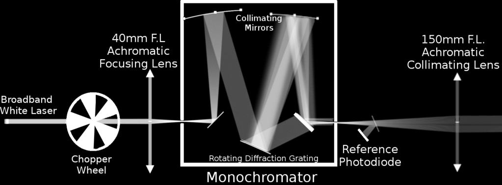
5 S4 visibility, by aligning the electron and ion beams to a coincident point, the proper position can be observed using the electron beam and then milled using a low current ion beam. Once the slits were milled, 1.4 μm of SiO2 were deposited in a PECVD using SiH4/Ar. The films deposited in the PECVD used are not conformal at the edges of chips, so to prevent the sample from oxidizing, an additional 8 nm of Al2O3 was deposited in an ALD on top of the SiO2 film to ensure the sample was completely encapsulated. To prevent the H2O precursor from oxidizing the edges during the ALD processing, the sample was first coated with extra-long pulses of the Al2O3 precursor and then subject to 40 cycles of 50 C Al2O3 depositions before depositing the final 4nm at 150 C 1. Cross-sections of a filter prior to milling and a completed filter are shown in Figure S4(a) and (b) of the main text. While the fabrication process used to make the measured filters uses serial patterning systems such as electron beam lithography, focused ion milling, and makes unconventional use of a wafer bonder, these filters can be fabricated in a nanofabrication foundry environment. The electron beam lithography and focused ion milling steps can also be replaced by a two-step aligned photolithography process that defines two SiO2 pillars. During the first photolithography step, a small pillar that will become the slit can be etched onto an SiO2 film. In the second photolithography process, a larger pillar can be defined under the small pillar to become the spacing between the mirrors. After the metal is deposited on the stacked pillars, a chemical mechanical polishing system can be used to thin the metal down and smooth it flat, leaving the top of the slit exposed, and finishing the filter with the final SiO2 coating step. Measurement Set-up and Analysis The custom-built optical transmission measurement set-ups used in this work are shown schematically in Supplemental Figure S6. In this configuration, a beam supplied by a NKT SuperK Extreme white laser was monochromated with variable slit width to give a constant bandpass of 2nm, collimated, expanded by two 90 degree off-axis parabolic mirrors, and finally focused onto the sample with a long working distance, low-na objective (Mitutoyo Plan Apo 50X,
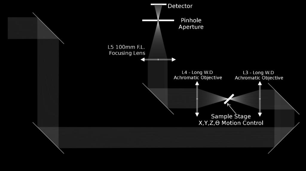
6 S5 Tube Length 200mm, NA=0.55). Using a CMOS (IDS UI-1460SE) camera we characterized experimentally the beam shape at the focal plane and verified it had a FWHM of ~2nm. A calibrated Si photodetector (Newport 818-ST2-UV) was used to measure the power transmitted through the filter, as well as the reference 5um aperture. During all measurements the beam was sampled with a glass slide and measured with a Si reference photodiode for simultaneous recording of the beam photocurrent, allowing correction of any fluctuations in the laser power between a normalization measurement and measurement of the samples. A chopper, typically at a frequency of 95Hz, was used to modulate the incident beam, and provide a reference frequency to two Stanford Research Systems SR840 lock-in amplifiers. An external, low-noise current-to-voltage transimpedance amplifier was used to feed both photodiode signals to the respective lock-in amplifier. The lock-in amplifiers were used to filter the modulated signal from other potential noise signals in the photodiode responses. In order to attenuate background signal as much as possible, the optical transmission setup described above was further modified into a transmission confocal microscopy configuration. The same monochromatic and collimated beam was redirected 180 via mirrors to enter the objective passing through its focal point. A second objective (Mitutoyo Plan Apo 2X, Tube Length 200mm, NA=0.05) focused and collimated the beam at the focal spot. The back side of the filter being measured was placed at the focal point of the high N.A. objective, creating a transfer function of the transmitted light. This collimated beam was refocused with a 100mm focal length planoconvex lens to form an image of the transmitted light. A 50μm pinhole was placed in this image plane. The portion of the image transmitted by the pinhole was controlled by translating the sample, rather than the pin-hole in the image plane. Due to the tube length being larger than 200mm, the actual magnification of this image was about 62x. The equivalent diameter of the aperture with respect to the magnified image was about 5μm as measured by the CMOS camera. A low dark current photodiode was used behind this pinhole to measure the transmitted photocurrent through the lock-in amplifier system. The imaging objective was calibrated for chromatic focal shifts and the position of the objective was adjusted with sub-micrometer steps to further reduce chromatic aberrations. Peak normalized signal-to-noise (SNR) plots were created using this method because it significantly increased spatial signal contrast and greatly reduced the background spectrum such that sub-percent peaks could be detected without a loss in SNR. The
7 S6 normalization spectrum for each filter was measured on an area of the fused silica superstrate where no Ag film existed, which accounted for the reflection of the superstrate. Angle Dependence of Mirrored Filters The transmitted peak position of the mirrored filters is independent of incident angle. As shown in Supplemental Figure S8, when an incident plane wave is injected at angles ranging from 0 to 40, the transmitted peak position does not shift. The transmission efficiency is reduced with increasing angle, because as the incident angle gets steeper, progressively more of the light is incident on the perfectly matched layer (PML) boundaries surrounding the simulation region instead of onto the filter itself, leading to an effective reduction of the apparent transmission. The angle insensitivity of the filters was further confirmed by simulating the transmission response of the filters when illuminated with Gaussian beams with varying numerical apertures (NAs). As the NA increased, the transmission efficiency also increased, because more of the incident light was focused into the region between the two mirrors in the filter. The angle insensitivity of these filters prevented any detrimental effects from the increased angular distribution of the incident light from the higher NA Gaussians.
8 S7 Figures Supplemental Figure S1: (a) comparison between a champion filter (blue) and a filter with reduced transmission (red). The red curve filter possesses a much smaller mirror spacing than the champion filter and a thicker film, which prevent efficient out-coupling of the supported modes (b) comparison between a champion filter (blue) and a filter (green) with the same physical parameters except for a thicker film, indicating that the thickness of the film between the mirrors plays a very large role in the narrow transmission bandwidth. (c) comparison between a chamption filter (blue) and a filter (violet) with multiple resonances that produce narrow transmission features. The physical parameters of all filters shown are listed in Supplementary Table S1. Representative mode profiles for each of these filters are shown in Supplemental Figure S2

9 S8
 prevents efficient outcoupling of the mode shown in (b), which leads to this filter s low transmission intensity.")
10 Supplemental Figure S2: (a) and (b) are electric field intensity mode profiles for Supplmental Figure S1(a) red curve filter calculated at 547 nm. The relatively weak gap mode in (a) prevents efficient outcoupling of the mode shown in (b), which leads to this filter s low transmission intensity. (c)-(e) are mode profiles for the green curve filter shown in Supplemental Figure S1(b) calculated at 614 nm. The more efficient gap mode allows for a higher out-coupling of the cavity mode shown in (d) and the SPP shown in (e), which is reflected in the transmission curve shown in Supplemental Figure S1(b). The transmission features are still relatively broad, but by reducing the thickness of the metal film, while holding the rest of the physical parameters of this fixed, the transmission peak can be narrowed. A mode profile calculated at the filter transmission peak at 554 nm is shown in (f) where it is possible to see electric field intensity spanning the thin film, indicating that the top and bottom surface SPPs are coupled and interacting, leading to a much reduced bandpass for this filter relative to the thick film case. (g) and (h) are the mode profiles calculated for the violet curve shown in Supplemental Figure S1(c) at 688 nm, which posseses multiple narrow transmission features. (g) indicates, as expected, that the gap mode is efficient enough to allow for modes to couple out of the filter. The profile shown in (h) indicates that the interacting cavity and SPP modes also couple to the SPPs on the far side of the thin film, which lead to the sharp transmission features present in this filters spectral response. S9
11 Supplemental Figure S3: The components of the filter optimization process. The Nonlinear Mesh Adaptive Direct Search algorithm (NOMAD) determines the parameters probed to find the optimal solution. Once the physical parameters (x) are selected, they will either be evaluated by the surrogate function or a Lumerical calculation, which return the FOM to NOMAD. For each Lumerical calculation, the transmission response is analyzed by the peak finding algorithm to determine the FOM, which can then be used by NOMAD S10

12 Supplemental Figure S4: The process flow for fabricating mirrored filters. First the region between the mirrors is defined in a fused silica substrate using a pattern defined by electron-beam lithography that is subsequently dry etched. Next a thick layer of Ag is deposited and pressed into the etched regions to form the mirrors. The Ag is then thinned to the final thickness of the thing film and the slit is milled before SiO2 is deposited on the top surface to encapsulate the Ag. S11
 An Ag film deposited in the same conditions that was then pressed at 1400 torr and held at 100 C for 6 hours that has an RMS of 0.")
13 Supplemental Figure S5: AFM scans illustrating the smoothing effect of the wafer bonder pressing process. (a) An electron beam evaporated Ag film that was not pressed. The RMS roughness is 5.58 nm (b) An Ag film deposited in the same conditions that was then pressed at 1400 torr and held at 100 C for 6 hours that has an RMS of 0.55 nm S12
 (c)")


14 S13 (a) (b) (c)
15 Supplemental Figure S6 (a) Schematic of the optical set-up depicting the monochromation and collimation of the light beam and the collection of the reference signal (b) Schematic of the focusing of light onto the sample and the collection of the transmitted signal with a Si Photodetector. (c) Schematic of the confocal transmission microscopy configuration. The ultracompact Ag filter transmits light into the high N.A. objective and it is imaged onto a pinhole aperture which selects a 5um diameter portion of the image signal. S14
16 Supplemental Figure S7: A sample simulated transmission response for a near IR mirrored color filter that has Cu metal components S15

17 Supplemental Figure S8: The angle dependence of a linear mirrored filter illuminated with a plane wave with angle of incidence ranging from 0 to 40 S17
18 S16 Tables Supplementary Table S1 Curve Blue Red Magenta Green Mirror Spacing Mirror Height Film Thickness Gap Width Oxide Thickness Supplementary Table S1: Physical parameters for the filters with responses plotted in Supplemental Figure S1. All dimensions are in nm. Supplementary Table S2 Setting Filter Optimization Default Surrogate Sample Points Minimum Mesh Size 1e-3 1e-4 Initial Mesh Size Surrogate Minimum Mesh Size Supplementary Table S2: Settings where the NOMAD defaults vary from those used during the Mirrored Filter Optimization References 1. Wood, J. D. et al. Effective passivation of exfoliated black phosphorus transistors against ambient degradation. Nano Lett. 14, (2014).
Supporting Information 1. Experimental
 Supporting Information 1. Experimental The position markers were fabricated by electron-beam lithography. To improve the nanoparticle distribution when depositing aqueous Ag nanoparticles onto the window,
Supplementary information for Stretchable photonic crystal cavity with
 Supplementary information for Stretchable photonic crystal cavity with wide frequency tunability Chun L. Yu, 1,, Hyunwoo Kim, 1, Nathalie de Leon, 1,2 Ian W. Frank, 3 Jacob T. Robinson, 1,! Murray McCutcheon,
plasmonic nanoblock pair
 Nanostructured potential of optical trapping using a plasmonic nanoblock pair Yoshito Tanaka, Shogo Kaneda and Keiji Sasaki* Research Institute for Electronic Science, Hokkaido University, Sapporo 1-2,
SUPPLEMENTARY INFORMATION
 Room-temperature continuous-wave electrically injected InGaN-based laser directly grown on Si Authors: Yi Sun 1,2, Kun Zhou 1, Qian Sun 1 *, Jianping Liu 1, Meixin Feng 1, Zengcheng Li 1, Yu Zhou 1, Liqun
Major Fabrication Steps in MOS Process Flow
 Major Fabrication Steps in MOS Process Flow UV light Mask oxygen Silicon dioxide photoresist exposed photoresist oxide Silicon substrate Oxidation (Field oxide) Photoresist Coating Mask-Wafer Alignment
Lithography. 3 rd. lecture: introduction. Prof. Yosi Shacham-Diamand. Fall 2004
 Lithography 3 rd lecture: introduction Prof. Yosi Shacham-Diamand Fall 2004 1 List of content Fundamental principles Characteristics parameters Exposure systems 2 Fundamental principles Aerial Image Exposure
SUPPLEMENTARY INFORMATION
 Transfer printing stacked nanomembrane lasers on silicon Hongjun Yang 1,3, Deyin Zhao 1, Santhad Chuwongin 1, Jung-Hun Seo 2, Weiquan Yang 1, Yichen Shuai 1, Jesper Berggren 4, Mattias Hammar 4, Zhenqiang
Monolithically integrated InGaAs nanowires on 3D. structured silicon-on-insulator as a new platform for. full optical links
 Monolithically integrated InGaAs nanowires on 3D structured silicon-on-insulator as a new platform for full optical links Hyunseok Kim 1, Alan C. Farrell 1, Pradeep Senanayake 1, Wook-Jae Lee 1,* & Diana.
Tunable Color Filters Based on Metal-Insulator-Metal Resonators
 Chapter 6 Tunable Color Filters Based on Metal-Insulator-Metal Resonators 6.1 Introduction In this chapter, we discuss the culmination of Chapters 3, 4, and 5. We report a method for filtering white light
A process for, and optical performance of, a low cost Wire Grid Polarizer
 1.0 Introduction A process for, and optical performance of, a low cost Wire Grid Polarizer M.P.C.Watts, M. Little, E. Egan, A. Hochbaum, Chad Jones, S. Stephansen Agoura Technology Low angle shadowed deposition
photolithographic techniques (1). Molybdenum electrodes (50 nm thick) are deposited by
. Molybdenum electrodes (50 nm thick) are deposited by") Supporting online material Materials and Methods Single-walled carbon nanotube (SWNT) devices are fabricated using standard photolithographic techniques (1). Molybdenum electrodes (50 nm thick) are deposited
Supporting online material Materials and Methods Single-walled carbon nanotube (SWNT) devices are fabricated using standard photolithographic techniques (1). Molybdenum electrodes (50 nm thick) are deposited
Bandpass Edge Dichroic Notch & More
 Edmund Optics BROCHURE Filters COPYRIGHT 217 EDMUND OPTICS, INC. ALL RIGHTS RESERVED 1/17 Bandpass Edge Dichroic Notch & More Contact us for a Stock or Custom Quote Today! USA: +1-856-547-3488 EUROPE:
Characteristics of point-focus Simultaneous Spatial and temporal Focusing (SSTF) as a two-photon excited fluorescence microscopy
 as a two-photon excited fluorescence microscopy") Characteristics of point-focus Simultaneous Spatial and temporal Focusing (SSTF) as a two-photon excited fluorescence microscopy Qiyuan Song (M2) and Aoi Nakamura (B4) Abstracts: We theoretically and experimentally
Characteristics of point-focus Simultaneous Spatial and temporal Focusing (SSTF) as a two-photon excited fluorescence microscopy Qiyuan Song (M2) and Aoi Nakamura (B4) Abstracts: We theoretically and experimentally
5. Lithography. 1. photolithography intro: overall, clean room 2. principle 3. tools 4. pattern transfer 5. resolution 6. next-gen
 5. Lithography 1. photolithography intro: overall, clean room 2. principle 3. tools 4. pattern transfer 5. resolution 6. next-gen References: Semiconductor Devices: Physics and Technology. 2 nd Ed. SM
Confocal Imaging Through Scattering Media with a Volume Holographic Filter
 Confocal Imaging Through Scattering Media with a Volume Holographic Filter Michal Balberg +, George Barbastathis*, Sergio Fantini % and David J. Brady University of Illinois at Urbana-Champaign, Urbana,
ECEN. Spectroscopy. Lab 8. copy. constituents HOMEWORK PR. Figure. 1. Layout of. of the
 ECEN 4606 Lab 8 Spectroscopy SUMMARY: ROBLEM 1: Pedrotti 3 12-10. In this lab, you will design, build and test an optical spectrum analyzer and use it for both absorption and emission spectroscopy. The
Low Contrast Dielectric Metasurface Optics. Arka Majumdar 1,2,+ 8 pages, 4 figures S1-S4
 Low Contrast Dielectric Metasurface Optics Alan Zhan 1, Shane Colburn 2, Rahul Trivedi 3, Taylor K. Fryett 2, Christopher M. Dodson 2, and Arka Majumdar 1,2,+ 1 Department of Physics, University of Washington,
CHAPTER 2 POLARIZATION SPLITTER- ROTATOR BASED ON A DOUBLE- ETCHED DIRECTIONAL COUPLER
 CHAPTER 2 POLARIZATION SPLITTER- ROTATOR BASED ON A DOUBLE- ETCHED DIRECTIONAL COUPLER As we discussed in chapter 1, silicon photonics has received much attention in the last decade. The main reason is
Lecture 7. Lithography and Pattern Transfer. Reading: Chapter 7
 Lecture 7 Lithography and Pattern Transfer Reading: Chapter 7 Used for Pattern transfer into oxides, metals, semiconductors. 3 types of Photoresists (PR): Lithography and Photoresists 1.) Positive: PR
Guide to SPEX Optical Spectrometer
 Guide to SPEX Optical Spectrometer GENERAL DESCRIPTION A spectrometer is a device for analyzing an input light beam into its constituent wavelengths. The SPEX model 1704 spectrometer covers a range from
Supplementary Figure 1. Effect of the spacer thickness on the resonance properties of the gold and silver metasurface layers.
 Supplementary Figure 1. Effect of the spacer thickness on the resonance properties of the gold and silver metasurface layers. Finite-difference time-domain calculations of the optical transmittance through
A novel tunable diode laser using volume holographic gratings
 A novel tunable diode laser using volume holographic gratings Christophe Moser *, Lawrence Ho and Frank Havermeyer Ondax, Inc. 85 E. Duarte Road, Monrovia, CA 9116, USA ABSTRACT We have developed a self-aligned
DIY fabrication of microstructures by projection photolithography
 DIY fabrication of microstructures by projection photolithography Andrew Zonenberg Rensselaer Polytechnic Institute 110 8th Street Troy, New York U.S.A. 12180 zonena@cs.rpi.edu April 20, 2011 Abstract
Supplementary Figure 1: Optical Properties of V-shaped Gold Nanoantennas a) Illustration of the possible plasmonic modes.
 Illustration of the possible plasmonic modes.") Supplementary Figure 1: Optical Properties of V-shaped Gold Nanoantennas a) Illustration of the possible plasmonic modes. S- symmetric, AS antisymmetric. b) Calculated linear scattering spectra of individual
Supplementary Figure 1: Optical Properties of V-shaped Gold Nanoantennas a) Illustration of the possible plasmonic modes. S- symmetric, AS antisymmetric. b) Calculated linear scattering spectra of individual
Super-resolution imaging through a planar silver layer
 Super-resolution imaging through a planar silver layer David O. S. Melville and Richard J. Blaikie MacDiarmid Institute for Advanced Materials and Nanotechnology, Department of Electrical and Computer
Basics of Light Microscopy and Metallography
 ENGR45: Introduction to Materials Spring 2012 Laboratory 8 Basics of Light Microscopy and Metallography In this exercise you will: gain familiarity with the proper use of a research-grade light microscope
Supplementary Figure S1. Schematic representation of different functionalities that could be
 Supplementary Figure S1. Schematic representation of different functionalities that could be obtained using the fiber-bundle approach This schematic representation shows some example of the possible functions
The manuscript is clearly written and the results are well presented. The results appear to be valid and the methodology is appropriate.
 Reviewers' comments: Reviewer #1 (Remarks to the Author): The manuscript titled An optical metasurface planar camera by Arbabi et al, details theoretical and experimental investigations into the development
Integrated into Nanowire Waveguides
 Supporting Information Widely Tunable Distributed Bragg Reflectors Integrated into Nanowire Waveguides Anthony Fu, 1,3 Hanwei Gao, 1,3,4 Petar Petrov, 1, Peidong Yang 1,2,3* 1 Department of Chemistry,
Project Staff: Feng Zhang, Prof. Jianfeng Dai (Lanzhou Univ. of Tech.), Prof. Todd Hasting (Univ. Kentucky), Prof. Henry I. Smith
, Prof. Todd Hasting (Univ. Kentucky), Prof. Henry I. Smith") 3. Spatial-Phase-Locked Electron-Beam Lithography Sponsors: No external sponsor Project Staff: Feng Zhang, Prof. Jianfeng Dai (Lanzhou Univ. of Tech.), Prof. Todd Hasting (Univ. Kentucky), Prof. Henry
3. Spatial-Phase-Locked Electron-Beam Lithography Sponsors: No external sponsor Project Staff: Feng Zhang, Prof. Jianfeng Dai (Lanzhou Univ. of Tech.), Prof. Todd Hasting (Univ. Kentucky), Prof. Henry
Section 2: Lithography. Jaeger Chapter 2. EE143 Ali Javey Slide 5-1
 Section 2: Lithography Jaeger Chapter 2 EE143 Ali Javey Slide 5-1 The lithographic process EE143 Ali Javey Slide 5-2 Photolithographic Process (a) (b) (c) (d) (e) (f) (g) Substrate covered with silicon
SUPPLEMENTARY INFORMATION
 SUPPLEMENTARY INFORMATION doi:10.1038/nature11293 1. Formation of (111)B polar surface on Si(111) for selective-area growth of InGaAs nanowires on Si. Conventional III-V nanowires (NWs) tend to grow in
Index. Cambridge University Press Silicon Photonics Design Lukas Chrostowski and Michael Hochberg. Index.
 absorption, 69 active tuning, 234 alignment, 394 396 apodization, 164 applications, 7 automated optical probe station, 389 397 avalanche detector, 268 back reflection, 164 band structures, 30 bandwidth
Gigahertz Ambipolar Frequency Multiplier Based on Cvd Graphene
 Gigahertz Ambipolar Frequency Multiplier Based on Cvd Graphene The MIT Faculty has made this article openly available. Please share how this access benefits you. Your story matters. Citation As Published
EG2605 Undergraduate Research Opportunities Program. Large Scale Nano Fabrication via Proton Lithography Using Metallic Stencils
 EG2605 Undergraduate Research Opportunities Program Large Scale Nano Fabrication via Proton Lithography Using Metallic Stencils Tan Chuan Fu 1, Jeroen Anton van Kan 2, Pattabiraman Santhana Raman 2, Yao
Absentee layer. A layer of dielectric material, transparent in the transmission region of
 Glossary of Terms A Absentee layer. A layer of dielectric material, transparent in the transmission region of the filter, due to a phase thickness of 180. Absorption curve, absorption spectrum. The relative
Section 2: Lithography. Jaeger Chapter 2 Litho Reader. EE143 Ali Javey Slide 5-1
 Section 2: Lithography Jaeger Chapter 2 Litho Reader EE143 Ali Javey Slide 5-1 The lithographic process EE143 Ali Javey Slide 5-2 Photolithographic Process (a) (b) (c) (d) (e) (f) (g) Substrate covered
SUPPLEMENTARY INFORMATION
 Optically reconfigurable metasurfaces and photonic devices based on phase change materials S1: Schematic diagram of the experimental setup. A Ti-Sapphire femtosecond laser (Coherent Chameleon Vision S)
Supplementary Information
 Supplementary Information Metasurface eyepiece for augmented reality Gun-Yeal Lee 1,, Jong-Young Hong 1,, SoonHyoung Hwang 2, Seokil Moon 1, Hyeokjung Kang 2, Sohee Jeon 2, Hwi Kim 3, Jun-Ho Jeong 2, and
Section 2: Lithography. Jaeger Chapter 2 Litho Reader. The lithographic process
 Section 2: Lithography Jaeger Chapter 2 Litho Reader The lithographic process Photolithographic Process (a) (b) (c) (d) (e) (f) (g) Substrate covered with silicon dioxide barrier layer Positive photoresist
A broadband achromatic metalens for focusing and imaging in the visible
 SUPPLEMENTARY INFORMATION Articles https://doi.org/10.1038/s41565-017-0034-6 In the format provided by the authors and unedited. A broadband achromatic metalens for focusing and imaging in the visible
Si-EPIC Workshop: Silicon Nanophotonics Fabrication Directional Couplers
 Si-EPIC Workshop: Silicon Nanophotonics Fabrication Directional Couplers June 26, 2012 Dr. Lukas Chrostowski Directional Couplers Eigenmode solver approach Objectives Model the power coupling in a directional
High-Resolution Bubble Printing of Quantum Dots
 SUPPORTING INFORMATION High-Resolution Bubble Printing of Quantum Dots Bharath Bangalore Rajeeva 1, Linhan Lin 1, Evan P. Perillo 2, Xiaolei Peng 1, William W. Yu 3, Andrew K. Dunn 2, Yuebing Zheng 1,*
Nano Beam Position Monitor
 Introduction Transparent X-ray beam monitoring and imaging is a new enabling technology that will become the gold standard tool for beam characterisation at synchrotron radiation facilities. It allows
Supporting Information. Epitaxially Aligned Cuprous Oxide Nanowires for All-Oxide, Single-Wire Solar Cells
 Supporting Information Epitaxially Aligned Cuprous Oxide Nanowires for All-Oxide, Single-Wire Solar Cells Sarah Brittman, 1,2 Youngdong Yoo, 1 Neil P. Dasgupta, 1,3 Si-in Kim, 4 Bongsoo Kim, 4 and Peidong
Supplementary Figure 1 Reflective and refractive behaviors of light with normal
 Supplementary Figures Supplementary Figure 1 Reflective and refractive behaviors of light with normal incidence in a three layer system. E 1 and E r are the complex amplitudes of the incident wave and
Supporting Information: Experimental. Demonstration of Demagnifying Hyperlens
 Supporting Information: Experimental Demonstration of Demagnifying Hyperlens Jingbo Sun, Tianboyu Xu, and Natalia M. Litchinitser* Electrical Engineering Department, University at Buffalo, The State University
High Energy Non - Collinear OPA
 High Energy Non - Collinear OPA Basics of Operation FEATURES Pulse Duration less than 10 fs possible High Energy (> 80 microjoule) Visible Output Wavelength Tuning Computer Controlled Tuning Range 250-375,
Spectroscopy in the UV and Visible: Instrumentation. Spectroscopy in the UV and Visible: Instrumentation
 Spectroscopy in the UV and Visible: Instrumentation Typical UV-VIS instrument 1 Source - Disperser Sample (Blank) Detector Readout Monitor the relative response of the sample signal to the blank Transmittance
Radial Polarization Converter With LC Driver USER MANUAL
 ARCoptix Radial Polarization Converter With LC Driver USER MANUAL Arcoptix S.A Ch. Trois-portes 18 2000 Neuchâtel Switzerland Mail: info@arcoptix.com Tel: ++41 32 731 04 66 Principle of the radial polarization
Nano-structured superconducting single-photon detector
 Nano-structured superconducting single-photon detector G. Gol'tsman *a, A. Korneev a,v. Izbenko a, K. Smirnov a, P. Kouminov a, B. Voronov a, A. Verevkin b, J. Zhang b, A. Pearlman b, W. Slysz b, and R.
ADVANCED OPTICS LAB -ECEN Basic Skills Lab
 ADVANCED OPTICS LAB -ECEN 5606 Basic Skills Lab Dr. Steve Cundiff and Edward McKenna, 1/15/04 Revised KW 1/15/06, 1/8/10 Revised CC and RZ 01/17/14 The goal of this lab is to provide you with practice
Supplementary Information for. Surface Waves. Angelo Angelini, Elsie Barakat, Peter Munzert, Luca Boarino, Natascia De Leo,
 Supplementary Information for Focusing and Extraction of Light mediated by Bloch Surface Waves Angelo Angelini, Elsie Barakat, Peter Munzert, Luca Boarino, Natascia De Leo, Emanuele Enrico, Fabrizio Giorgis,
Supplementary Information
 Supplementary Information Supplementary Figure 1. Modal simulation and frequency response of a high- frequency (75- khz) MEMS. a, Modal frequency of the device was simulated using Coventorware and shows
Point Autofocus Probe Surface Texture Measuring Instrument. PF-60 technical report
 Point Autofocus Probe Surface Texture Measuring Instrument PF-60 technical report ISO approved Mitaka measuring method for areal surface texture (ISO 25178-605) Document No, Title Published ISO 25178-6
Bandpass Interference Filters
 Precise control of center wavelength and bandpass shape Wide selection of stock wavelengths from 250 nm-1550 nm Selection of bandwidths Available in 1/2 and 1 sizes High peak transmission values Excellent
Supplementary Materials for
 www.sciencemag.org/cgi/content/full/science.1234855/dc1 Supplementary Materials for Taxel-Addressable Matrix of Vertical-Nanowire Piezotronic Transistors for Active/Adaptive Tactile Imaging Wenzhuo Wu,
Heisenberg) relation applied to space and transverse wavevector
 relation applied to space and transverse wavevector") 2. Optical Microscopy 2.1 Principles A microscope is in principle nothing else than a simple lens system for magnifying small objects. The first lens, called the objective, has a short focal length (a
2. Optical Microscopy 2.1 Principles A microscope is in principle nothing else than a simple lens system for magnifying small objects. The first lens, called the objective, has a short focal length (a
Transparent p-type SnO Nanowires with Unprecedented Hole Mobility among Oxide Semiconductors
 Supplementary Information Transparent p-type SnO Nanowires with Unprecedented Hole Mobility among Oxide Semiconductors J. A. Caraveo-Frescas and H. N. Alshareef* Materials Science and Engineering, King
Integrated Focusing Photoresist Microlenses on AlGaAs Top-Emitting VCSELs
 Integrated Focusing Photoresist Microlenses on AlGaAs Top-Emitting VCSELs Andrea Kroner We present 85 nm wavelength top-emitting vertical-cavity surface-emitting lasers (VCSELs) with integrated photoresist
Part 5-1: Lithography
 Part 5-1: Lithography Yao-Joe Yang 1 Pattern Transfer (Patterning) Types of lithography systems: Optical X-ray electron beam writer (non-traditional, no masks) Two-dimensional pattern transfer: limited
High-Speed Scalable Silicon-MoS 2 P-N Heterojunction Photodetectors
 High-Speed Scalable Silicon-MoS 2 P-N Heterojunction Photodetectors Veerendra Dhyani 1, and Samaresh Das 1* 1 Centre for Applied Research in Electronics, Indian Institute of Technology Delhi, New Delhi-110016,
Design Rules for Silicon Photonics Prototyping
 Design Rules for licon Photonics Prototyping Version 1 (released February 2008) Introduction IME s Photonics Prototyping Service offers 248nm lithography based fabrication technology for passive licon-on-insulator
Nanofluidic Diodes based on Nanotube Heterojunctions
 Supporting Information Nanofluidic Diodes based on Nanotube Heterojunctions Ruoxue Yan, Wenjie Liang, Rong Fan, Peidong Yang 1 Department of Chemistry, University of California, Berkeley, CA 94720, USA
Supporting Information
 Supporting Information Mode imaging and selection in strongly coupled nanoantennas Jer-Shing Huang 1,*, Johannes Kern 1, Peter Geisler 1, Pia Weimann 2, Martin Kamp 2, Alfred Forchel 2, Paolo Biagioni
AgilOptics mirrors increase coupling efficiency into a 4 µm diameter fiber by 750%.
 Application Note AN004: Fiber Coupling Improvement Introduction AgilOptics mirrors increase coupling efficiency into a 4 µm diameter fiber by 750%. Industrial lasers used for cutting, welding, drilling,
Etch, Deposition, and Metrology Options for Cost-Effective Thin-Film Bulk Acoustic Resonator (FBAR) Production
 Production") Etch, Deposition, and Metrology Options for Cost-Effective Thin-Film Bulk Acoustic Resonator (FBAR) Production Figure 1 Veeco is driving System on a Chip Technology Frank M. Cumbo, Kurt E. Williams, John
Etch, Deposition, and Metrology Options for Cost-Effective Thin-Film Bulk Acoustic Resonator (FBAR) Production Figure 1 Veeco is driving System on a Chip Technology Frank M. Cumbo, Kurt E. Williams, John
A Laser-Based Thin-Film Growth Monitor
 TECHNOLOGY by Charles Taylor, Darryl Barlett, Eric Chason, and Jerry Floro A Laser-Based Thin-Film Growth Monitor The Multi-beam Optical Sensor (MOS) was developed jointly by k-space Associates (Ann Arbor,
Using Stock Optics. ECE 5616 Curtis
 Using Stock Optics What shape to use X & Y parameters Please use achromatics Please use camera lens Please use 4F imaging systems Others things Data link Stock Optics Some comments Advantages Time and
Wavelength Stabilization of HPDL Array Fast-Axis Collimation Optic with integrated VHG
 Wavelength Stabilization of HPDL Array Fast-Axis Collimation Optic with integrated VHG C. Schnitzler a, S. Hambuecker a, O. Ruebenach a, V. Sinhoff a, G. Steckman b, L. West b, C. Wessling c, D. Hoffmann
Instructions for the Experiment
 Instructions for the Experiment Excitonic States in Atomically Thin Semiconductors 1. Introduction Alongside with electrical measurements, optical measurements are an indispensable tool for the study of
Measurement and alignment of linear variable filters
 Measurement and alignment of linear variable filters Rob Sczupak, Markus Fredell, Tim Upton, Tom Rahmlow, Sheetal Chanda, Gregg Jarvis, Sarah Locknar, Florin Grosu, Terry Finnell and Robert Johnson Omega
Waveguide Bragg Gratings and Resonators LUMERICAL SOLUTIONS INC
 Waveguide Bragg Gratings and Resonators JUNE 2016 1 Outline Introduction Waveguide Bragg gratings Background Simulation challenges and solutions Photolithography simulation Initial design with FDTD Band
Photolithography II ( Part 2 )
") 1 Photolithography II ( Part 2 ) Chapter 14 : Semiconductor Manufacturing Technology by M. Quirk & J. Serda Saroj Kumar Patra, Department of Electronics and Telecommunication, Norwegian University of Science
1 Photolithography II ( Part 2 ) Chapter 14 : Semiconductor Manufacturing Technology by M. Quirk & J. Serda Saroj Kumar Patra, Department of Electronics and Telecommunication, Norwegian University of Science
Optical Components for Laser Applications. Günter Toesko - Laserseminar BLZ im Dezember
 Günter Toesko - Laserseminar BLZ im Dezember 2009 1 Aberrations An optical aberration is a distortion in the image formed by an optical system compared to the original. It can arise for a number of reasons
Technical Notes. Introduction. Optical Properties. Issue 6 July Figure 1. Specular Reflection:
 Technical Notes This Technical Note introduces basic concepts in optical design for low power off-grid lighting products and suggests ways to improve optical efficiency. It is intended for manufacturers,
Supporting Information: Achromatic Metalens over 60 nm Bandwidth in the Visible and Metalens with Reverse Chromatic Dispersion
 Supporting Information: Achromatic Metalens over 60 nm Bandwidth in the Visible and Metalens with Reverse Chromatic Dispersion M. Khorasaninejad 1*, Z. Shi 2*, A. Y. Zhu 1, W. T. Chen 1, V. Sanjeev 1,3,
Image Formation. Light from distant things. Geometrical optics. Pinhole camera. Chapter 36
 Light from distant things Chapter 36 We learn about a distant thing from the light it generates or redirects. The lenses in our eyes create images of objects our brains can process. This chapter concerns
attocfm I for Surface Quality Inspection NANOSCOPY APPLICATION NOTE M01 RELATED PRODUCTS G
 APPLICATION NOTE M01 attocfm I for Surface Quality Inspection Confocal microscopes work by scanning a tiny light spot on a sample and by measuring the scattered light in the illuminated volume. First,
Supporting Information
 Electronic Supplementary Material (ESI) for Materials Horizons. This journal is The Royal Society of Chemistry 2017 Supporting Information Nanofocusing of circularly polarized Bessel-type plasmon polaritons
2. Pulsed Acoustic Microscopy and Picosecond Ultrasonics
 1st International Symposium on Laser Ultrasonics: Science, Technology and Applications July 16-18 2008, Montreal, Canada Picosecond Ultrasonic Microscopy of Semiconductor Nanostructures Thomas J GRIMSLEY
Flat Top, Ultra-Narrow Band Pass Optical Filters Using Plasma Deposited Hard Oxide Coatings
 Flat Top, Ultra-Narrow Band Pass Optical Filters Using Plasma Deposited Hard Oxide Coatings Alluxa Engineering Staff September 2012 0 1 0.1 1 cav 2 cav 3 cav 4 cav 5 cav 0.01 0.001 635 636 637 638 639
32nm High-K/Metal Gate Version Including 2nd Generation Intel Core processor family
 From Sand to Silicon Making of a Chip Illustrations 32nm High-K/Metal Gate Version Including 2nd Generation Intel Core processor family April 2011 1 The illustrations on the following foils are low resolution
BMC s heritage deformable mirror technology that uses hysteresis free electrostatic
 Optical Modulator Technical Whitepaper MEMS Optical Modulator Technology Overview The BMC MEMS Optical Modulator, shown in Figure 1, was designed for use in free space optical communication systems. The
CMOS Digital Integrated Circuits Lec 2 Fabrication of MOSFETs
 CMOS Digital Integrated Circuits Lec 2 Fabrication of MOSFETs 1 CMOS Digital Integrated Circuits 3 rd Edition Categories of Materials Materials can be categorized into three main groups regarding their
Photolithography Technology and Application
 Photolithography Technology and Application Jeff Tsai Director, Graduate Institute of Electro-Optical Engineering Tatung University Art or Science? Lind width = 100 to 5 micron meter!! Resolution = ~ 3
Recent Activities of the Actinic Mask Inspection using the EUV microscope at Center for EUVL
 Recent Activities of the Actinic Mask Inspection using the EUV microscope at Center for EUVL Takeo Watanabe, Tetsuo Harada, and Hiroo Kinoshita Center for EUVL, University of Hyogo Outline 1) EUV actinic
Supplementary information for
 Supplementary information for Rational design of metallic nanocavities for resonantly enhanced four-wave mixing Euclides Almeida and Yehiam Prior Department of Chemical Physics, Weizmann Institute of Science,
Optolith 2D Lithography Simulator
 2D Lithography Simulator Advanced 2D Optical Lithography Simulator 4/13/05 Introduction is a powerful non-planar 2D lithography simulator that models all aspects of modern deep sub-micron lithography It
Chapter 3 Fabrication
 Chapter 3 Fabrication The total structure of MO pick-up contains four parts: 1. A sub-micro aperture underneath the SIL The sub-micro aperture is used to limit the final spot size from 300nm to 600nm for
EUV Interference Lithography in NewSUBARU
 EUV Interference Lithography in NewSUBARU Takeo Watanabe 1, Tae Geun Kim 2, Yasuyuki Fukushima 1, Noki Sakagami 1, Teruhiko Kimura 1, Yoshito Kamaji 1, Takafumi Iguchi 1, Yuuya Yamaguchi 1, Masaki Tada
Applications of Optics
 Nicholas J. Giordano www.cengage.com/physics/giordano Chapter 26 Applications of Optics Marilyn Akins, PhD Broome Community College Applications of Optics Many devices are based on the principles of optics
Supporting Information. Filter-free image sensor pixels comprising silicon. nanowires with selective color absorption
 Supporting Information Filter-free image sensor pixels comprising silicon nanowires with selective color absorption Hyunsung Park, Yaping Dan,, Kwanyong Seo,, Young J. Yu, Peter K. Duane, Munib Wober,
Supporting Information. Absorption of Light in a Single-Nanowire Silicon Solar
 Supporting Information Absorption of Light in a Single-Nanowire Silicon Solar Cell Decorated with an Octahedral Silver Nanocrystal Sarah Brittman, 1,2 Hanwei Gao, 1,2 Erik C. Garnett, 3 and Peidong Yang
Supporting Information: Plasmonic and Silicon Photonic Waveguides
 Supporting Information: Efficient Coupling between Dielectric-Loaded Plasmonic and Silicon Photonic Waveguides Ryan M. Briggs, *, Jonathan Grandidier, Stanley P. Burgos, Eyal Feigenbaum, and Harry A. Atwater,
Supporting Information. Vertical Graphene-Base Hot-Electron Transistor
 Supporting Information Vertical Graphene-Base Hot-Electron Transistor Caifu Zeng, Emil B. Song, Minsheng Wang, Sejoon Lee, Carlos M. Torres Jr., Jianshi Tang, Bruce H. Weiller, and Kang L. Wang Department
Optical Coherence: Recreation of the Experiment of Thompson and Wolf
 Optical Coherence: Recreation of the Experiment of Thompson and Wolf David Collins Senior project Department of Physics, California Polytechnic State University San Luis Obispo June 2010 Abstract The purpose
The Simulation, Design, and Fabrication of Optical Filters
 Rose-Hulman Institute of Technology Rose-Hulman Scholar Graduate Theses - Physics and Optical Engineering Graduate Theses 11-2017 The Simulation, Design, and Fabrication of Optical Filters John-Michael
ADVANCED OPTICS LAB -ECEN 5606
 ADVANCED OPTICS LAB -ECEN 5606 Basic Skills Lab Dr. Steve Cundiff and Edward McKenna, 1/15/04 rev KW 1/15/06, 1/8/10 The goal of this lab is to provide you with practice of some of the basic skills needed
Low-power carbon nanotube-based integrated circuits that can be transferred to biological surfaces
 SUPPLEMENTARY INFORMATION Articles https://doi.org/10.1038/s41928-018-0056-6 In the format provided by the authors and unedited. Low-power carbon nanotube-based integrated circuits that can be transferred