Si-EPIC Workshop: Silicon Nanophotonics Fabrication Directional Couplers
|
|
|
- Berenice Willis
- 5 years ago
- Views:
Transcription

1 Si-EPIC Workshop: Silicon Nanophotonics Fabrication Directional Couplers June 26, 2012 Dr. Lukas Chrostowski
2 Directional Couplers Eigenmode solver approach
3 Objectives Model the power coupling in a directional waveguide coupler gap, g Coupler Length, L For g = 200 nm What is the cross-over length of the coupler? Plot coupling vs. length What is the power coupling for L = 10 µm? y W Si x Air, n=1 G W s Si Si02, n= nm 220nm 1000nm 3
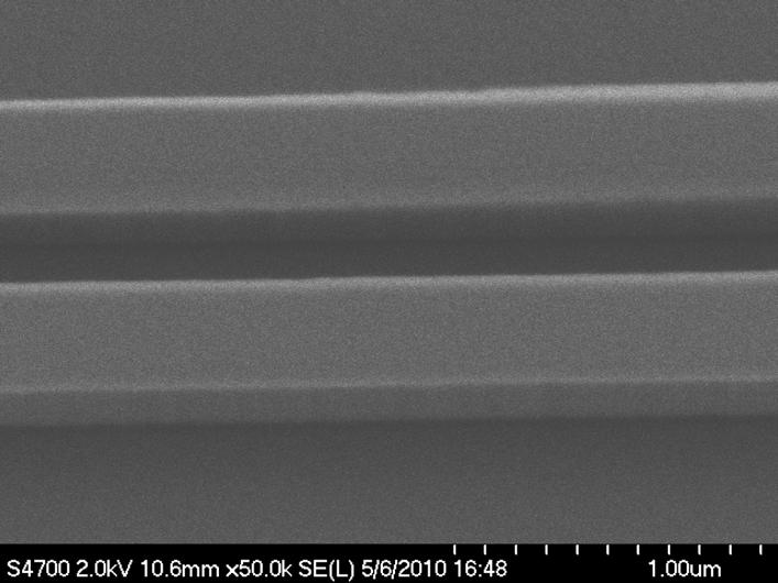
4 Fabricated Coupler 4
5 Two Methods: 1) Coupled-mode theory Find supermode effective indices, using: Lumerical mode solver calculate coupling 2) FDTD propagate a pulse down a coupler and observe power coupling 2D FDTD Effective Index Method 3D FDTD 5
6 Supermode Effective Index + Analytic Expression Find neff for the two supermodes (symmetric, anti-symmetric) Use coupler expressions to predict response Symmetric Anti-Symmetric Note: original single waveguide mode does not exist! It is only available via a superposition of the above two supermodes. 6

7 What is a supermode? A supermode is a mode of a super-structure, in this case, two waveguides. It is really an ordinary mode, and propagates just like any other mode: However, we can excite simultaneously 2 supermodes and observe interference (beating) 7
8 Directional Coupler Theory Cross-over length: L = 1sym 1asym = 0 2(n e 1sym n e 1asym ) Coupling coefficient (field), for a coupler with length Lc: r Pc apple = P 0 = sin 2 Lc L Assuming lossless coupling, the straight-through transmission amplitude coe cient is t = p 1 apple 2. However, if the couplers are lossy, then t 2 =1 apple 2 2, where 2 is a coe cient representing the existence of coupling losses.. 8

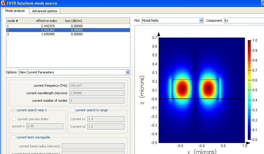
9 2D & 3D FDTD Mode Solver 9
10 Coupler calculations Question: Plot the mode profiles of the 2 guided modes. What are the effective indices? What is the cross-over coupler length? Cross-over length = distance after which the two super-modes are π shifted, 180º out of phase, i.e., ß1L-ß2L=π e.g. neff1 = , neff2 = Coupler cross-over length =1550e-9 / 2 / (neff1-neff2) = e-06 10
11 Mode profiles y Position [µm] x Position [µm] y Position [µm] x Position [µm]
12 Kappa vs. L apple = r Pc P 0 = sin 2 Lc L. Coupling power ratio Cross port (κ 2 ) Through port (t 2 ) Coupler Length [µm] 12
13 Cross-over length vs. Gap 3.5 x Cross over length [µm] Cross over length [µm] Coupler Gap [nm] Coupler Gap [nm] 13
14 Kappa vs. Gap (given L) apple = r Pc P 0 = sin 2 Lc L Field coupling, κ µm long coupler 15 µm long coupler Field coupling, κ Coupler Gap [nm] µm long coupler 15 µm long coupler Coupler Gap [nm] 14
15 Wavelength dependance Cross-over length Symmetric mode Antisymmetric mode Effective Index Cross over Length [µm] Wavelength [µm] Wavelength [µm] 15
16 Wavelength dependance Kappa µm long coupler 2 µm long coupler 5 µm long coupler Field coupling, κ Wavelength [µm] 16
17 Parasitic coupling 10 5 Coupler length [m] db coupling 30 db coupling 50 db coupling -50 db coupling for a 2 µm gap after 1 m! Coupler gap [µm] 17
18 Finite Difference Time Domain (FDTD) Modelling
19 What is FDTD? Exact numerical calculation of Maxwell s equations in the time domain Simulates pulses of light inside arbitrary geometries and materials Pulses of light contain many optical wavelength (short pulse = wide optical bandwidth, via Fourier Transform) A single pulse simulation provides response of the optical system for multiple wavelengths at once 19
20 FDTD Manuals FDTD_getting_started.pdf FDTD_reference_guide.pdf 20
21 FDTD Tutorial Waveguides


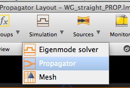
22 Lumerical MODE Propagator Uses Effective Index Method to collapse a 3D simulation into a 2D simulation Then performs a 2D FDTD simulation 22


23 Geometry 220x500 WG on oxide centred at y=0 Use Si-Palik 23
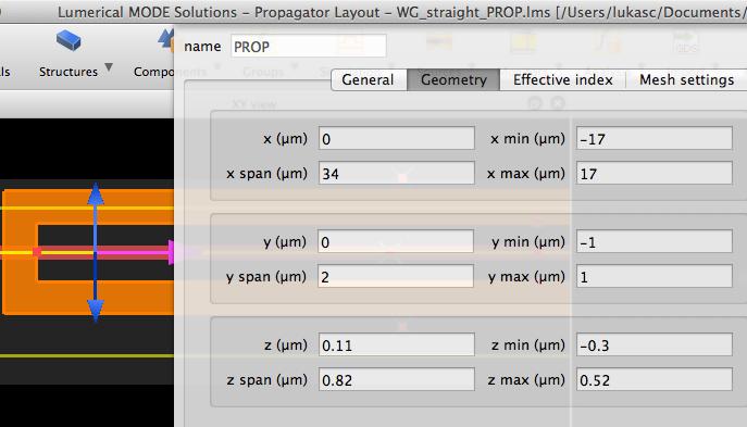
24 Simulation Volume 24


25 Mesh Settings Automatic mesh generation, with accurate conformal mesh. Auto non-uniform mesh Mesh Accuracy = 1 start with a very fast simulation to verify Mesh refinement conformal 25


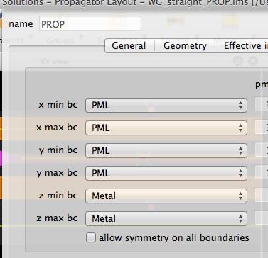
26 3D Simulation Volume Ensure that Si & SiO2 extend through PML. Leave 0.5 to 1 um around the waveguide. 26

27 MODE Propagator Effective Index Method 27
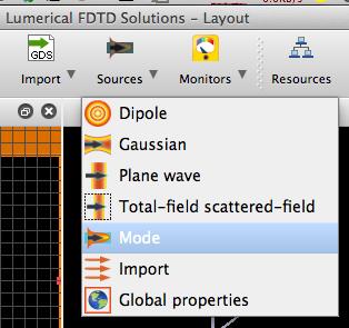
28 Mode Source Used to launch light into a waveguide. FDTD calculates the field distribution to match the guided optical mode of the waveguide. Calculation provides effective index of the optical mode. 28

29 Mode Source 29


30 Mode Source 3D FDTD Choose geometry, ensuring that mode source surrounds the waveguide. Choose injection axis, i.e. propagation direction Select Mode FDTD will calculate mode profile (with the mesh defined in FDTD simulation parameters). 30

31 3D Mode Source 3D FDTD Calculate Modes 31

32 Mode Profile, Effective Index 32


33 Mode Source PROP Choose geometry, ensuring that mode source surrounds the waveguide. Choose injection axis, i.e. propagation direction Select Mode PROP will calculate mode profile (with the mesh defined in FDTD simulation parameters). Or use Fundamental mode 33


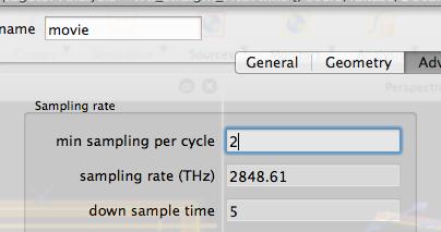
34 Movie monitor Speed up the movie: 34


35 Simulation Plot E vs. x in waveguide Plot transmission vs. wavelength at output of waveguide Watch movie 35
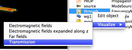
36 Simulation Transmission 36
37 Movie 37
38 Directional Couplers FDTD approach
39 FDTD Model Launch a pulse in one waveguide, model the pulse propagation Observe the power in each waveguide to determine the coupling coefficient study: wavelength dependance, gap dependance... Field profile, movie... 2D: use effective index method 3D: more time consuming, but more accurate includes bend regions 39
40 Coupling Lx=20.7;? sin(pi/2*l/lx)^2; 40


41 Effect of the bend region vs. 41

42 2D FDTD Structures Geometry Material index of refraction found from Mode Solver calculation for the SOI wafer slab, i.e. neff~ nm wide waveguides, 100 nm gap Bend regions: 42

43 2D FDTD Simulation Simulation region, x: PML, y: periodic dx=dy=40nm Mesh override in the two waveguides, dy=20 nm 43


44 2D FDTD Source Mode source Ensure that E-field is in y direction (i.e. TE-like) 44

45 2D FDTD Monitors Linear X Power Monitor 45
46 2D FDTD Results Plot monitor1, monitor2: Intensity vs. x Chose lambda ~ 1550 nm (closest for 5 freq. points is 1535 nm) x=getdata("monitor1","x"); y1=getdata("monitor1","ey"); y2=getdata("monitor2","ey"); plot (x,abs(y1(1:length(x),3))^2, abs(y2(1:length(x),3))^2, "x (um)"," E ^2"); Cross-over length: 20 um 46
47 2D FDTD Monitors Movie, 2D Power Monitor Movie & 2D Power Monitor of the entire structure Increases the simulation from ~10 s to ~1 minutes. 47

48 2D Power monitor at um What about other wavelengths? 48

49 2D Power monitor at 1.4 um: at 1.7 um: 49

50 Narrow band source Coupler is wavelength dependant Narrow-band source: 7 nm wide 1.55 um ~ THz 50


51 Coupler without bend region 51
52 Coupler without bend region Slight loss due to radiation 52


53 coupler2d_movie.fsp 2D FDTD Movies Note: large field in the gap 53

54 coupler2d_3db_v3.fsp Effect of the bend radius Sharp radius introduces losses by coupling the light into higher order modes of the waveguides. These modes have high losses (surface roughness). Increased bend radius reduces the coupler s losses. 54
 55")
55 Directional Coupler 3D FDTD Use a curved region (i.e. 2 nd waveguide comes in gradually ) Allow the input waveguide mode to gradually decompose into the two supermodes. Use silicon (3.48, or dispersive model) 55

56 3D FDTD Large field component in gap Coupling length ~ 30 um for wavelength = 1.54 um 56
57 Conclusions 2D FDTD 3D FDTD 2D MODE 3D MODE 2.5D MODE Propagator reasonably fast, good for tutorial example reasonably accurate, fast reasonably fast, reasonably accurate inaccurate slow inaccurate misses bend region effect EIM approximation 57

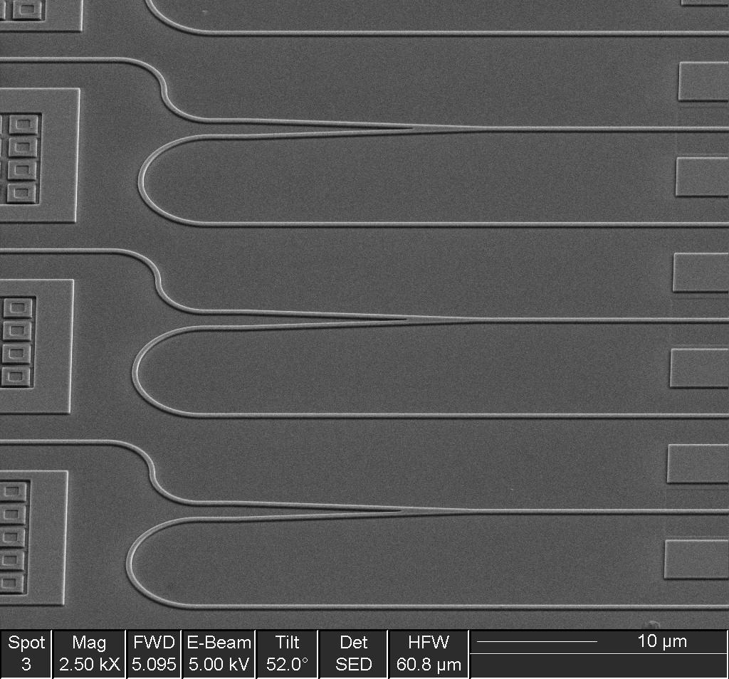
58 Directional coupler 200 nm gap, Ridge WG 58
 Through port (t 2 ) 2 2 0.2 0.1 L x = 16.")
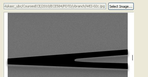
59 Experimental data Power Coupling apple 2 =sin [z + z bend ] 2L x t 2 =cos [z + z bend ] 2L x Cross port (κ 2 ) Through port (t 2 ) L x = 16.8 µm Z bend = 2.3 µm Coupler length [µm] 59
60 3D FDTD simulation Import GDS layout Setup FDTD simulation Vary structure parameter (e.g., length) Simulate each one Determine the through and cross coupling Plot coupling vs. Length Compare with experiments 60

61 DC_MODEprop.zip scripts to simulate coupler 61
62 Experiment vs. 3D FDTD Power Coupling apple 2 =sin [z + z bend ] 2L x t 2 =cos [z + z bend ] 2L x Through port (t 2 ) Cross port (κ 2 ) L x = 15.4 µm Z bend = 2.8 µm Coupler length [µm] 62
63 MODE vs. FDTD Field coupling, κ κ 2, 7.7 µm long coupler t 2, 7.7 µm long coupler κ 2, 5 µm long coupler, 3D FDTD t 2, 5 µm long coupler, 3D FDTD Coupler Gap [nm] 63
64 MODE vs. FDTD 10 1 Power coupling, κ 2, t κ 2, 5 µm long coupler, MODE κ 2, 7.7 µm long coupler, MODE t 2, 5 µm long coupler, MODE t 2, 7.7 µm long coupler, MODE κ 2, 5 µm long coupler, 3D FDTD t 2, 5 µm long coupler, 3D FDTD Coupler Gap [nm] 64
65 FDTD Tutorial Y-Branch Couplers
66 66

67 Fabricated Y-Branch splitter / coupler SEM image 6 between branches 67

68 Fabricated Y-Branch splitter / coupler FDTD can import SEM images; draw in black in the region of the coupler from SEM scale: 0.35 um um 44 nm 68


69 2D FDTD Import structure 69
 Auto mesh 6; PMLs (to absorb scattered light) Mode source, 1550 nm Monitors: Linear Y ( L, R ) and 2D")
70 2D FDTD Simulation Add input & output waveguides to match image data Effective index material (~2.8) Auto mesh 6; PMLs (to absorb scattered light) Mode source, 1550 nm Monitors: Linear Y ( L, R ) and 2D Power Monitors 70
,3),r(1:length(y),3),\"position, y\",\"power\" ); legend(\"left side\",\"right side\"); Almost a 50-50%")
71 2D FDTD Results at 1535 nm: L=getdata("monitorL","Px"); R=getdata("monitorR","Px"); y=getdata("monitorl","y"); plot(y,l(1:length(y),3),r(1:length(y),3),"position, y","power" ); legend("left side","right side"); Almost a 50-50% splitter. 71

72 FDTD Model Ideal layout Layout: 500 nm wide waveguides Each waveguide is rotated by 3 Separation of output waveguides is 500 nm In, Out1, Out2: Point Power Monitors, 200 frequency points. 72
73 Y-Branch Output Spectrum out1=pinch(getdata("out1","px"));out2=pinch(getdata("out2","px")); in=pinch(getdata("in","px")); f=getdata("out1","f"); plot(c/f,out1/in,out2/in,"wavelength","power" ); legend("output: Top","Output: Bottom"); 20 nm Mesh 10 nm Mesh 73

74 Y-Branch Movie 74
75 Y-Branch Combiner Reverse operation of a 50%-50% splitter In-phase sources (Gaussian, beam waist of 0.3 µm) constructive interference 180º out-of-phase sources (Gaussian, beam waist of 0.3 µm) destructive interference where does the power go? 75
Si-EPIC Workshop: Silicon Nanophotonics Fabrication Fibre Grating Couplers
 Si-EPIC Workshop: Silicon Nanophotonics Fabrication Fibre Grating Couplers June 30, 2012 Dr. Lukas Chrostowski Outline Coupling light to chips using Fibre Grating Couplers (FGC, or GC). Grating coupler
Index. Cambridge University Press Silicon Photonics Design Lukas Chrostowski and Michael Hochberg. Index.
 absorption, 69 active tuning, 234 alignment, 394 396 apodization, 164 applications, 7 automated optical probe station, 389 397 avalanche detector, 268 back reflection, 164 band structures, 30 bandwidth
CHAPTER 2 POLARIZATION SPLITTER- ROTATOR BASED ON A DOUBLE- ETCHED DIRECTIONAL COUPLER
 CHAPTER 2 POLARIZATION SPLITTER- ROTATOR BASED ON A DOUBLE- ETCHED DIRECTIONAL COUPLER As we discussed in chapter 1, silicon photonics has received much attention in the last decade. The main reason is
Waveguide Bragg Gratings and Resonators LUMERICAL SOLUTIONS INC
 Waveguide Bragg Gratings and Resonators JUNE 2016 1 Outline Introduction Waveguide Bragg gratings Background Simulation challenges and solutions Photolithography simulation Initial design with FDTD Band
SUPPLEMENTARY INFORMATION
 Supplementary Information S1. Theory of TPQI in a lossy directional coupler Following Barnett, et al. [24], we start with the probability of detecting one photon in each output of a lossy, symmetric beam
Directional coupler (2 Students)
") Directional coupler (2 Students) The goal of this project is to make a 2 by 2 optical directional coupler with a defined power ratio for the two output branches. The directional coupler should be optimized
Directional coupler (2 Students) The goal of this project is to make a 2 by 2 optical directional coupler with a defined power ratio for the two output branches. The directional coupler should be optimized
INTERNATIONAL JOURNAL OF PURE AND APPLIED RESEARCH IN ENGINEERING AND TECHNOLOGY
 INTERNATIONAL JOURNAL OF PURE AND APPLIED RESEARCH IN ENGINEERING AND TECHNOLOGY A PATH FOR HORIZING YOUR INNOVATIVE WORK ANALYSIS OF DIRECTIONAL COUPLER WITH SYMMETRICAL ADJACENT PARALLEL WAVEGUIDES USING
Design and Simulation of Optical Power Splitter By using SOI Material
 J. Pure Appl. & Ind. Phys. Vol.3 (3), 193-197 (2013) Design and Simulation of Optical Power Splitter By using SOI Material NAGARAJU PENDAM * and C P VARDHANI 1 * Research Scholar, Department of Physics,
Multimode Interference Waveguides
 Multimode Interference Waveguides Jesus Perez Mechanical Engineering Major Santa Barbara City College Mentor: Akhilesh Khope Faculty Advisor: John Bowers ECE Department Why Integrated Photonics? Vast potential
Numerical Analysis and Optimization of a Multi-Mode Interference Polarization Beam Splitter
 Numerical Analysis and Optimization of a Multi-Mode Interference Polarization Beam Splitter Y. D Mello*, J. Skoric, M. Hui, E. Elfiky, D. Patel, D. Plant Department of Electrical Engineering, McGill University,
Optical Polarization Filters and Splitters Based on Multimode Interference Structures using Silicon Waveguides
 International Journal of Engineering and Technology Volume No. 7, July, 01 Optical Polarization Filters and Splitters Based on Multimode Interference Structures using Silicon Waveguides 1 Trung-Thanh Le,
Design, Simulation & Optimization of 2D Photonic Crystal Power Splitter
 Optics and Photonics Journal, 2013, 3, 13-19 http://dx.doi.org/10.4236/opj.2013.32a002 Published Online June 2013 (http://www.scirp.org/journal/opj) Design, Simulation & Optimization of 2D Photonic Crystal
Polarization Splitting Rotator (PSR) based on Sub-Wavelength Grating (SWG) waveguides
 based on Sub-Wavelength Grating (SWG) waveguides") Polarization Splitting Rotator (PSR) based on Sub-Wavelength Grating (SWG) waveguides Oscar Yun Wang Dr. Lukas Chrostowski Ref. Textbook: L. Chrostowski, M. Hochberg, Silicon Photonics Design, Cambridge
Polarization Splitting Rotator (PSR) based on Sub-Wavelength Grating (SWG) waveguides Oscar Yun Wang Dr. Lukas Chrostowski Ref. Textbook: L. Chrostowski, M. Hochberg, Silicon Photonics Design, Cambridge
Compact two-mode (de)multiplexer based on symmetric Y-junction and Multimode interference waveguides
multiplexer based on symmetric Y-junction and Multimode interference waveguides") Compact two-mode (de)multiplexer based on symmetric Y-junction and Multimode interference waveguides Yaming Li, Chong Li, Chuanbo Li, Buwen Cheng, * and Chunlai Xue State Key Laboratory on Integrated Optoelectronics,
Compact two-mode (de)multiplexer based on symmetric Y-junction and Multimode interference waveguides Yaming Li, Chong Li, Chuanbo Li, Buwen Cheng, * and Chunlai Xue State Key Laboratory on Integrated Optoelectronics,
Arbitrary Power Splitting Couplers Based on 3x3 Multimode Interference Structures for All-optical Computing
 Arbitrary Power Splitting Couplers Based on 3x3 Multimode Interference Structures for All-optical Computing Trung-Thanh Le Abstract--Chip level optical links based on VLSI photonic integrated circuits
SUPPLEMENTARY INFORMATION
 SUPPLEMENTARY INFORMATION doi:0.038/nature727 Table of Contents S. Power and Phase Management in the Nanophotonic Phased Array 3 S.2 Nanoantenna Design 6 S.3 Synthesis of Large-Scale Nanophotonic Phased
Ultracompact and low power optical switch based on silicon. photonic crystals
 Ultracompact and low power optical switch based on silicon photonic crystals Daryl M. Beggs 1, *, Thomas P. White 1, Liam O Faolain 1 and Thomas F. Krauss 1 1 School of Physics and Astronomy, University
Variable splitting ratio 2 2 MMI couplers using multimode waveguide holograms
 Variable splitting ratio 2 2 MMI couplers using multimode waveguide holograms Shuo-Yen Tseng, Canek Fuentes-Hernandez, Daniel Owens, and Bernard Kippelen Center for Organic Photonics and Electronics, School
GoToWebinar Housekeeping: attendee screen Lumerical Solutions, Inc.
 GoToWebinar Housekeeping: attendee screen 2012 Lumerical Solutions, Inc. GoToWebinar Housekeeping: your participation Open and hide your control panel Join audio: Choose Mic & Speakers to use VoIP Choose
Supplementary information for Stretchable photonic crystal cavity with
 Supplementary information for Stretchable photonic crystal cavity with wide frequency tunability Chun L. Yu, 1,, Hyunwoo Kim, 1, Nathalie de Leon, 1,2 Ian W. Frank, 3 Jacob T. Robinson, 1,! Murray McCutcheon,
Microphotonics Readiness for Commercial CMOS Manufacturing. Marco Romagnoli
 Microphotonics Readiness for Commercial CMOS Manufacturing Marco Romagnoli MicroPhotonics Consortium meeting MIT, Cambridge October 15 th, 2012 Passive optical structures based on SOI technology Building
OPTI510R: Photonics. Khanh Kieu College of Optical Sciences, University of Arizona Meinel building R.626
 OPTI510R: Photonics Khanh Kieu College of Optical Sciences, University of Arizona kkieu@optics.arizona.edu Meinel building R.626 Announcements Homework #3 is due today No class Monday, Feb 26 Pre-record
Virtual EM Prototyping: From Microwaves to Optics
 Virtual EM Prototyping: From Microwaves to Optics Dr. Frank Demming, CST AG Dr. Avri Frenkel, Anafa Electromagnetic Solutions Virtual EM Prototyping Efficient Maxwell Equations solvers has been developed,
Silicon Photonic Device Based on Bragg Grating Waveguide
 Silicon Photonic Device Based on Bragg Grating Waveguide Hwee-Gee Teo, 1 Ming-Bin Yu, 1 Guo-Qiang Lo, 1 Kazuhiro Goi, 2 Ken Sakuma, 2 Kensuke Ogawa, 2 Ning Guan, 2 and Yong-Tsong Tan 2 Silicon photonics
Title. Author(s)Fujisawa, Takeshi; Koshiba, Masanori. CitationOptics Letters, 31(1): Issue Date Doc URL. Rights. Type.
Fujisawa, Takeshi; Koshiba, Masanori. CitationOptics Letters, 31(1): Issue Date Doc URL. Rights. Type.") Title Polarization-independent optical directional coupler Author(s)Fujisawa, Takeshi; Koshiba, Masanori CitationOptics Letters, 31(1): 56-58 Issue Date 2006 Doc URL http://hdl.handle.net/2115/948 Rights
Title Polarization-independent optical directional coupler Author(s)Fujisawa, Takeshi; Koshiba, Masanori CitationOptics Letters, 31(1): 56-58 Issue Date 2006 Doc URL http://hdl.handle.net/2115/948 Rights
Polarization Analysis of an Asymmetrically Etched Rib Waveguide Coupler for Sensing Applications
 Photonic Sensors (2013) Vol. 3, No. 2: 178 183 DOI: 10.1007/s13320-013-0079-6 Regular Photonic Sensors Polarization Analysis of an Asymmetrically Etched Rib Waveguide Coupler for Sensing Applications Malathi
Strong-Field-Enhanced Spectroscopy in Silicon. Nanoparticle Electric and Magnetic Dipole. Resonance near a Metal Surface
 Supplementary Information Strong-Field-Enhanced Spectroscopy in Silicon Nanoparticle Electric and Magnetic Dipole Resonance near a Metal Surface Zengli Huang, Jianfeng Wang, *, Zhenghui Liu, Gengzhao Xu,
Compact hybrid TM-pass polarizer for silicon-on-insulator platform
 Compact hybrid TM-pass polarizer for silicon-on-insulator platform Muhammad Alam,* J. Stewart Aitchsion, and Mohammad Mojahedi Department of Electrical and Computer Engineering, University of Toronto,
Lateral leakage of TM-like mode in thin-ridge Silicon-on-Insulator bent waveguides and ring resonators
 Lateral leakage of TM-like mode in thin-ridge Silicon-on-Insulator bent waveguides and ring resonators Thach G. Nguyen *, Ravi S. Tummidi 2, Thomas L. Koch 2, and Arnan Mitchell School of Electrical and
Waveguiding in PMMA photonic crystals
 ROMANIAN JOURNAL OF INFORMATION SCIENCE AND TECHNOLOGY Volume 12, Number 3, 2009, 308 316 Waveguiding in PMMA photonic crystals Daniela DRAGOMAN 1, Adrian DINESCU 2, Raluca MÜLLER2, Cristian KUSKO 2, Alex.
Silicon photonic devices based on binary blazed gratings
 Silicon photonic devices based on binary blazed gratings Zhiping Zhou Li Yu Optical Engineering 52(9), 091708 (September 2013) Silicon photonic devices based on binary blazed gratings Zhiping Zhou Li Yu
FIBER OPTICS. Prof. R.K. Shevgaonkar. Department of Electrical Engineering. Indian Institute of Technology, Bombay. Lecture: 29.
 FIBER OPTICS Prof. R.K. Shevgaonkar Department of Electrical Engineering Indian Institute of Technology, Bombay Lecture: 29 Integrated Optics Fiber Optics, Prof. R.K. Shevgaonkar, Dept. of Electrical Engineering,
Tunable Color Filters Based on Metal-Insulator-Metal Resonators
 Chapter 6 Tunable Color Filters Based on Metal-Insulator-Metal Resonators 6.1 Introduction In this chapter, we discuss the culmination of Chapters 3, 4, and 5. We report a method for filtering white light
Horizontal single and multiple slot waveguides: optical transmission at λ = 1550 nm
 Horizontal single and multiple slot waveguides: optical transmission at λ = 1550 nm Rong Sun 1 *, Po Dong 2 *, Ning-ning Feng 1, Ching-yin Hong 1, Jurgen Michel 1, Michal Lipson 2, Lionel Kimerling 1 1Department
Plane wave excitation by taper array for optical leaky waveguide antenna
 LETTER IEICE Electronics Express, Vol.15, No.2, 1 6 Plane wave excitation by taper array for optical leaky waveguide antenna Hiroshi Hashiguchi a), Toshihiko Baba, and Hiroyuki Arai Graduate School of
Finite-Difference Time-Domain and Beam Propagation Methods for Maxwell s Equations: Demonstrations with BeamPROP / FullWAVE
 Finite-Difference Time-Domain and Beam Propagation Methods for Maxwell s Equations: Demonstrations with BeamPROP / FullWAVE Wolfgang Freude and Jan Brosi Institute of High-Frequency and Quantum Electronics
Supplementary Figures
 Supplementary Figures Supplementary Figure 1 EM wave transport through a 150 bend. (a) Bend of our PEC-PMC waveguide. (b) Bend of the conventional PEC waveguide. Waves are incident from the lower left
Chapter 10 WDM concepts and components
 Chapter 10 WDM concepts and components - Outline 10.1 Operational principle of WDM 10. Passive Components - The x Fiber Coupler - Scattering Matrix Representation - The x Waveguide Coupler - Mach-Zehnder
Fiber Optic Communications Communication Systems
 INTRODUCTION TO FIBER-OPTIC COMMUNICATIONS A fiber-optic system is similar to the copper wire system in many respects. The difference is that fiber-optics use light pulses to transmit information down
Multimode Optical Fiber
 Multimode Optical Fiber 1 OBJECTIVE Determine the optical modes that exist for multimode step index fibers and investigate their performance on optical systems. 2 PRE-LAB The backbone of optical systems
Electro-Optic Modulators Workshop
 Electro-Optic Modulators Workshop NUSOD 2013 Outline New feature highlights Electro-optic modulators Circuit level view Modulator categories Component simulation and parameter extraction Electro-optic
Numerical Analysis and Optimization of a Multi-Mode Interference Based Polarization Beam Splitter
 Numerical Analysis and Optimization of a Multi-Mode Interference Based Polarization Beam Splitter Yannick D Mello* 1, James Skoric 1, Eslam Elfiky 1, Michael Hui 1, David Patel 1, Yun Wang 1, and David
Workshop on Coherent Phenomena in Disordered Optical Systems May Slow-light Propagation in Photonic Nano-Structures
 2583-15 Workshop on Coherent Phenomena in Disordered Optical Systems 26-30 May 2014 Slow-light Propagation in Photonic Nano-Structures Jin HOU College of Electronics & Information Engineering, South-Central
Two bit optical analog-to-digital converter based on photonic crystals
 Two bit optical analog-to-digital converter based on photonic crystals Binglin Miao, Caihua Chen, Ahmed Sharkway, Shouyuan Shi, and Dennis W. Prather University of Delaware, Newark, Delaware 976 binglin@udel.edu
Absorption: in an OF, the loss of Optical power, resulting from conversion of that power into heat.
 Absorption: in an OF, the loss of Optical power, resulting from conversion of that power into heat. Scattering: The changes in direction of light confined within an OF, occurring due to imperfection in
Supplementary Figure 1. GO thin film thickness characterization. The thickness of the prepared GO thin
 Supplementary Figure 1. GO thin film thickness characterization. The thickness of the prepared GO thin film is characterized by using an optical profiler (Bruker ContourGT InMotion). Inset: 3D optical
Modeling Fabrication Non-Uniformity in Chip-Scale Silicon Photonic Interconnects
 Modeling Fabrication Non-Uniformity in Chip-Scale Silicon Photonic Interconnects Mahdi Nikdast,3, Gabriela Nicolescu, Jelena Trajkovic 2, and Odile Liboiron-Ladouceur 3 Polytechnique Montréal, Montréal,
Supplementary Figure 1 Reflective and refractive behaviors of light with normal
 Supplementary Figures Supplementary Figure 1 Reflective and refractive behaviors of light with normal incidence in a three layer system. E 1 and E r are the complex amplitudes of the incident wave and
Hybrid Integration Technology of Silicon Optical Waveguide and Electronic Circuit
 Hybrid Integration Technology of Silicon Optical Waveguide and Electronic Circuit Daisuke Shimura Kyoko Kotani Hiroyuki Takahashi Hideaki Okayama Hiroki Yaegashi Due to the proliferation of broadband services
UC Santa Barbara UC Santa Barbara Previously Published Works
 UC Santa Barbara UC Santa Barbara Previously Published Works Title Compact broadband polarizer based on shallowly-etched silicon-on-insulator ridge optical waveguides Permalink https://escholarship.org/uc/item/959523wq
City, University of London Institutional Repository
 City Research Online City, University of London Institutional Repository Citation: Dhingra, N., Song, J., Ghosh, S. ORCID: 0000-0002-1992-2289, Zhou, L. and Rahman, B. M. A. ORCID: 0000-0001-6384-0961
Electromagnetically Induced Transparency with Hybrid Silicon-Plasmonic Travelling-Wave Resonators
 XXI International Workshop on Optical Wave & Waveguide Theory and Numerical Modelling 19-20 April 2013 Enschede, The Netherlands Session: Nanophotonics Electromagnetically Induced Transparency with Hybrid
ECE 6323 Ridge Waveguide Laser homework
 ECE 633 Ridge Waveguide Laser homework Introduction This is a slide from a lecture we will study later on. It is about diode lasers. Although we haven t studied diode lasers, there is one aspect about
Dual Vivaldi UWB nanoantenna for optical applications
 Dual Vivaldi UWB nanoantenna for optical applications Zeev Iluz, Yuval Yifat, Doron Bar-Lev, Michal Eitan, Yoni Kantarovsky, Yuav Blue, Yael Hanein, Koby Scheuer, and Amir Boag School of Electrical Engineering
CHIRPED FIBER BRAGG GRATING (CFBG) BY ETCHING TECHNIQUE FOR SIMULTANEOUS TEMPERATURE AND REFRACTIVE INDEX SENSING
 BY ETCHING TECHNIQUE FOR SIMULTANEOUS TEMPERATURE AND REFRACTIVE INDEX SENSING") CHIRPED FIBER BRAGG GRATING (CFBG) BY ETCHING TECHNIQUE FOR SIMULTANEOUS TEMPERATURE AND REFRACTIVE INDEX SENSING Siti Aisyah bt. Ibrahim and Chong Wu Yi Photonics Research Center Department of Physics,
CHIRPED FIBER BRAGG GRATING (CFBG) BY ETCHING TECHNIQUE FOR SIMULTANEOUS TEMPERATURE AND REFRACTIVE INDEX SENSING Siti Aisyah bt. Ibrahim and Chong Wu Yi Photonics Research Center Department of Physics,
Design and fabrication of indium phosphide air-bridge waveguides with MEMS functionality
 Design and fabrication of indium phosphide air-bridge waveguides with MEMS functionality Wing H. Ng* a, Nina Podoliak b, Peter Horak b, Jiang Wu a, Huiyun Liu a, William J. Stewart b, and Anthony J. Kenyon
DBR based passively mode-locked 1.5m semiconductor laser with 9 nm tuning range Moskalenko, V.; Williams, K.A.; Bente, E.A.J.M.
 DBR based passively mode-locked 1.5m semiconductor laser with 9 nm tuning range Moskalenko, V.; Williams, K.A.; Bente, E.A.J.M. Published in: Proceedings of the 20th Annual Symposium of the IEEE Photonics
MICRO RING MODULATOR. Dae-hyun Kwon. High-speed circuits and Systems Laboratory
 MICRO RING MODULATOR Dae-hyun Kwon High-speed circuits and Systems Laboratory Paper preview Title of the paper Low Vpp, ultralow-energy, compact, high-speed silicon electro-optic modulator Publication
Characterization of Photonic Structures with CST Microwave Studio. CST UGM 2010 Darmstadt
 Characterization of Photonic Structures with CST Microwave Studio Stefan Prorok, Jan Hendrik Wülbern, Jan Hampe, Hooi Sing Lee, Alexander Petrov and Manfred Eich, Institute of Optical and Electronic Materials
The Effect of Radiation Coupling in Higher Order Fiber Bragg Gratings
 PIERS ONLINE, VOL. 3, NO. 4, 27 462 The Effect of Radiation Coupling in Higher Order Fiber Bragg Gratings Li Yang 1, Wei-Ping Huang 2, and Xi-Jia Gu 3 1 Department EEIS, University of Science and Technology
z t h l g 2009 John Wiley & Sons, Inc. Published 2009 by John Wiley & Sons, Inc.
 x w z t h l g Figure 10.1 Photoconductive switch in microstrip transmission-line geometry: (a) top view; (b) side view. Adapted from [579]. Copyright 1983, IEEE. I g G t C g V g V i V r t x u V t Z 0 Z
Supporting Information: Achromatic Metalens over 60 nm Bandwidth in the Visible and Metalens with Reverse Chromatic Dispersion
 Supporting Information: Achromatic Metalens over 60 nm Bandwidth in the Visible and Metalens with Reverse Chromatic Dispersion M. Khorasaninejad 1*, Z. Shi 2*, A. Y. Zhu 1, W. T. Chen 1, V. Sanjeev 1,3,
 Chapter 5 5.1 What are the factors that determine the thickness of a polystyrene waveguide formed by spinning a solution of dissolved polystyrene onto a substrate? density of polymer concentration of polymer
Four wave mixing and parametric amplification in Si-nano waveguides using reverse biased pnjunctions
 Four wave mixing and parametric amplification in Si-nano waveguides using reverse biased pnjunctions for carrier removal E-Mail: petermann@tu-berlin.de Acknowledgements A.Gajda 1, G.Winzer 1, L.Zimmermann
CHAPTER 2 MICROSTRIP REFLECTARRAY ANTENNA AND PERFORMANCE EVALUATION
 43 CHAPTER 2 MICROSTRIP REFLECTARRAY ANTENNA AND PERFORMANCE EVALUATION 2.1 INTRODUCTION This work begins with design of reflectarrays with conventional patches as unit cells for operation at Ku Band in
THE PROBLEM of electromagnetic interference between
 IEEE TRANSACTIONS ON ELECTROMAGNETIC COMPATIBILITY, VOL. 50, NO. 2, MAY 2008 399 Estimation of Current Distribution on Multilayer Printed Circuit Board by Near-Field Measurement Qiang Chen, Member, IEEE,
some aspects of Optical Coherence Tomography
 some aspects of Optical Coherence Tomography SSOM Lectures, Engelberg 17.3.2009 Ch. Meier 1 / 34 Contents 1. OCT - basic principles (Time Domain Frequency Domain) 2. Performance and limiting factors 3.
Supplementary Figure 1. Effect of the spacer thickness on the resonance properties of the gold and silver metasurface layers.
 Supplementary Figure 1. Effect of the spacer thickness on the resonance properties of the gold and silver metasurface layers. Finite-difference time-domain calculations of the optical transmittance through
Ti: LiNbO 3 Acousto-Optic Tunable Filter (AOTF)
") UDC 621.372.54:621.391.6 Ti: LiNbO 3 Acousto-Optic Tunable Filter (AOTF) VTadao Nakazawa VShinji Taniguchi VMinoru Seino (Manuscript received April 3, 1999) We have developed the following new elements
UDC 621.372.54:621.391.6 Ti: LiNbO 3 Acousto-Optic Tunable Filter (AOTF) VTadao Nakazawa VShinji Taniguchi VMinoru Seino (Manuscript received April 3, 1999) We have developed the following new elements
Fully-Etched Grating Coupler with Low Back Reflection
 Fully-Etched Grating Coupler with Low Back Reflection Yun Wang a, Wei Shi b, Xu Wang a, Jonas Flueckiger a, Han Yun a, Nicolas A. F. Jaeger a, and Lukas Chrostowski a a The University of British Columbia,
Integrated into Nanowire Waveguides
 Supporting Information Widely Tunable Distributed Bragg Reflectors Integrated into Nanowire Waveguides Anthony Fu, 1,3 Hanwei Gao, 1,3,4 Petar Petrov, 1, Peidong Yang 1,2,3* 1 Department of Chemistry,
arxiv:physics/ v1 [physics.optics] 28 Sep 2005
![arxiv:physics/ v1 [physics.optics] 28 Sep 2005](/thumbs/91/105523130.jpg "arxiv:physics/ v1 [physics.optics] 28 Sep 2005") Near-field enhancement and imaging in double cylindrical polariton-resonant structures: Enlarging perfect lens Pekka Alitalo, Stanislav Maslovski, and Sergei Tretyakov arxiv:physics/0509232v1 [physics.optics]
Near-field enhancement and imaging in double cylindrical polariton-resonant structures: Enlarging perfect lens Pekka Alitalo, Stanislav Maslovski, and Sergei Tretyakov arxiv:physics/0509232v1 [physics.optics]
Fibre Optic Sensors: basic principles and most common applications
 SMR 1829-21 Winter College on Fibre Optics, Fibre Lasers and Sensors 12-23 February 2007 Fibre Optic Sensors: basic principles and most common applications (PART 2) Hypolito José Kalinowski Federal University
THE WIDE USE of optical wavelength division multiplexing
 1322 IEEE JOURNAL OF QUANTUM ELECTRONICS, VOL. 35, NO. 9, SEPTEMBER 1999 Coupling of Modes Analysis of Resonant Channel Add Drop Filters C. Manolatou, M. J. Khan, Shanhui Fan, Pierre R. Villeneuve, H.
Nano Structure Based Power Splitter Design by Using 2D Photonic Crystals
 Journal of Modern Science and Technology Vol. 1. No. 1. May 2013 Issue. Pp.176-187 Nano Structure Based Power Splitter Design by Using 2D Photonic Crystals Md. Masruf Khan A nanostructure (80-100 μm 2
20dB-enhanced coupling to slot photonic crystal waveguide based on. multimode interference
 20dB-enhanced coupling to slot photonic crystal waveguide based on multimode interference Xiaonan Chen 1, Lanlan Gu 2, Wei Jiang 2, and Ray T. Chen 1* Microelectronic Research Center, Department of Electrical
Projects in microwave theory 2009
 Electrical and information technology Projects in microwave theory 2009 Write a short report on the project that includes a short abstract, an introduction, a theory section, a section on the results and
Guided Propagation Along the Optical Fiber
 Guided Propagation Along the Optical Fiber The Nature of Light Quantum Theory Light consists of small particles (photons) Wave Theory Light travels as a transverse electromagnetic wave Ray Theory Light
The Design of Optical Signal Transforms Based on Planar Waveguides on a Silicon on Insulator Platform
 IACSIT International Journal of Engineering and Technology, Vol., No.3, June ISSN: 793-836 The Design of Optical Signal Transforms Based on Planar Waveguides on a Silicon on Insulator Platform Trung-Thanh
- no emitters/amplifiers available. - complex process - no CMOS-compatible
 Advantages of photonic integrated circuits (PICs) in Microwave Photonics (MWP): compactness low-power consumption, stability flexibility possibility of aggregating optics and electronics functionalities
Deliverable Report. Deliverable No: D2.9 Deliverable Title: OAM waveguide transmission
 Deliverable Report Deliverable No: D2.9 Deliverable Title: OAM waveguide transmission Grant Agreement number: 255914 Project acronym: PHORBITECH Project title: A Toolbox for Photon Orbital Angular Momentum
CHAPTER 4 RESULTS. 4.1 Introduction
 CHAPTER 4 RESULTS 4.1 Introduction In this chapter focus are given more on WDM system. The results which are obtained mainly from the simulation work are presented. In simulation analysis, the study will
MICRORING resonators (MRRs) are often presented as
 are often presented as") JOURNAL OF LIGHTWAVE TECHNOLOGY, VOL. 36, NO. 13, JULY 1, 018 767 Design Space Exploration of Microring Resonators in Silicon Photonic Interconnects: Impact of the Ring Curvature Meisam Bahadori, Student
JOURNAL OF LIGHTWAVE TECHNOLOGY, VOL. 36, NO. 13, JULY 1, 018 767 Design Space Exploration of Microring Resonators in Silicon Photonic Interconnects: Impact of the Ring Curvature Meisam Bahadori, Student
Design and Analysis of Resonant Leaky-mode Broadband Reflectors
 846 PIERS Proceedings, Cambridge, USA, July 6, 8 Design and Analysis of Resonant Leaky-mode Broadband Reflectors M. Shokooh-Saremi and R. Magnusson Department of Electrical and Computer Engineering, University
Optical Fiber Technology. Photonic Network By Dr. M H Zaidi
 Optical Fiber Technology Numerical Aperture (NA) What is numerical aperture (NA)? Numerical aperture is the measure of the light gathering ability of optical fiber The higher the NA, the larger the core
Development of a LFLE Double Pattern Process for TE Mode Photonic Devices. Mycahya Eggleston Advisor: Dr. Stephen Preble
 Development of a LFLE Double Pattern Process for TE Mode Photonic Devices Mycahya Eggleston Advisor: Dr. Stephen Preble 2 Introduction and Motivation Silicon Photonics Geometry, TE vs TM, Double Pattern
and smart design tools Even though James Clerk Maxwell derived his famous set of equations around the year 1865,
 Smart algorithms and smart design tools Even though James Clerk Maxwell derived his famous set of equations around the year 1865, solving them to accurately predict the behaviour of light remains a challenge.
A thin foil optical strain gage based on silicon-on-insulator microresonators
 A thin foil optical strain gage based on silicon-on-insulator microresonators D. Taillaert* a, W. Van Paepegem b, J. Vlekken c, R. Baets a a Photonics research group, Ghent University - INTEC, St-Pietersnieuwstraat
Slot waveguide-based splitters for broadband terahertz radiation
 Slot waveguide-based splitters for broadband terahertz radiation Shashank Pandey, Gagan Kumar, and Ajay Nahata* Department of Electrical and Computer Engineering, University of Utah, Salt Lake City, Utah
Projects in microwave theory 2017
 Electrical and information technology Projects in microwave theory 2017 Write a short report on the project that includes a short abstract, an introduction, a theory section, a section on the results and
ALMA MEMO #360 Design of Sideband Separation SIS Mixer for 3 mm Band
 ALMA MEMO #360 Design of Sideband Separation SIS Mixer for 3 mm Band V. Vassilev and V. Belitsky Onsala Space Observatory, Chalmers University of Technology ABSTRACT As a part of Onsala development of
Supporting Information: Plasmonic and Silicon Photonic Waveguides
 Supporting Information: Efficient Coupling between Dielectric-Loaded Plasmonic and Silicon Photonic Waveguides Ryan M. Briggs, *, Jonathan Grandidier, Stanley P. Burgos, Eyal Feigenbaum, and Harry A. Atwater,
An Example Design using the Analog Photonics Component Library. 3/21/2017 Benjamin Moss
 An Example Design using the Analog Photonics Component Library 3/21/2017 Benjamin Moss Component Library Elements Passive Library Elements: Component Current specs 1 Edge Couplers (Si)
Active Device Utilities and Multi-Level Simulation An Overview
 Active Device Utilities and Multi-Level Simulation An Overview If you have technical questions, please contact evanh@synopsys.com 2016 Synopsys, Inc. 1 Outline Introduction Multi-Physics Utility Carrier
Chapter 1 Silicon Photonic Wire Waveguides: Fundamentals and Applications
 Chapter 1 Silicon Photonic Wire Waveguides: Fundamentals and Applications Koji Yamada Abstract This chapter reviews the fundamental characteristics and basic applications of the silicon photonic wire waveguide.
DISPERSION MEASUREMENT FOR ON-CHIP MICRORESONATOR. A Thesis. Submitted to the Faculty. Purdue University. Steven Chen. In Partial Fulfillment of the
 i DISPERSION MEASUREMENT FOR ON-CHIP MICRORESONATOR A Thesis Submitted to the Faculty of Purdue University by Steven Chen In Partial Fulfillment of the Requirements for the Degree of Master of Science
Properties of Structured Light
 Properties of Structured Light Gaussian Beams Structured light sources using lasers as the illumination source are governed by theories of Gaussian beams. Unlike incoherent sources, coherent laser sources
Diffractive optical elements for high gain lasers with arbitrary output beam profiles
 Diffractive optical elements for high gain lasers with arbitrary output beam profiles Adam J. Caley, Martin J. Thomson 2, Jinsong Liu, Andrew J. Waddie and Mohammad R. Taghizadeh. Heriot-Watt University,
Design of TE and TM Mode Mach-Zehnder Interferometer based on SOI Technology
 1 Design of TE and TM Mode Mach-Zehnder Interferometer based on SOI Technology Sourangsu Banerji, Department of Electronics & Communication Engineering, RCC-Institute of Information Technology Abstract
Resonator.
 The New Design and Simulation of an Optical Add Drop Filter Based On Hexagonal Photonic Crystal Single Ring Race Track Resonator Abolfazl Abbaspour ', Hamed Alipour Banaei2, Alireza Andalib 2 Student of