»ULTRASURFACE«ULTRA DYNAMIC OPTICAL SYSTEMS FOR HIGH THROUGHPUT LASER SURFACE PROCESSING. ultra SURFACE
|
|
|
- Claud Watkins
- 5 years ago
- Views:
Transcription


1 »ULTRASURFACE«ULTRA DYNAMIC OPTICAL SYSTEMS FOR HIGH THROUGHPUT LASER SURFACE PROCESSING ultra SURFACE
2 AGENDA Motivation & goal of the ultrasurface project Project relevant technologies Concept & approach First results General information about the beneficiary & role in the project - 2 -
3 AGENDA Motivation & goal of the ultrasurface project Project relevant technologies Concept & approach First results General information about the beneficiary & role in the project - 3 -
4 Motivation Surface processing techniques are widely used in industry Laser based processes offer high flexibility, precision and quality offer new possibilities for creating complex surfaces The throughput of these processes is often not sufficient for an economic, industrial application In the same time: Laser sources getting more and more affordable - 4 -
5 Goal Overall goal: Increase the throughput of laser based surface treatment processes by a factor of 10 Project title:»ultra Dynamic Optical Systems for High Throughput Laser Surface Processing«- 5 -
6 AGENDA Motivation & goal of the ultrasurface project Project relevant technologies Concept & approach First results General information about the beneficiary & role in the project - 6 -

7 Laser processes Laser structuring (LS) Achieve small structures in micrometre scale With each pulse a tiny amount of material is removed by ablation Processing of 3D parts is achieved by sequential processing of tiles The low throughput is still limiting this technique to the processing of moulds rather than the processing of the work piece itself / individual parts - 7 -

8 Laser processes Laser polishing (LP) Based on remelting a thin surface layer and smoothing the surface due to the surface tension Initial roughness of Ra = 1 10 µm can be reduced down to Ra = µm Process has been adapted to 3D parts for a circular shaped beam profile In-house developed 3D CAM-NC process chain allows the processing of complex 3D parts using simultaneous processing First industrial applications already showed the potential of this new technology while the throughput is still one of the main limitations - 8 -
 Tool for improving")

9 Laser processes Laser thin-film processing (LT) Tool for improving the performance of technical components e.g. wear, corrosion protection or electrical conductivity Often a 2-step process involving the deposition of the film followed by a heat treatment Lasers represent a versatile alternative to conventional heat treatment: processing of thermally sensitive substrates, defined local treatment of a component In many fields of application requires long processing times and not adapted for complex 3D components yet - 9 -
")
 For almost")

10 Laser processes All processes A laser scanner is used for a fast (v>10 m/s) beam deflection in 2D/3D Laser scanner Focusing lens (f-theta) For almost every application a circular shaped beam profile is used Gaussian Top-Hat
 The shape of continuous")

11 Optical elements Piezoelectric deformable mirrors (PDM) The shape of continuous faceplate is deformed by piezoceramic (PZT) actuators working on transverse piezoeffect

 Low cost")


 19 to 109")
12 Optical elements Piezoelectric deformable mirrors (PDM) Low cost actuators Free edge Can be coated with all available coatings (up to 1 kw load) Response: 1.5 khz Correction range (8 um per actuator) 19 to 109 actuators 30 and 50 mm apertures
 1.")


 Image")
 DOE MultiS")

13 Optical elements Diffractive optical element (DOE) 1. Using diffraction and interference phenomenons Holoor designs a special pattern for a desired result 2. The special pattern is applied over a substrate to create the DOE using a lithography process(es) Image by Lookang (Wikipedia) Image by Peo (Wikipedia) DOE MultiS pot 3. The DOE is implemented into a system to achieve desired or improved output


 Beam")


14 Optical elements Diffractive optical element (DOE) Beam splitting Beam shaping Beam focal shaping Others: sampling, phase corrections
15 AGENDA Motivation & goal of the ultrasurface project Project relevant technologies Concept & approach First results General information about the beneficiary & role in the project
16 Concept & approach Increasing throughput State of the art Circular or square intensity distributions Meandering tool path v dy Troughput: Laser structuring v TP = t npt + -> Multiple beams for parallel processing A v dy n Laser Compensating heat losses at 1 the edge t npt non-prod. Time A -> Increase n Laser Laser polishing v Low intensity High intensity Melting Heat treatmeant -> Process adapted Area intensity distributions v -> Velocity Increase v and dy dy Track offset n Laser # Laser Laser thin-film proc. Drying Sintering v v dy
17 Concept & approach Multi-beam, beam-shaping State of the art Circular or square intensity distributions Meandering tool path v dy Laser structuring v -> Multiple beams for parallel processing -> Increase n Laser Laser polishing v Low intensity High intensity -> Process adapted intensity distributions -> Increase v and dy Compensating heat losses at the edge Melting Heat treatmeant Laser thin-film proc. Drying Sintering v v dy
18 Concept & approach Adaptive beam-shaping for 2D/3D processing Perpendicular angle of incidence NON-perpendicular angle of incidence State of the art Processing conditions change with angle of incidence Adaption of intensity distribution within 1 ms Adaptive distortion of intensity distribution by dynamic optics -> f(b) Constant processing conditions b

19 Concept & approach Adaptive multi-beam positioning for 2D/3D processing
20 Concept & approach S.M.A.R.T. objectives»ultra Dynamic Optical Systems for High Throughput Laser Surface Processing«SO1 - Dynamic and flexible beam-shaping optics for laser surface processing SO2 - Multi-beam optics for parallel laser surface processing SO3 - Ultrafast synchronisation of optics and machine for 3D processing SO4 - Validation in industrial scenarios
21 AGENDA Motivation & goal of the ultrasurface project Project relevant technologies Concept & approach First results General information about the beneficiary & role in the project
: additional (static) beam-shaping element required - 22")
22 Beam-Shaping Optics (SO1) - Concept Analytical model for deformable mirror (PDM) shape PDM surface shape is calculated based on actuator voltages and integrated into optical design software evaluation of beam-shaping capabilities of state-of-the-art PDMs results for 79 channel piezo-electric DM (ᴓ 50 mm): additional (static) beam-shaping element required
 PDM compensates for scanner and 3D-surface related")
23 Beam-Shaping Optics (SO1) - Concept Adapted concept: beam is pre-shaped with a rotatable diffractive optical element (DOE) PDM compensates for scanner and 3D-surface related distortions


24 Beam-Shaping Optics (SO1) - Realization Software Process control CAM Data Management Laser Source Galvanometer Deformable Mirror Focus shifter Hollow Shaft Motor DOE Controller


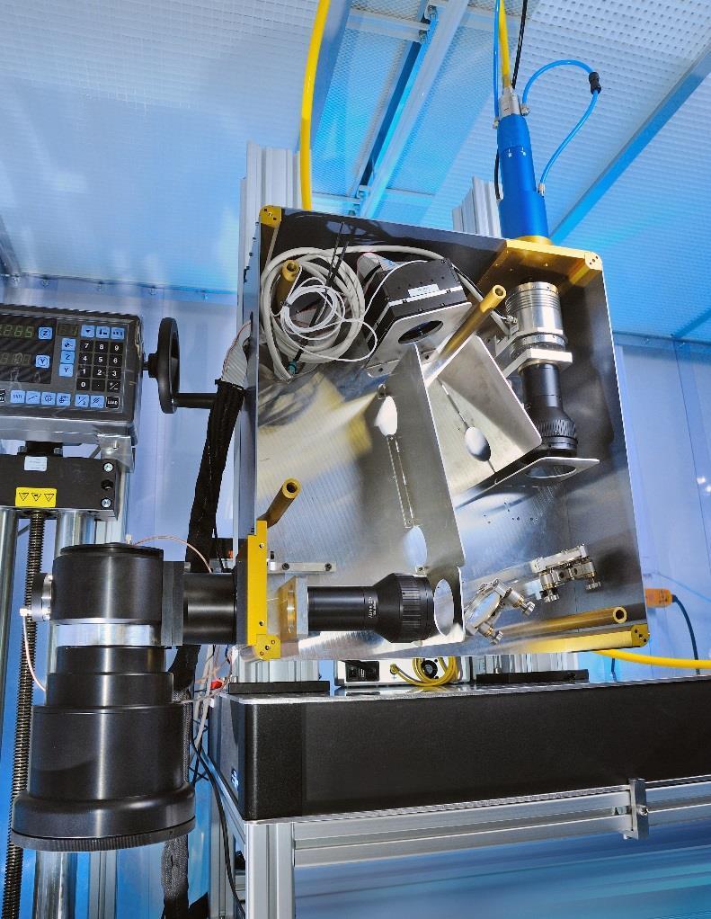
25 Beam-Shaping Optics (SO1) - Realization PDM DOE
26 Multi-Beam Optics (SO2) - Concept f-theta 2nd relay work piece spot position control unit intermediate focus 1st relay DOE DOE (diffractive optical element) splits initial beam into separate beams 1 st relay lens focuses light into intermediate focus 2 nd relay lens images DOE into scanner Spot position control unit for individual beam positioning

 Distortion of spot array for large")
27 Multi-Beam Optics (SO2) - Spot Position Control Unit Independent x-, y- and z-positioning of each beam z: miniaturized focus shifter for each beam (+/- 3.5 mm) x + y: 2 rotatable plane-parallel glass plates per beam (+/- 400 µm) Compensation of: Local surface tilt (>10 ) Distortion of spot array for large scan angles

28 Multi-Beam Optics (SO2) - Spot Position Control Unit focus shifters miniaturized servomotor fused silica plates scanner motor 100 mm


29 Multi-Beam Optics (SO2) - Realization Software Process control CAM Data Management Spot control unit Laser Source DOE Controller

30 Machine Tool (SO3) - Concept Mechanical engineering 5 numerical axis granite base measurement probe integrated Utilities (electrical, pneumatics, safety,...) protective atmosphere suitable laser safety housing

31 Machine Tool (SO3) - Realization
32 AGENDA Motivation & goal of the ultrasurface project Project relevant technologies Concept & approach First results General information about the beneficiary & role in the project
33 Consortium
34 Contacts & role in the project FHG-ILT: project coordination, process development for laser polishing, laser thin film processing and laser micro structuring Project coordination: Dr. Edgar Willenborg phone: Laser polishing: Judith Kumstel phone: Laser thin film processing: Hendrik Sändker phone: Laser structuring: Dr. Johannes Finger phone:
35 Contacts & role in the project RWTH-TOS: Development of beam-shaping and multi-beam optics Oskar Hofmann, phone: UNITECH: Development and construction of the machine Ivan Calderon, phone: PULSAR: Optics assembly and characterization Dr. Stephan Eifel phone: NEWSON: Development of scanner systems Kathrin Delay phone:
36 Contacts & role in the project OKO: Development of deformable mirrors Seva Patlan phone: HOLO-OR: Development of DOEs Natan Kaplan Procter&Gamble P&G: End user Klaus Eimann SCHAEFFLER: End user Joachim Weber GEMÜ: End user Andreas Schönpflug
Beam Shaping and Simultaneous Exposure by Diffractive Optical Element in Laser Plastic Welding
 Beam Shaping and Simultaneous Exposure by Diffractive Optical Element in Laser Plastic Welding AKL`12 9th May 2012 Dr. Daniel Vogler Page 1 Motivation: Quality and flexibility diffractive spot shaping
Beam deflection technologies for ultra short pulse lasers June 5th, 2018
 Beam deflection technologies for ultra short pulse lasers June 5th, 2018 Agenda SCANLAB GmbH XL Scan excellishift precsys 2 SCANLAB at a Glance Worldwide leading OEM manufacturer of scan solutions for
POCKET DEFORMABLE MIRROR FOR ADAPTIVE OPTICS APPLICATIONS
 POCKET DEFORMABLE MIRROR FOR ADAPTIVE OPTICS APPLICATIONS Leonid Beresnev1, Mikhail Vorontsov1,2 and Peter Wangsness3 1) US Army Research Laboratory, 2800 Powder Mill Road, Adelphi Maryland 20783, lberesnev@arl.army.mil,
Nmark AGV-HP. High Accuracy, Thermally Stable Galvo Scanner
 Nmark AGV-HP Galvanometer Nmark AGV-HP High Accuracy, Thermally Stable Galvo Scanner Highest accuracy scanner available attains single-digit, micron-level accuracy over the field of view Optical feedback
Development of a Deformable Mirror for High-Power Lasers
 Development of a Deformable Mirror for High-Power Lasers Dr. Justin Mansell and Robert Praus MZA Associates Corporation Mirror Technology Days August 1, 2007 1 Outline Introduction & Project Goal Deformable
Nmark AGV-HPO. High Accuracy, Open Frame, Thermally Stable Galvo Scanner. Highest accuracy scanner available attains singledigit,
 Nmark AGV-HPO Galvanometer Nmark AGV-HPO High Accuracy, Open Frame, Thermally Stable Galvo Scanner Highest accuracy scanner available attains singledigit, micron-level accuracy over the field of view Optical
Optical Components for Laser Applications. Günter Toesko - Laserseminar BLZ im Dezember
 Günter Toesko - Laserseminar BLZ im Dezember 2009 1 Aberrations An optical aberration is a distortion in the image formed by an optical system compared to the original. It can arise for a number of reasons
OPTICS IN MOTION. Introduction: Competing Technologies: 1 of 6 3/18/2012 6:27 PM.
 1 of 6 3/18/2012 6:27 PM OPTICS IN MOTION STANDARD AND CUSTOM FAST STEERING MIRRORS Home Products Contact Tutorial Navigate Our Site 1) Laser Beam Stabilization to design and build a custom 3.5 x 5 inch,
Nmark AGV-HP. High Accuracy, Thermally Stable Galvo Scanner
 Nmark AGV-HP High Accuracy, Thermally Stable Galvo Scanner Highest accuracy scanner available attains single-digit, micron-level accuracy over the field of view Optical feedback technology significantly
plasmonic nanoblock pair
 Nanostructured potential of optical trapping using a plasmonic nanoblock pair Yoshito Tanaka, Shogo Kaneda and Keiji Sasaki* Research Institute for Electronic Science, Hokkaido University, Sapporo 1-2,
Adaptive optics for laser-based manufacturing processes
 Adaptive optics for laser-based manufacturing processes Rainer Beck 1, Jon Parry 1, Rhys Carrington 1,William MacPherson 1, Andrew Waddie 1, Derryck Reid 1, Nick Weston 2, Jon Shephard 1, Duncan Hand 1
ADALAM Sensor based adaptive laser micromachining using ultrashort pulse lasers for zero-failure manufacturing D2.2. Ger Folkersma (Demcon)
") D2.2 Automatic adjustable reference path system Document Coordinator: Contributors: Dissemination: Keywords: Ger Folkersma (Demcon) Ger Folkersma, Kevin Voss, Marvin Klein (Demcon) Public Reference path,
D2.2 Automatic adjustable reference path system Document Coordinator: Contributors: Dissemination: Keywords: Ger Folkersma (Demcon) Ger Folkersma, Kevin Voss, Marvin Klein (Demcon) Public Reference path,
Nmark AGV-HP(O) High Accuracy, Thermally Stable Galvo Scanner
 High Accuracy, Thermally Stable Galvo Scanner") Nmark AGV-HP(O) Galvanometer Nmark AGV-HP(O) High Accuracy, Thermally Stable Galvo Scanner Highest accuracy scanner available attains single-digit, micron-level accuracy over the field of view Optical
Nmark AGV-HP(O) Galvanometer Nmark AGV-HP(O) High Accuracy, Thermally Stable Galvo Scanner Highest accuracy scanner available attains single-digit, micron-level accuracy over the field of view Optical
Nmark AGV-HP(O) High Accuracy, Thermally Stable Galvo Scanner
 High Accuracy, Thermally Stable Galvo Scanner") Nmark AGV-HP(O) High Accuracy, Thermally Stable Galvo Scanner Highest accuracy scanner available attains single-digit, micron-level accuracy over the field of view Optical feedback technology significantly
Nmark AGV-HP(O) High Accuracy, Thermally Stable Galvo Scanner Highest accuracy scanner available attains single-digit, micron-level accuracy over the field of view Optical feedback technology significantly
Practical Applications of Laser Technology for Semiconductor Electronics
 Practical Applications of Laser Technology for Semiconductor Electronics MOPA Single Pass Nanosecond Laser Applications for Semiconductor / Solar / MEMS & General Manufacturing Mark Brodsky US Application
MEMS for RF, Micro Optics and Scanning Probe Nanotechnology Applications
 MEMS for RF, Micro Optics and Scanning Probe Nanotechnology Applications Part I: RF Applications Introductions and Motivations What are RF MEMS? Example Devices RFIC RFIC consists of Active components
Rear Side Processing of Soda-Lime Glass Using DPSS Nanosecond Laser
 Lasers in Manufacturing Conference 215 Rear Side Processing of Soda-Lime Glass Using DPSS Nanosecond Laser Juozas Dudutis*, Paulius Gečys, Gediminas Račiukaitis Center for Physical Sciences and Technology,
OPTICS DIVISION B. School/#: Names:
 OPTICS DIVISION B School/#: Names: Directions: Fill in your response for each question in the space provided. All questions are worth two points. Multiple Choice (2 points each question) 1. Which of the
Experiment 1: Fraunhofer Diffraction of Light by a Single Slit
 Experiment 1: Fraunhofer Diffraction of Light by a Single Slit Purpose 1. To understand the theory of Fraunhofer diffraction of light at a single slit and at a circular aperture; 2. To learn how to measure
Diffractive Axicon application note
 Diffractive Axicon application note. Introduction 2. General definition 3. General specifications of Diffractive Axicons 4. Typical applications 5. Advantages of the Diffractive Axicon 6. Principle of
Laser Beam Analysis Using Image Processing
 Journal of Computer Science 2 (): 09-3, 2006 ISSN 549-3636 Science Publications, 2006 Laser Beam Analysis Using Image Processing Yas A. Alsultanny Computer Science Department, Amman Arab University for
AgilOptics mirrors increase coupling efficiency into a 4 µm diameter fiber by 750%.
 Application Note AN004: Fiber Coupling Improvement Introduction AgilOptics mirrors increase coupling efficiency into a 4 µm diameter fiber by 750%. Industrial lasers used for cutting, welding, drilling,
UV EXCIMER LASER BEAM HOMOGENIZATION FOR MICROMACHINING APPLICATIONS
 Optics and Photonics Letters Vol. 4, No. 2 (2011) 75 81 c World Scientific Publishing Company DOI: 10.1142/S1793528811000226 UV EXCIMER LASER BEAM HOMOGENIZATION FOR MICROMACHINING APPLICATIONS ANDREW
Titelfoto. Advanced Laser Beam Shaping - for Optimized Process Results and Quality Inspection in the PV Production - Maja Thies.
 2010 LIMO Lissotschenko Mikrooptik GmbH www.limo.de Titelfoto Advanced Laser Beam Shaping - for Optimized Process Results and Quality Inspection in the PV Production - Maja Thies Photonics Key Technology
USER MANUAL VarioS-Microscanner-Demonstrators
 FRAUNHOFER INSTITUTE FOR PHOTONIC MICROSYSTEMS IPMS USER MANUAL VarioS-Microscanner-Demonstrators last revision : 2014-11-14 [Fb046.08] USER MANUAL.doc Introduction Thank you for purchasing a VarioS-microscanner-demonstrator
New techniques for laser micromachining MEMS devices
 New techniques for laser micromachining MEMS devices Charles Abbott, Ric Allott, Bob Bann, Karl Boehlen, Malcolm Gower, Phil Rumsby, Ines Stassen- Boehlen and Neil Sykes Exitech Ltd, Oxford Industrial
Conditions for the dynamic control of the focusing properties of the high power cw CO 2 laser beam in a system with an adaptive mirror
 Conditions for the dynamic control of the focusing properties of the high power cw CO 2 laser beam in a system with an adaptive mirror G. Rabczuk 1, M. Sawczak Institute of Fluid Flow Machinery, Polish
LASER TECHNOLOGY. Key parameters. Groundbreaking in the laser processing of cutting tools. A member of the UNITED GRINDING Group
 Creating Tool Performance A member of the UNITED GRINDING Group Groundbreaking in the laser processing of cutting tools Key parameters The machining of modern materials using laser technology knows no
1.6 Beam Wander vs. Image Jitter
 8 Chapter 1 1.6 Beam Wander vs. Image Jitter It is common at this point to look at beam wander and image jitter and ask what differentiates them. Consider a cooperative optical communication system that
SENSOR+TEST Conference SENSOR 2009 Proceedings II
 B8.4 Optical 3D Measurement of Micro Structures Ettemeyer, Andreas; Marxer, Michael; Keferstein, Claus NTB Interstaatliche Hochschule für Technik Buchs Werdenbergstr. 4, 8471 Buchs, Switzerland Introduction
Instructions for the Experiment
 Instructions for the Experiment Excitonic States in Atomically Thin Semiconductors 1. Introduction Alongside with electrical measurements, optical measurements are an indispensable tool for the study of
Precise hardening with high power diode lasers using beam shaping mirror optics
 Precise hardening with high power diode lasers using beam shaping mirror optics Steffen Bonss, Marko Seifert, Berndt Brenner, Eckhard Beyer Fraunhofer IWS, Winterbergstrasse 28, D-01277 Dresden, Germany
Characteristics of point-focus Simultaneous Spatial and temporal Focusing (SSTF) as a two-photon excited fluorescence microscopy
 as a two-photon excited fluorescence microscopy") Characteristics of point-focus Simultaneous Spatial and temporal Focusing (SSTF) as a two-photon excited fluorescence microscopy Qiyuan Song (M2) and Aoi Nakamura (B4) Abstracts: We theoretically and experimentally
Characteristics of point-focus Simultaneous Spatial and temporal Focusing (SSTF) as a two-photon excited fluorescence microscopy Qiyuan Song (M2) and Aoi Nakamura (B4) Abstracts: We theoretically and experimentally
CHAPTER 7. Waveguide writing in optimal conditions. 7.1 Introduction
 CHAPTER 7 7.1 Introduction In this chapter, we want to emphasize the technological interest of controlled laser-processing in dielectric materials. Since the first report of femtosecond laser induced refractive
Diffuser / Homogenizer - diffractive optics
 Diffuser / Homogenizer - diffractive optics Introduction Homogenizer (HM) product line can be useful in many applications requiring a well-defined beam shape with a randomly-diffused intensity profile.
Precision machining and measurement of micro aspheric molds
 Precision machining and measurement of micro aspheric molds H. Suzuki 1,3, T. Moriwaki 2,. amagata 3, and T. Higuchi 4 1 Chubu University, Kasugai, Aichi, Japan 2 Setsunan University, Neyagawa, Osaka,
Silicon Light Machines Patents
 820 Kifer Road, Sunnyvale, CA 94086 Tel. 408-240-4700 Fax 408-456-0708 www.siliconlight.com Silicon Light Machines Patents USPTO No. US 5,808,797 US 5,841,579 US 5,798,743 US 5,661,592 US 5,629,801 US
Supplementary Information
 Supplementary Information Supplementary Figure 1. Modal simulation and frequency response of a high- frequency (75- khz) MEMS. a, Modal frequency of the device was simulated using Coventorware and shows
Adaptive Optics for LIGO
 Adaptive Optics for LIGO Justin Mansell Ginzton Laboratory LIGO-G990022-39-M Motivation Wavefront Sensor Outline Characterization Enhancements Modeling Projections Adaptive Optics Results Effects of Thermal
MEASUREMENT APPLICATION GUIDE OUTER/INNER
 MEASUREMENT APPLICATION GUIDE OUTER/INNER DIAMETER Measurement I N D E X y Selection Guide P.2 y Measurement Principle P.3 y P.4 y X and Y Axes Synchronous Outer Diameter Measurement P.5 y of a Large Diameter
Laser Speckle Reducer LSR-3000 Series
 Datasheet: LSR-3000 Series Update: 06.08.2012 Copyright 2012 Optotune Laser Speckle Reducer LSR-3000 Series Speckle noise from a laser-based system is reduced by dynamically diffusing the laser beam. A
Novel Beam Diagnostics Improve Laser Additive Manufacturing
 A Coherent Whitepaper November 17, 2016 Novel Beam Diagnostics Improve Laser Additive Manufacturing Laser additive manufacturing (LAM) is rapidly becoming an important method for the fabrication of both
FemtoFAB. Femtosecond laser micromachining system. tel fax Konstitucijos ave. 23C LT Vilnius, Lithuania
 FemtoFAB Femtosecond laser micromachining system Konstitucijos ave. 23C LT-08105 Vilnius, Lithuania tel. +370 5 272 57 38 fax +370 5 272 37 04 info@wophotonics.com www.wophotonics.com INTRODUCTION FemtoFAB
Novel Beam Diagnostics Improve Laser Additive Manufacturing
 White Paper Novel Beam Diagnostics Improve Laser Additive Manufacturing Laser additive manufacturing (LAM) is rapidly becoming an important method for the fabrication of both prototype and production metal
Measurement of Surface Profile and Layer Cross-section with Wide Field of View and High Precision
 Hitachi Review Vol. 65 (2016), No. 7 243 Featured Articles Measurement of Surface Profile and Layer Cross-section with Wide Field of View and High Precision VS1000 Series Coherence Scanning Interferometer
The RSH Catalogue. Laser Optics & Lenses
 The RSH Catalogue Laser Optics & Lenses 2013 2014 1 Company Profile RSH Optronics, Headquartered in Ajmer, Rajasthan, India, is the leading supplier & manufacturer for Photonics Products (Optics, Laser
Ultrafast Lasers with Radial and Azimuthal Polarizations for Highefficiency. Applications
 WP Ultrafast Lasers with Radial and Azimuthal Polarizations for Highefficiency Micro-machining Applications Beneficiaries Call Topic Objective ICT-2013.3.2 Photonics iii) Laser for Industrial processing
Fiber Optic Communications
 Fiber Optic Communications ( Chapter 2: Optics Review ) presented by Prof. Kwang-Chun Ho 1 Section 2.4: Numerical Aperture Consider an optical receiver: where the diameter of photodetector surface area
Lithography. 3 rd. lecture: introduction. Prof. Yosi Shacham-Diamand. Fall 2004
 Lithography 3 rd lecture: introduction Prof. Yosi Shacham-Diamand Fall 2004 1 List of content Fundamental principles Characteristics parameters Exposure systems 2 Fundamental principles Aerial Image Exposure
attocfm I for Surface Quality Inspection NANOSCOPY APPLICATION NOTE M01 RELATED PRODUCTS G
 APPLICATION NOTE M01 attocfm I for Surface Quality Inspection Confocal microscopes work by scanning a tiny light spot on a sample and by measuring the scattered light in the illuminated volume. First,
Use of Computer Generated Holograms for Testing Aspheric Optics
 Use of Computer Generated Holograms for Testing Aspheric Optics James H. Burge and James C. Wyant Optical Sciences Center, University of Arizona, Tucson, AZ 85721 http://www.optics.arizona.edu/jcwyant,
Optical Components - Scanning Lenses
 Optical Components Scanning Lenses Scanning Lenses (Ftheta) Product Information Figure 1: Scanning Lenses A scanning (Ftheta) lens supplies an image in accordance with the socalled Ftheta condition (y
ESCC2006 European Supply Chain Convention
 ESCC2006 European Supply Chain Convention PCB Paper 20 Laser Technology for cutting FPC s and PCB s Mark Hüske, Innovation Manager, LPKF Laser & Electronics AG, Germany Laser Technology for cutting FPCs
Advances in Laser Micro-machining for Wafer Probing and Trimming
 Advances in Laser Micro-machining for Wafer Probing and Trimming M.R.H. Knowles, A.I.Bell, G. Rutterford & A. Webb Oxford Lasers June 10, 2002 Oxford Lasers June 2002 1 Introduction to Laser Micro-machining
ADVANCED OPTICS LAB -ECEN Basic Skills Lab
 ADVANCED OPTICS LAB -ECEN 5606 Basic Skills Lab Dr. Steve Cundiff and Edward McKenna, 1/15/04 Revised KW 1/15/06, 1/8/10 Revised CC and RZ 01/17/14 The goal of this lab is to provide you with practice
Theory and Applications of Frequency Domain Laser Ultrasonics
 1st International Symposium on Laser Ultrasonics: Science, Technology and Applications July 16-18 2008, Montreal, Canada Theory and Applications of Frequency Domain Laser Ultrasonics Todd W. MURRAY 1,
Excimer laser projector for microelectronics applications
 Excimer laser projector for microelectronics applications P T Rumsby and M C Gower Exitech Ltd Hanborough Park, Long Hanborough, Oxford OX8 8LH, England ABSTRACT Fully integrated excimer laser mask macro
Compact and Reliable Speckle Reduction
 Compact and Reliable Speckle Reduction August 2017 Mark Ventura, Vice President Sales & Marketing Optotune Switzerland AG Bernstrasse 388 CH-8953 Dietikon Switzerland Phone +41 58 856 3011 www.optotune.com
Micro- and Nano-Technology... for Optics
 Micro- and Nano-Technology...... for Optics 3.2 Lithography U.D. Zeitner Fraunhofer Institut für Angewandte Optik und Feinmechanik Jena Printing on Stones Map of Munich Stone Print Contact Printing light
648. Measurement of trajectories of piezoelectric actuators with laser Doppler vibrometer
 648. Measurement of trajectories of piezoelectric actuators with laser Doppler vibrometer V. Grigaliūnas, G. Balčiūnas, A.Vilkauskas Kaunas University of Technology, Kaunas, Lithuania E-mail: valdas.grigaliunas@ktu.lt
Near-field Optical Microscopy
 Near-field Optical Microscopy R. Fernandez, X. Wang, N. Li, K. Parker, and A. La Rosa Physics Department Portland State University Portland, Oregon Near-Field SPIE Optics Microscopy East 2005 Group PSU
Dark Field Technologies In-Situ Defect Detection Practical Considerations and Results
 Dark Field Technologies In-Situ Defect Detection Practical Considerations and Results June 21, 2017 In-Situ Defect Detection The need for In-Situ Defect Detection Solid State Laser Reflection Practical
Surface Finish Measurement Methods and Instrumentation
 125 years of innovation Surface Finish Measurement Methods and Instrumentation Contents Visual Inspection Surface Finish Comparison Plates Contact Gauges Inductive / Variable Reluctance (INTRA) Piezo Electric
White Paper: Modifying Laser Beams No Way Around It, So Here s How
 White Paper: Modifying Laser Beams No Way Around It, So Here s How By John McCauley, Product Specialist, Ophir Photonics There are many applications for lasers in the world today with even more on the
Mirrors. Plano and Spherical. Mirrors. Published on II-VI Infrared
 Page 1 of 13 Published on II-VI Infrared Plano and Spherical or total reflectors are used in laser cavities as rear reflectors and fold mirrors, and externally as beam benders in beam delivery systems.
EUV Plasma Source with IR Power Recycling
 1 EUV Plasma Source with IR Power Recycling Kenneth C. Johnson kjinnovation@earthlink.net 1/6/2016 (first revision) Abstract Laser power requirements for an EUV laser-produced plasma source can be reduced
PicoMaster 100. Unprecedented finesse in creating 3D micro structures. UV direct laser writer for maskless lithography
 UV direct laser writer for maskless lithography Unprecedented finesse in creating 3D micro structures Highest resolution in the market utilizing a 405 nm diode laser Structures as small as 300 nm 375 nm
Proposed Adaptive Optics system for Vainu Bappu Telescope
 Proposed Adaptive Optics system for Vainu Bappu Telescope Essential requirements of an adaptive optics system Adaptive Optics is a real time wave front error measurement and correction system The essential
BMC s heritage deformable mirror technology that uses hysteresis free electrostatic
 Optical Modulator Technical Whitepaper MEMS Optical Modulator Technology Overview The BMC MEMS Optical Modulator, shown in Figure 1, was designed for use in free space optical communication systems. The
7. Michelson Interferometer
 7. Michelson Interferometer In this lab we are going to observe the interference patterns produced by two spherical waves as well as by two plane waves. We will study the operation of a Michelson interferometer,
Smart off axis absolute position sensor solution and UTAF piezo motor enable closed loop control of a miniaturized Risley prism pair
 Smart off axis absolute position sensor solution and UTAF piezo motor enable closed loop control of a miniaturized Risley prism pair By David Cigna and Lisa Schaertl, New Scale Technologies Hall effect
Outline: Introduction: What is SPM, history STM AFM Image treatment Advanced SPM techniques Applications in semiconductor research and industry
 1 Outline: Introduction: What is SPM, history STM AFM Image treatment Advanced SPM techniques Applications in semiconductor research and industry 2 Back to our solutions: The main problem: How to get nm
High-speed Fabrication of Micro-channels using Line-based Laser Induced Plasma Micromachining (L-LIPMM)
") Proceedings of the 8th International Conference on MicroManufacturing University of Victoria, Victoria, BC, Canada, March 25-28, 2013 High-speed Fabrication of Micro-channels using Line-based Laser Induced
Proceedings of the 8th International Conference on MicroManufacturing University of Victoria, Victoria, BC, Canada, March 25-28, 2013 High-speed Fabrication of Micro-channels using Line-based Laser Induced
CANUNDA. Application note. Flexible high-power laser beam shaping.
 CANUNDA Application note Flexible high-power laser beam shaping www.cailabs.com CONTENT INTRODUCTION LASER BEAM SHAPING SOLUTIONS 5 7 Multimode laser beam shaping Singlemode laser beam shaping and combining
EE119 Introduction to Optical Engineering Spring 2003 Final Exam. Name:
 EE119 Introduction to Optical Engineering Spring 2003 Final Exam Name: SID: CLOSED BOOK. THREE 8 1/2 X 11 SHEETS OF NOTES, AND SCIENTIFIC POCKET CALCULATOR PERMITTED. TIME ALLOTTED: 180 MINUTES Fundamental
Lecture 22 Optical MEMS (4)
") EEL6935 Advanced MEMS (Spring 2005) Instructor: Dr. Huikai Xie Lecture 22 Optical MEMS (4) Agenda: Refractive Optical Elements Microlenses GRIN Lenses Microprisms Reference: S. Sinzinger and J. Jahns,
EEL6935 Advanced MEMS (Spring 2005) Instructor: Dr. Huikai Xie Lecture 22 Optical MEMS (4) Agenda: Refractive Optical Elements Microlenses GRIN Lenses Microprisms Reference: S. Sinzinger and J. Jahns,
Adaptive optics and high power pulse lasers
 Adaptive optics and high power pulse lasers Alexis Kudryashov, Alexander Alexandrov, Valentina Zavalova, Alexey Rukosuev, Vadim Samarkin Shatura Branch Moscow State Open University Adaptive Optics Lab.
Improving efficiency of CO 2
 Improving efficiency of CO 2 Laser System for LPP Sn EUV Source K.Nowak*, T.Suganuma*, T.Yokotsuka*, K.Fujitaka*, M.Moriya*, T.Ohta*, A.Kurosu*, A.Sumitani** and J.Fujimoto*** * KOMATSU ** KOMATSU/EUVA
Sinusoidal wavelength-scanning common-path interferometer with a beam-scanning system for measurement of film thickness variations
 Sinusoidal wavelength-scanning common-path interferometer with a beam-scanning system for measurement of film thickness variations Osami Sasaki, Takafumi Morimatsu, Samuel Choi, and Takamasa Suzuki Faculty
Principles of Optics for Engineers
 Principles of Optics for Engineers Uniting historically different approaches by presenting optical analyses as solutions of Maxwell s equations, this unique book enables students and practicing engineers
Point Autofocus Probe Surface Texture Measuring Instrument. PF-60 technical report
 Point Autofocus Probe Surface Texture Measuring Instrument PF-60 technical report ISO approved Mitaka measuring method for areal surface texture (ISO 25178-605) Document No, Title Published ISO 25178-6
NEW LASER ULTRASONIC INTERFEROMETER FOR INDUSTRIAL APPLICATIONS B.Pouet and S.Breugnot Bossa Nova Technologies; Venice, CA, USA
 NEW LASER ULTRASONIC INTERFEROMETER FOR INDUSTRIAL APPLICATIONS B.Pouet and S.Breugnot Bossa Nova Technologies; Venice, CA, USA Abstract: A novel interferometric scheme for detection of ultrasound is presented.
Design and test of a high-contrast imaging coronagraph based on two. 50-step transmission filters
 Design and test of a high-contrast imaging coronagraph based on two 50-step transmission filters Jiangpei Dou *a,b, Deqing Ren a,b,c, Yongtian Zhu a,b, Xi Zhang a,b,d, Xue Wang a,b,d a. National Astronomical
Photolithography II ( Part 2 )
") 1 Photolithography II ( Part 2 ) Chapter 14 : Semiconductor Manufacturing Technology by M. Quirk & J. Serda Saroj Kumar Patra, Department of Electronics and Telecommunication, Norwegian University of Science
1 Photolithography II ( Part 2 ) Chapter 14 : Semiconductor Manufacturing Technology by M. Quirk & J. Serda Saroj Kumar Patra, Department of Electronics and Telecommunication, Norwegian University of Science
Radial Polarization Converter With LC Driver USER MANUAL
 ARCoptix Radial Polarization Converter With LC Driver USER MANUAL Arcoptix S.A Ch. Trois-portes 18 2000 Neuchâtel Switzerland Mail: info@arcoptix.com Tel: ++41 32 731 04 66 Principle of the radial polarization
Intra-cavity active optics in lasers
 Intra-cavity active optics in lasers W. Lubeigt, A. Kelly, V. Savitsky, D. Burns Institute of Photonics, University of Strathclyde Wolfson Centre,106 Rottenrow Glasgow G4 0NW, UK J. Gomes, G. Brown, D.
MicroSpot FOCUSING OBJECTIVES
 OFR P R E C I S I O N O P T I C A L P R O D U C T S MicroSpot FOCUSING OBJECTIVES APPLICATIONS Micromachining Microlithography Laser scribing Photoablation MAJOR FEATURES For UV excimer & high-power YAG
Physics 431 Final Exam Examples (3:00-5:00 pm 12/16/2009) TIME ALLOTTED: 120 MINUTES Name: Signature:
 TIME ALLOTTED: 120 MINUTES Name: Signature:") Physics 431 Final Exam Examples (3:00-5:00 pm 12/16/2009) TIME ALLOTTED: 120 MINUTES Name: PID: Signature: CLOSED BOOK. TWO 8 1/2 X 11 SHEET OF NOTES (double sided is allowed), AND SCIENTIFIC POCKET CALCULATOR
Physics 431 Final Exam Examples (3:00-5:00 pm 12/16/2009) TIME ALLOTTED: 120 MINUTES Name: PID: Signature: CLOSED BOOK. TWO 8 1/2 X 11 SHEET OF NOTES (double sided is allowed), AND SCIENTIFIC POCKET CALCULATOR
Multi-aperture camera module with 720presolution
 Multi-aperture camera module with 720presolution using microoptics A. Brückner, A. Oberdörster, J. Dunkel, A. Reimann, F. Wippermann, A. Bräuer Fraunhofer Institute for Applied Optics and Precision Engineering
ADALAM Sensor based adaptive laser micromachining using ultrashort pulse lasers for zero-failure manufacturing
 01/01/2015 Deliverable D2.3 Active alignment unit for beam coupling and sensor integration based on adaptive optics D2.3 Active alignment unit for beam coupling and sensor integration based on adaptive
Galvanometer Scanning Technology and 9.3µm CO 2 Lasers for On-The-Fly Converting Applications
 Lasers in Manufacturing Conference 2017 Galvanometer Scanning Technology and 9.3µm CO 2 Lasers for On-The-Fly Converting Applications M. Hemmerich a,*, M. Darvish a, J. Conroy b, L. Knollmeyer b, J. Way
Wuxi OptonTech Ltd. Structured light DOEs without requiring collimation: For surface-emitting lasers (e.g. VCSELs)
") . specializes in diffractive optical elements (DOEs) and computer generated holograms (CGHs)for beam shaping, beam splitting and beam homogenizing (diffusing). We design and provide standard and custom
. specializes in diffractive optical elements (DOEs) and computer generated holograms (CGHs)for beam shaping, beam splitting and beam homogenizing (diffusing). We design and provide standard and custom
Shape Adaptive Grinding of CVD Silicon Carbide on Graphite. for X-Ray Mirror Molding Dies
 Shape Adaptive Grinding of CVD Silicon Carbide on Graphite for X-Ray Mirror Molding Dies Yoshiharu Namba, Anthony Beaucamp Richard Freeman (Zeeko Ltd.) Producing X-ray imaging telescopes is a very expensive
Microscopic Laser Doppler Vibrometer
 Microscopic Laser Doppler Vibrometer System Configuration - 1 PC Controller (APU-Analog processing unit, DPU-Digital processing unit) Optic Head (MEMS Type, XS Type) Function Generator Power Supply Testing
Optical Systems. Selection Guide. Simple Telescope Kit page 6.4. Variable Attenuators for linearly polarized laser beam page 6.
 Selection Guide F-Theta Lens page 6. Compact Beam Expander page 6.3 Zoom Beam Expander page 6.3 Simple Telescope Kit page 6.4 Gauss-to-Top Hat Beam Shaping Lens page 6.5 Continuously Variable Attenuator
MAORY E-ELT MCAO module project overview
 MAORY E-ELT MCAO module project overview Emiliano Diolaiti Istituto Nazionale di Astrofisica Osservatorio Astronomico di Bologna On behalf of the MAORY Consortium AO4ELT3, Firenze, 27-31 May 2013 MAORY
A laser speckle reduction system
 A laser speckle reduction system Joshua M. Cobb*, Paul Michaloski** Corning Advanced Optics, 60 O Connor Road, Fairport, NY 14450 ABSTRACT Speckle degrades the contrast of the fringe patterns in laser
Advances in CO 2 -Laser Drilling of Glass Substrates
 Available online at www.sciencedirect.com Physics Procedia 39 (2012 ) 548 555 LANE 2012 Advances in CO 2 -Laser Drilling of Glass Substrates Lars Brusberg,a, Marco Queisser b, Clemens Gentsch b, Henning
Applications of Optics
 Nicholas J. Giordano www.cengage.com/physics/giordano Chapter 26 Applications of Optics Marilyn Akins, PhD Broome Community College Applications of Optics Many devices are based on the principles of optics
Femtosecond Pulsed Laser Direct Writing System for Photomask Fabrication
 Femtosecond Pulsed Laser Direct Writing System for Photomask Fabrication B.K.A.Ngoi, K.Venkatakrishnan, P.Stanley and L.E.N.Lim Abstract-Photomasks are the backbone of microfabrication industries. Currently