Innovation Creativity Customer-specific solutions. Product information. Positive E-Beam Resists AR-P 6200 (CSAR 62)
|
|
|
- Blaise Edwards
- 5 years ago
- Views:
Transcription


1 Product information Positive E-Beam Resists 6200 (CSAR 62) 1


2 THE ALLRESIST GMBH Company for chemical Products The executive board The company is represented worldwide with an extensive product range. In addition to our standard products, we also manufacture customer-specific products on request. Allresist furthermore develops innovative products for future-oriented technologies like e.g. microsystems technologies and electron beam lithography. In these constantly growing markets, top-performance resists with high sensitivity and a high resolution are in strong demand. Our newly developed e-beam resists CSAR 62 and AR-N 7520 meet these demands, pushing forward innovative technologies with their excellent properties. 32 nm technology with SX AR-N 7520/4 = AR-N nm structures with 6200 = CSAR 62 (100 nm pitch) The Allresist GmbH offers a wide range of resists and process chemicals for all standard applications of photo and e-beam lithography which are required for the fabrication of electronic components. As independent resist manufacturer, we develop, produce and distribute our products worldwide. On the market since 1992, Allresist benefits from a comprehensive know-how gained in 30 years of resist research, and fabricates products with highest quality (ISO 9001 : 2008). As chemical company, we are particularly aware of our obligation to a healthy environment. A responsible and protective resource management and voluntary replacement of environmentally hazardous products is living politics for us. Allresist is environmentally certified (ISO 14001) and environmental partner of the Federal State of Brandenburg. Our Team Our flexible approach to customer s demands, together with effective production technologies, allows us to provide fast availability which results in very short delivery times, small packaging sizes from ¼ l onwards, 30 ml test samples as well as an individually tailored advisory service. Allresist received a number of awards for scientific and economic top performance (technology transfer prize, customer s champion, quality award and Ludwig-Erhard-prize). Interesting news and further information for you are compiled on our web page where you will find answers to many questions in our resist-wiki and the FAQs. 2

3 OUR NEWS for Microstructuring Innovation 2014 Due to the classification of the raw material NEP which is contained in removers AR and as toxic for reproduction, Allresist now introduced the less harmful new remover AR with equivalent properties with respect to dissolving power. Additional eight PMMA solids complement the PMMA product portfolio which now comprises 43 solids contents The new 5 µm-resist AR completes the CAR series 44 and represents an efficient alternative to SU-8. The possible film thickness values now range from 2.5 µm to 100 µm. The new remover AR is already at room temperature particularly efficient for the removal of e-beam- and photoresist films baked at higher temperatures (210 C or 170 C, respectively). The new electron beam resist CSAR 62 is a further development of the well-known ZEP resists. This copolymer on the basis of methyl styrene-co-α-chloromethacrylate with addition of halogenated acid generators ensures a high sensitivity and excellent resolution, a steep contrast as well as excellent plasma etching stability. With different developers, a resolution of up to 10 nm and sensitivities of about 10 µc/cm 2 can be realised. If used in a two-layer system with PMMA, the fabrication of smallest structures with extreme undercuts is possible: 22 nm structures with two-layer system 6200 / With the new e-beam resist AR-N 7520/4 (replacing resist AR-N 7520), Allresist introduces a high-resolution and at the same time sensitive new resist onto the market. In contrast to currently available e-beam resists, this resist is characterised by a 7-fold higher sensitivity. The dose to clear a 100-nm layer reduces the writing times at 30 KV to 35 µc/cm new anisole-pmma resists of types 50K, 200K, 600K and 950K complement the current anisole PMMA resist palette which also, just like the chlorobenzene PMMAs, meet the high demands of e-beam lithography Allresist offers the new ready-to-use spray resist series 1200 and AR-N 2200 which are suitable for an even coverage of vertical trenches, for etched 54 slopes as well as for the deposition of resists by spin coating On repeated request by our customers, we developed the 50 % HF-stable protective coating SX C 5000/40. Other new products are polyimide resists which are temperature-stable up to 400 C: protective coating SX C 5000/80 and the positive resist 5000/82. Currently still in development The negative e-beam resists SX AR-N 7530 (nor CAR, like 7520) and SX AR-N 7730 (CAR, like 7720) were developed for users of e-beam technologies which have no (or not yet) access to yellow light conditions. These resists can be processed under white light. The exposure range from > 500 nm up to NIR is covered by the new photoresists SX AR-N Excellent results are obtained with pulsed lasers at 532 nm. The new resists are also well suited for laser interference lithography (LIL) and allow to fabricate vertical and even lift-off structures in the sub-nm range. These resists were specifically designed with flat gradation for sinusoidal three-dimensional structures. For an efficient dissipation of charges on insulating substrates during e-beam lithography, SX C 5000/90.2 was developed which will replace the predecessor product SX C 5000/90.1. The new conductive protective coating can be used for all resists (PMMA, novolacbased and CSAR 62) and is characterised by a considerably increased conductivity. In addition, it can be removed easily and completely after the process. 3
 and very high contrast - highly process-stable, high plasma etching resistance - easy fabrication of lift-off")
 13 9 4 Viscosity 25 C (mpas) 11 6 2 Film thickness/4000 rpm (µm) 0.40 0.20 0.")
4 Positive E-Beam Resists 6200 (CSAR 62) 6200 e-beam resists with highest resolution High-contrast e-beam resists for the production of integrated circuits and masks Characterisation - e-beam - high sensitivity which can be adjusted via the developer - highest resolution (< 10 nm) and very high contrast - highly process-stable, high plasma etching resistance - easy fabrication of lift-off structures - poly(α-methyl styrene-co-α-chloroacrylate methyl ester) and an enhancer of sensitivity - safer solvent anisole Spin curve Properties I Parameter / Solids content (%) Viscosity 25 C (mpas) Film thickness/4000 rpm (µm) Resolution best value (nm) 6 Contrast 14 Flash point ( C) 43 Storage 6 month ( C) 8-12 Properties II Glass trans. temperature ( C) 148 Dielectric constant 2.8 Cauchy coefficients N N N 2 0 Plasma etching rates (nm/min) Ar-sputtering 10 (5 Pa, V Bias) O CF CF O 2 99 Structure resolution Resist structures 4 Process parameters Resolution of up to 6 nm at film thickness of 80 nm Substrate Si 4 waver Tempering 150 C, 60 s, hot plate Exposure Raith Pioneer, 30 kv Development AR , 60 s, 22 C Process chemicals nm structures, film thickness of 180 nm, artwork Adhesion promoter AR Developer AR , Thinner AR Stopper AR Remover AR,

 150 C, 1 min hot plate or 150 C, 30 min convection oven E-beam exposure Raith Pioneer, 30 kv Exposure dose (E 0 ): 65 µc/cm² Development (21-23 C ± 0,5 C) puddle Stopping /")

5 Positive E-Beam Resists 6200 (CSAR 62) Process conditions This diagram shows exemplary process steps for 6200 resists. All specifications are guideline values which have to be adapted to own specific conditions. For further information on processing, Detailed instructions for optimum processing of e-beam resists. For recommendations on waste water treatment and general safety instructions, General product information on Allresist e-beam resists. Coating rpm, 60 s 0.2 µm Tempering (± 1 C) 150 C, 1 min hot plate or 150 C, 30 min convection oven E-beam exposure Raith Pioneer, 30 kv Exposure dose (E 0 ): 65 µc/cm² Development (21-23 C ± 0,5 C) puddle Stopping / Rinse AR min AR , 30 s / DI-H 2 O, 30 s Post-bake (optional) 130 C, 1 min hot plate or 130 C, 25 min convection oven for slightly enhanced plasma etching resistance Customer-specific technologies Generation of semiconductor properties Removal AR or O 2 plasma ashing Plasma etching resistance CSAR 62 is characterized by a high plasma etching resistance. In this diagram, plasma etching rates of are compared with those of 3740 (photoresist), (PMMA resist) and ZEP 520 in CF 4 + O 2 plasma. 5
, and the film thickness. The exposure dose for 6200.")
6 Positive E-Beam Resists 6200 (CSAR 62) Processing instructions E-beam exposure: The required e-beam exposure dose for structural imaging mainly depends on the desired minimum structure size, the developer, the acceleration voltage (1-100 kv), and the film thickness. The exposure dose for was in this experiment ( diagram comparison of CSAR 62 and PMMA) 55 μc/cm² (dose to clear D 0, 30 kv, 170 nm layer, developer AR , si wafer). The contrast was determined here to CSAR 62 is thus 3x more sensitive as compared to the standard PMMA resist (developed in AR ), or 6x more sensitive if developed in AR Also the contrast is higher by a factor of 2 and 1.4, respectively. An additional increase in sensitivity due to addition of sensitivity-enhancing components occurs already during exposure. A post-exposure bake is thus not required. For the fabrication of 10-nm trenches (174 nm film, 100n pitch), AR requires a dose of approx. 220 pc/cm (30 kv, developer AR ) Development: For the development of exposed resist films, developers AR , and are recommended. As weaker developer, AR provides a wider process window. If the stronger developer AR is used, the sensitivity can be increased 6-fold to < 10 μc/cm². The intermediate developer AR renders the CSAR 62 twice as sensitive as compared to AR , it shows also no dark erosion and has a contrast of 4. For immersion development, generally development times of seconds are recommended. If developer AR is used, even after 10 minutes at room temperature no erosion of unexposed areas is detected. Developer AR in contrast attacks resist surfaces already after two minutes visibly. If however the development process is carried out at temperatures of approx. 0 C, no dark erosion is observed even after 5 minutes (which is however associated with a reduction of sensitivity). The development procedure should be stopped quickly. For this purpose, the substrate is moved for 30 seconds in stopper AR Optionally, the substrate may thereafter be rinsed for 30 seconds with DI water to remove all residual solvent. Note: Please take into account that rigid rinsing procedures may lead to a collapse of smaller structures ( see image below). A post-bake for special working steps at max. 130 C results in a slightly improved etching stability during wetchemical and plasma-chemical processes. Comparison D 0 and contrast CSAR 62 and PMMA 6 Maximum resolution CSAR 62 of 10 nm (180 nm) Danger of collapsed lines after too rigid rinsing


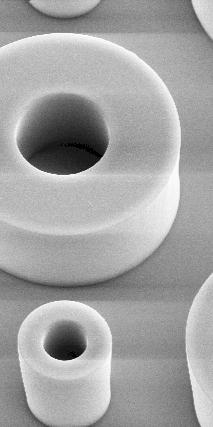
7 Innovation Positive E-Beam Resists 6200 (CSAR 62) Processing instructions Lift-off structures: Resist CSAR 62 is well suited to generate lift-off structures with a resolution of up to 10 nm. If the dose is increased by a factor of 1.5-2, narrow trenches with defined undercut can be fabricated with High layers for special applications: Films with a thickness of up to 800 nm can be produced With , and even 1.5-µm films are possible with experimental sample SX 6200/10. Undercut structures obtained with increased exposure dose : 100-nm trenches in 830-nm thick layer After vapour-deposition of metal and subsequent easy lift-off, metal structures remain CSAR 62 is also applied in various two-layer systems and can be used both as bottom and as top resist. 19-nm metal lines after lift-off process with as top resist for extreme lift-off applications Another field of application for CSAR 62 is the production of mask blanks which are coated with our resist and offered by our partners: CrAu test structures with a line width of 26 nm At a film thickness of 380 nm, 100-nm lines and spaces can be obtained on a chrome mask with The sensitivity is 12 µc/cm2 (20 kv, AR ). 7

. They immediately achieved a resolution of 50 nm which is an excellent value for masks.")

8 Positive E-Beam Resists 6200 (CSAR 62) Application examples for CSAR 62 Circuits for the 5 GHz range which are primarily needed for wireless Bluetooth or Wi-Fi technologies can in future be produced with CSAR 62. E-beam lithography is also required for the research on nanomaterials like graphene, for three-dimensional integrated circuits as well as for optical and quan-tum computers. The computing power or memory density is constantly increased in each of these technologies. Applications with the highest demands on computing power (supercomputers), e.g. in computational fluid dynamics or in space applications, thus also demand microchips with highest inte-gration density. CSAR 62 on mask blanks Experts at the HHI Berlin have already tested CSAR 62 on mask blanks ( Fig. 1). They immediately achieved a resolution of 50 nm which is an excellent value for masks. To date, 100 nm lines and above are used on masks. Currently test coatings of mask blanks with CSAR 62 are conducted, and samples will be offered by our partners to all customers in the near future. Fig. 2 Contrast curves 6200 and ZEP 520, 50kV, substrate: Si; ZEP 520, film thickness 220 nm, 60 s ZED N-50, contrast 6; 6200, film thickness 260 nm, 60 s AR , contrast 9 CSAR 62 for highest-resolution lithography In the work group for nanostructured materials, CSAR 62 is mainly used in highest-resolution lithography for the lift-off and as etching mask for dry chemical etching processes. The new resist offers several specific advantages. It achieves the high resolution of PMMA, but at a much lower dose, which is favourable for the following reason: CSAR 62 however counterbalances this effect due to its higher sensitivity, and in combination with the more favourable contrast curve can slight undercuts be achieved even in thin layers. This allows a uniform lift-off in the sub-100 nm range. As of December Fig. 1 CSAR 62 test structure on a mask blank with 50 nm lines and 50 nm trenches, pitch line & space nm Fabrication of plasmonic nanomaterials The work group for quantum detection has for already many years successfully promoted electron beam projects for nanostructuring. This group in particular emphasised the high process stability of CSAR 62 as compared to ZEP 520 ( Fig. 2). CSAR 62 is able to balance out small process fluc-tuations and still reliably provides the desired high resolution. The new Allresist product furthermore showed 1.5-fold higher contrast values than ZEP in comparative measurements. Fig. 3 Chrome structures with 20 nm lines after lift-off The goal in the lift-off of metal structures is however not always to go beyond the limits of resolution. Typical applications for example in the contacting of nanowires rather require dimensions in a range of nm, which can also be realised with other resists. The resolution reserve of CSAR 62 however allows for significantly improved structure accuracy and faster design with less iteration: Fig. 4 Typical structure for contacting nanowires. Large areas are mixed with small details

 was assessed.")
 restricts the minimum")
 illustrates the comparison of contrast values: ZEP 520 in the corresponding developer ZED-N50 and CSAR in developers AR 600-546 and 600-549.")
9 Positive E-Beam Resists 6200 (CSAR 62) Application examples for CSAR 62 During dry chemical etching, for example in the structuring of silicon nitride, CSAR combines the best of two worlds: It not only allows the use as a high resolution positive resist similar to PMMA, but also offers a stability which is comparable to novolacs. This facilitates the production of masks with sharp edges that provide the required etch stability without the otherwise frequently occurring disturbing faceted edges. In addition, a new variant of CSAR 62 with an extremely high layer thickness (1 µm) was assessed. The thick layer allows producing a strong undercut with only one layer, which is perfectly suitable for lift-off ( Fig. 5). The process is designed for larger surface areas in the micrometer range which should however clearly be defined since the pronounced undercut (as obvious from the figures) restricts the minimum distance between different structures. 2. Contrast: The diagram (Fig. 8) illustrates the comparison of contrast values: ZEP 520 in the corresponding developer ZED-N50 and CSAR in developers AR and While systems ZEP-ZED-N50 and CSAR-AR provide almost equally good contrast values, the contrast of CSAR in developer AR (which was specifically optimised for this purpose) is almost twice as high. This system is therefore ideally suited for high-resolution applications: Fig. 8 Contrast ZEP 520A, 200 nm, ZED N50 as well as , 200 nm, AR and AR Fig. 5 Particularly thick CSAR with pronounced undercut for extreme lift-off applications Comparison of CSAR 62 and ZEP 520A A leading company for electron-beam devices conducted a comparison of CSAR 62 and ZEP 520A. Using the current e-beam system SB 250, three comparative studies of CSAR 62 ( ) and ZEP 520A were carried out which focused on the parameters structural resolution, contrast and sensitivity in the respective native developers: 1. Structural resolution: The comparison of 90 nm lines of both resists ( Fig. 6 and 7) in the centre of a silicon wafer with a film thickness of 200 nm shows that both CSAR and ZEP are characterised by an excellent structural resolution (trench width of 91 nm, pitch 202 nm) and comparable broad process windows: Fig. 6 ZEP 520A, 200 nm, ZED N50, 50kV, 80 µc/cm² Fig , 200 nm, AR , 50 kv, 85 µc/cm² 3. Sensitivity (dose to clear): The diagram (Fig. 9) demonstrates a good range for the required dose of both resists. Again however, the CSAR resist-developer system with AR is twice as sensitive in comparison to the ZEP resist-developer system: Fig. 9 Sensitivity ZEP 520 A, 200 nm, ZED-N50 as well as , 200 nm, AR and All three studies come to the conclusion that ZEP 520A and CSAR 62 are both characterised by very good properties. CSAR 62 is thus an attractive alternative - with partly even more favourable application parameters. Advantages of CSAR 62 also arise from the variety of developers offered by Allresist, i.e. AR , and As of December
10 Thinner for AR resists AR , , , , thinner For adjusting the film thickness of photoresists and e-beam resists Characterisation - ultra-filtered, colourless, high-purity organic solvent mixtures - adjustment of resist film thickness by defined dilution: AR for photoresists, AR for e-beam resists - edge bead removal of coated substrates as well as cleaning of equipment - AR : removal of photoresist films tempered at up to 150 C and of non-tempered e-beam resist films Properties Parameter / AR Main component PGMEA chlorbenzene anisole methoxypropanol ethyl lactate Density at 20 C (g/cm 3 ) Refractive index at 20 C Water content max. (%) 0.1 Non-volatiles max. (%) Flash point ( C) Filtration (µm) 0.2 Suitable for dilution of 3000, 4000, AR photoresists 5000 Suitable for dilution of AR e-beam resists 6510, , 641, 661, , 642, 662, 672, , 649, 669, 679 Storage 6 month ( C) Application properties Dilution is performed as follows: I. placing of defined amount of resist, 2. addition of defined amount of thinner, 3. homogenisation by stirring (both liquids should be mixed quickly), and 4. fine filtration (0.2 µm). Information on dilution Higher dilutions of resists may cause gel formation of the polymers which leads to particle deposition in the resist film during the coating step. Diluted resists should therefore be subjected to ultra-filtration (0.2 µm) prior to use. In most cases it is more advantageous to adjust the desired film thickness by varying the spin speed or to utilise a pre-adjusted resist. Special adjustments of thickness values are possible on request for an additional charge. Formula for dilutions Example: Starting with a resist with 35 % solids content ( 3510), a solids content of 31 % is desired. Requested is the amount of thinner AR in g which has to be added to 100 g resist with 35 % solids content (mass m in g, solids content c /100). m thinner = m resist (c resist c desired) = g ( ) = 12.9 g thinner c desired 0.31 safer solvent If g resist (35 % solids content = 3510) are diluted with 12.9 g thinner in defined manner, g diluted resist (31 % solids content = 3540) will be obtained. With this dilution, the film thickness is reduced from 2.0 to 1.4 µm at a spin speed of 4000 rpm. 10
11 Characterisation - ultrapure, ultra-filtered (0.2 µm) solvent mixtures - storage at C for 6 month Properties Developer for AR E-Beam Resists AR , -51, , -548, -549, , -56 developer For the development of e-beam resists films AR resist / developer AR (new) AR AR AR Fields of application/conditions dip, puddle, spray development at C ± 1 C Main component(s) methoxypropanol / isopropyl alcohol Information on developer processing Innovation safer solvent butoxyethoxy ethanol methyl isobutyl ketone (MIBK) methyl isobutyl ketone (MIBK) Properties strong developer weaker developer Density at 20 C (g/cm3) Refractive index at 20 C Water content max. (%) Flash point ( C) min 5 min 3 min 3 min series - 3 min 1-3 min 1-3 min h - - AR resist / developer AR AR AR Fields of application/conditions dip, puddle, spray development at C ± 1 C Main component(s) amyl acetate diethyl ketone / diethyl malonate optimally suited diethyl malonate / anisole Properties weaker developer strong developer moderate developer Density at 20 C (g/cm3) Refractive index at 20 C Water content max. (%) Flash point ( C) min 1 min 1 min The choice of the developer strongly influences the development rate, the sensitivity and the profile of the resist structures. Coated and exposed substrates are treated with developers which are suitable for the respective process (puddle, spray, immersion bath) at a temperature of C kept as constant as possible. The required development time depends in each case on the resist film thickness. Films with a thickness of less than 0.2 µm can for example be completely developed after 30 s. The development process can be slowed down for AR , -55 and -56 by adding % of the stopper AR Weaker developers like AR and AR provide a higher resolution without dark erosion, while a significantly higher sensitivity with at the same time higher dark erosion can be obtained with developers AR and AR If CSAR 62 is processed with developer AR at a development temperature of about 0 C, even after 10 minutes no erosion is observed at the prolonged development time. Substrates have to be rinsed immediately after development for 30 seconds with stopper and are subsequently dried. suited 11
12 Stopper for AR Resists AR , stopper For the stopping of e-beam resist film development with solvents Characterisation - immediate interruption of the development process - ultrapure solvent mixtures for residue-free removal of remaining developer - AR for 617, er, AR for 6510 Properties I Parameter / AR Density at 20 C (g/cm³) Water content max. (%) Non-volatiles max. (%) Flash point ( C) Filtration (µm) 0.2 Storage up to 6 month ( C) Information on remover processing The addition of stopper for approximately 30 s after development interrupts the development process and leads to a rapid rinsing of residual developer. Due the processing regime however, constantly developer is transferred into the stopper bath. Already small amounts of the developer will affect the efficiency of the stopping process. It is thus highly recommended to constantly exchange the stopper or to use two stopper baths which are arranged consecutively. If % of stopper AR is added to developers AR , and , the development process is slowed down. If the stopper AR is used for developers , higher contrast values up to 10 are possible, while the sensitivity of the PMMA resists is at the same time decreased. Higher exposure doses and prolonged development times are thus required in this case. 12
13 600-70,,, , , remover For the stripping of tempered photoresist and e-beam resist films Characterisation - aqueous-alkaline solution (AR ) or organic solvents (all others) Remover recommendations after tempering: - photoresists up to 180 C: AR, - photoresists up to 200 C: AR, PMMAs up to 200 C: AR, - copolymers up to 210 C: AR, - CSAR 62 up to 200 C: AR, - novolac e-beam resists 150 C: AR, Remover recommendations Properties / Remover AR average time for removal at 1.5 μm Suitability for tempered photoresist films (21 C) Remover for AR Resists Properties new inexpensive, commonly used efficient allrounder * heated to 80 C universal, replacing the reprod. toxic, NEP: = AR , , * heated to 80 C universal, especially for thin films, but toxic for reproduction 120 C 15 s 10 s 25 s 20 s 30 s + heated to 50 C special: AR-BR 5400, 3100, 3500, C 20 s 15 s 3 min 25 s * 2 min 20 s * 2 min 60 s C 5 min 4 min 2 h 60 s * 2 h 50 s * 2 h 2 min C 30 min * 25 min * 30 min + Suitability for tempered e-beam resist films (21 C) inexpensive, commonly used efficient allrounder universal, replacing reprod. -toxic NEP: universal, but toxic for reproduction special: AR-N 7520, 7700 PMMA 150 C 25 s 20 s 20 min 10 s * 18 min 10 s * 15 min + PMMA 180 C 2 min 2 min 30 min 30 s * 28 min 30 s * 25 min + PMMA 200 C 3 min 3 min 42 min 50 s * 40 min 50 s * Copolymer C 10 s 5 s 60 s * 50 s * 20 min + CSAR C 30 s 60 s * 50 s * 10 min + CSAR C s 5 min * 4 min * min + Novolac-based C Novolac-based 150 C 5-60 s except s - 9 min except 7520, 7700 Innovation Parameter / AR s except s - 7 min except 7520, s * except 7520, s * except 7520, new , Main component acetone dioxolane DMG NEP TMAH Density at 20 C (g/cm3) Non-volatiles max. (%) Flash point ( C) Filtration (µm) 0.2 Storage up to 6 month ( C) optimally suitable suitable limited suitability unsuitable 5 s * except 7520, s - 3 min + 10 s * except 7520, s - 50 min + Processing instructions for removers Substrates coated with resist are exposed to the effect of the remover by immersion (puddle or dip). To reduce the dissolution time for tempered layers, removers AR , and may be heated to up to 80 C, remover AR to up to 50 C or megasound may be helpful in this case. It is recommended to rinse off the remover with DI water, clean remover or with a suitable thinner. A stripping of very hard-baked layers (> 220 C) with remover is hardly possible any more. In this case, oxidizing acids or oxygen plasma may be used for stripping. Further detailed remover specifications for a large variety of resists are listed on the following pages. 13
14 Remover for A Resists Remover recommendations < 20/ 60 s optimally suitable < 5/ 30 min suitable < 1-6 h limited suitability > 6 h unsuitable Product AR 3100 Example Example Example T Example 3540 T 3700 / 3800 Example Example 5350 AR-U 4000 Example 4040 C 500 Example Example 5910 AR-N 4200 Example 4240 Film thickness (µm) Tempering ( C) Recommend new , C 21 C 21 C 80 C 21 C 80 C 21 C 50 C < 20 s < 20 s < 20 s < 20 s < 20 s h < 20 s < 20 s < 60 s 180 (300-72) 6 h < 5 min < 60 s < 5 min < 60 s 1 h < 60 s 200 < 30 min < 30 min < 30 min < 20 s < 20 s < 20 s < 20 s < 5 min < 60 s 120 < 20 s < 20 s < 60 s < 60 s < 30 min < 5 min 150 < 60 s < 20 s < 5 min < 60 s < 5 min < 60 s < 30 min < 5 min h 1 h < 30 min 1 h < 30 min < 30 min h 1 h 2 h < 20 s < 20 s < 20 s < 20 s < 20 s 180 < 30 min < 5 min < 5 min < 20 s < 5 min < 20 s < 60 s < 20 s 200 < 1 h < 1 h 3 h < 30 min < 20 s < 20 s < 20 s < 20 s < 20 s h < 5 min < 60 s < 20 s < 5 min < 20 s < 30 min < 5 min 180 (300-72) < 30 min < 5 min < 5 min < 30 min h 1 h < 20 s < 20 s < 20 s < 20 s < 60 s 120 < 20 s < 20 s < 20 s < 20 s < 5 min < 20 s 150 < 60 s < 20 s < 60 s < 60 s < 5 min < 20 s 180 < 30 min < 30 min < 5 min < 60 s < 5 min < 60 s < 30 min < 60 s 200 < 30 min < 30 min 6 h < 30 min < 20 s < 20 s < 20 s < 20 s < 20 s 180 < 60 s < 60 s < 60 s < 60 s < 60 s h 1 h < 30 min < 20 s < 20 s < 20 s < 20 s < 20 s 120 < 20 s < 20 s < 20 s < 20 s < 60 s 150 (300-72) < 5 min < 5 min 3 h 180 < 30 min < 30 min < 5 min < 5 min < 1 h < 5 min < 1 h < 5 min < 5 min 190 (300-72) < 30 min < 30 min 1 h < 5 min 1 h < 5 min 4 h < 20 s < 20 s < 20 s < 20 s < 5 min 150 < 2 h < 30 min < 2 h < 30 min < 2 h < 5 min 180 (300-72) < 2 h < 20 s < 20 s < 20 s < 20 s < 20 s 180 < 20 s < 20 s < 60 s < 60 s < 5 min 200 < 1 h < 1 h < 1 h 14
15 Remover for AR Resists Remover recommendations < 20/ 60 s optimally suitable < 5/ 30 min suitable < 1-6 h limited suitability > 6 h unsuitable Product AR AR-N 4300 Example 4340 AR-N 4400 Example Example Example new Example Example AR-N 7500 Example AR-N 7520 new Example AR-N 7700 Example AR-N 7720 Example Film thickness (µm) Tempering ( C) Recommend new , C 21 C 21 C 80 C 21 C 80 C 21 C 50 C < 20 s < 20 s < 20 s < 20 s < 60 s (300-72) < 60 s < 30 min < 5 min < 60 s < 5 min 1 h 6 h < 60 s < 30 min h < 30 min < 30 min < 5 min < 30 min h 1 h 1 h < 30 min h 1 h < 20 s < 20 s < 5 min < 5 min < 5 min < 60 s < 60 s 120 < 5 min < 5 min 6 h < 60 s 5 h < 60 s 6 h < 30 min < 5 min < 5 min 1 h 1 h 2 h 180 < 30 min < 30 min 2 h 2 h h 4 h < 5 min < 5 min < 1 h < 60 s < 1 h < 60 s < 30 min 210 < 30 min < 5 min 6 h < 5 min 6 h < 5 min < 30 min < 20 s < 20 s < 30 min < 20 s < 30 min < 20 s < 30 min 180 (300-72) < 5 min < 5 min < 30 min < 60 s < 30 min < 60 s < 30 min 200 < 5 min < 5 min < 1 h < 60 s < 1 h < 60 s < 20 s < 30 min < 5 min < 30 min < 5 min < 30 min < 5 min 180 < 60 s < 30 min < 5 min < 30 min < 5 min < 1 h < 30 min 200 < 60 s < 30 min < 60 s < 30 min < 60 s < 30 min < 20 s < 20 s < 20 s < 20 s < 20 s < 20 s 120 < 20 s < 20 s < 20 s < 20 s < 20 s < 20 s 150 (300-72) < 5 min < 5 min 3 h 180 < 30 min < 30 min < 20 s < 20 s < 20 s < 20 s < 20 s h 4 h 3 h < 10 min < 20 s < 20 s < 20 s < 20 s < 20 s < 60 s 105 < 20 s < 20 s < 20 s < 20 s < 20 s < 5 min h 3 h < 30 min < 5 min h 4 h < 1 h < 1 h < 30 s < 1 h < 1 h < 60 s 120 < 1 h < 5 min h < 30 min < 60 s < 60 s < 20 s < 20 s < 20 s 150 < 5 min < 5 min 3 h < 5 min 2 h < 5 min < 60 s 180 (300-72) < 30 min < 30 min < 30 min < 30 min < 5 min h 1 h The average times required for removal as listed under properties are divided into time clusters (< 20 s, < 60 s ) for better orientation. In the column for remover recommendations, the first entry applies to low-baked and the second entry (or, if applicable, the third) to resist films baked at higher temperatures. The recommendation for remover AR is indicated in brackets, since this remover is highly effective, but also classified as toxic for reproduction and thus not prioritized by Allresist. As replacement, we recommend the equivalent removers AR and. 15
16 Adhesion Promoter for AR Resists AR and HMDS adhesion promoter For improving the adhesive strength of photo and e-beam resists Characterisation - improvement of the adhesive strength of photo and e-beam resist films - especially for surfaces with low adhesion properties, e.g. metal, SiO 2, GaAs - AR : spin coating of a diphenylsilanediol solution = improved adhesion properties and simple, cheaper alternative to HDMS - HMDS: evaporation of HMDS on the substrate surface (equipment required) Properties Parameter / AR HMDS Density at 20 C (g/cm3) Flash point ( C) Filtration (µm) Storage 6 month ( C) Processing information AR AR is applied by spin coating between 1000 and 6000 rpm. The film thickness can be adjusted by varying the spin speed to the optimum conditions of the respective process. Higher spin speeds and thus thinner films are preferable, e.g rpm with approx. 15 nm thickness. Too high concentrations (film thickness values) may reduce or neutralise the adhesion-promoting effect. It is recommended to perform the subsequent tempering on a hot plate for 2 min or in a convection oven for 25 min at 180 C. During tempering, a very uniform, extremely thin layer of adhesion promoter is generated on the substrate (approx. 15 nm). After cooling of the substrate, the resist can be applied as usual. An excess of adhesion promoter may be rinsed off with organic solvents like e.g. AR or AR. The optimised surface properties are maintained without restriction. Processing information HMDS Appropriate equipment is required for the processing of HMDS. The pre-treatment should be performed immediately prior to resist coating. Generally, hot plates with integrated HMDS-evaporation are used in the production. If this option is not available, the substrate is placed in a desiccator where HMDS evaporates at room temperature or at temperatures up to 160 C max. HMDS is under these conditions deposited as monomolecular layer (approx. 5 nm) on the substrate surface. The treated substrate can be coated with resist immediately after HMDS-deposition without subsequent tempering, or stored in a closed container for a couple of days. The storage stability may be limited due to an uptake of water from the atmosphere. Storage in open containers should thus be avoided. 16
17 17
18 Product Portfolio Photoresists We deliver our products within 1 week ex work, in-stock stock items are delivered immediately or on the desired date. Resists are available in package sizes of ¼, 0,5,1, 2,5, 6 x 1, 4 x 2,5 and corresponding process chemicals in package sizes of 1, 2,5, 5, 4 x 2,5, 4 x 5. Test samples/smallest quantities of 30 ml and 100 ml are possible.please request our price lists. Resist system Product Do/ µm 4000 rpm Type Characteristic Properties Resolution [µm] Thinner Application Contrast Exposure Deve- -loper Remover T 3700, AR-U 4000 C 500 AR-BR AR-N 2200 AR-N 4200 AR-N 4300 AR-N 4400 AR-N ,1220, , 3120, , 3220, , T, 3540 T 3740, , , dyed , 5480 [0.5-10] 1.0 ; 0.6 ; ; 10 ; ; ; ; ; ; 1.6 ; ; , 2220, , -25, -10, ; 0.5 [0.5-10] 1000 rpm: 50 ; 25 ; 10 ; rpm: 10 positive resist special application negative resist spray resist, var. applications high resolution, adhesion-enhanced thick resist with high dimen. accuracy up to 100 µm wide process range, high resolution wide process range, high res., developable in 0.26 n TMAH highest resolution, sub-µm, high contrast, 3840 dyed undercut structures (single layer lift-off) optinally pos. or neg., lift off protective coating, 40% KOH etch-stable bottom resist for 2L lift-off complicated patten. up to 5 % HF / BOE spray resist, var. applications highly sensitive, high resolution highest sensitivity, high resolution, CAR thick films up to 100, 50, 20, 10 µm, easy removal thick films up to 20 µm, lift-off MEMS 1 3 masks, lattices electroplating, MST All resist systems show optimal adhesion features with adhesion promoter AR which is applied prior to resist deposition. 0.5 ; 0.4 ; ; 3 ; 1.2 ICs 0.8 ; 0.7 ICs VLSIC structures ICs evaporation protective film lift-off (pos./neg.) 0.6 ; ; ; 2.0 ; ; ; ; 6.0 i-line, g-line, BB-UV ; ; ; 0.7; ; 3 ; ; 1.5 lift-off MEMS i-line, g-line, MEMS 1 3 BB-UV ICs ICs electroplating, MST, LIGA 5.0 ; 3.5 ; 2.0 ; ; 5 ; 4 ; 4 10 lift-off deep UV, i-line i-line, g-line X-ray, e-beam, i-line bis
19 Product Portfolio E-Beam Resists We deliver our products within 1 week ex work, in-stock stock items are delivered immediately or on the desired date. Resists are available in package sizes of ¼, 0,5,1, 2,5, 6 x 1, 4 x 2,5 and corresponding process chemicals in package sizes of 1, 2,5, 5, 4 x 2,5, 4 x 5. Test samples/smallest quantities of 30 ml and 100 ml are possible.please request our price lists. Resist system Product Do/ µm 4000 rpm Type Characteristic Properties Application Resolution [µm] * Contrast Exposure Thinner Developer Remover 617 copolymer PMMA/MA 33% methoxy propanole highest resolution, 2x more sensitiver than PMMA, lift off ICs, masks 10 / PMMA 50K, 200K, 600K, 950K chlorobenzene highest resolution, process stable, universally, simple processing ICs, masks 6 / PMMA 50K, 200K, 600K, 950K anisole highest resolution, process stable, universally, simple processing ICs, masks 6 / e-beam, deep UV PMMA 50K, 200K, 600K, 950K ethyl lactate positive highest resolution, process stable, universally, simple processing ICs, masks 6 / new CSAR ,.09, styrene acrylate 0.08 ; 0.4 ; 0.2 highest resolution, high sensitivity, plasma etching-resistant ICs, sensors, masks ,.18, PMMA 350 rpm: thick PMMA films up to 250 µm for MST, synchrotron micro components 1 µm (x-ray) 10 (x-ray) x-ray, e-beam AR-N 7500 AR-N 7520 new AR-N 7700 AR-N novolac , novolac ,.11, novolac , novolac , novolac ; ; 0.2; ; ; 1.4 negative mix&match, high resolution, plasma etchingresistant, also neg. mix&match, high resolution, plasma etchingresistant, pos./neg. mix&match, highest resolution, plasma etching resistent CAR, high resolution, high sensitivity, steep gradation CAR, high resolution, flat gradation for 3-dimens. struct. ICs, masks ICs, masks ICs, masks ICs, masks diffract. optics 40 / / / / 200 e-beam, deep UV, g-line, i-line e-beam, deep UV, i-line, e-beam, deep UV < All resist systems show optimal adhesion features with adhesion promoter AR which is applied prior to the resist. Note: If the stopper AR is used for developer , higher contrast values of up to 10 can be achieved. Resists 617, , 6200 require brief stopping in stopper AR after development. Resists of the 6500 series require brief stopping in stopper AR after development. * best value / industrial application As of December
20 Product Portfolio Experimental Samples We deliver our products within 1 week ex work, in-stock stock items are delivered immediately or on the desired date. Resists are available in package sizes of ¼, 0,5,1, 2,5, 6 x 1, 4 x 2,5 and corresponding process chemicals in package sizes of 1, 2,5, 5, 4 x 2,5, 4 x 5. Test samples/smallest quantities of 30 ml and 100 ml are possible.please request our price lists. Special product Do / µm 4000 rpm Type Characteristic properties / Application Resolution [µm] * Contrast Exposure Thinner Developer Remover Market-ready experimental samples X 3220/7 X 5800/7 X 5900/ positive temperature-/ plasma etching stable thick resist plasma etching positive resist for deep UV positive photoresist, alkalistable up to ph i-line. g- line, BB-UV deep UV, i-line i-line, g-line X AR-N 7700/ neg. highly sensitive, highestresolution CA negative e-beam resist e-beam, deep UV Special designs / Experimental samples SX 3500/6 SX 3740/ positive positive photoresist for holography (488 nm) positive photoresist, highly process-stable, high contrast i-line. g- line, BB-UV i-line. g- line, BB-UV SX AR-N 4340/7 1.4 neg. temperature-stable negative resist up to 300 C (2L-system) i-line, g-line SX C 5000/ protective coating for spray application, smooth surface SX C 5000/ protective coating 40% KOH- and 50% HF-resistant - 2 L: 10-2 L: 1-2 L: i-line / /1 SX C 5000/ polyimide photoresist, protective coating for 2 L-patterning - 2 L: 2-2 L: 1-2 L: i-line / SX 5000/ polyimide photoresist, structurable and temperature-stable SX C 5000/ conductive protective coating for PMMA-e-beam resists SX AR-N 7530 new SX AR-N 7730 new neg. white light e-beam resist like AR-N 7520 white light e-beam resist like AR-N i-line / DI water < 1.0 e-beam, deep UV All resist systems show optimal adhesion features with adhesion promoter AR which is applied prior to resist deposition. 20
21 Authors: Matthias and Brigitte Schirmer assisted by Dr. Christian Kaiser Layout: Ulrike Dorothea Schirmer Translation: S.K. Hemschemeier Copyright 2014 Allresist 21
")

22 Allresist GmbH Am Biotop Strausberg Germany Phone +49 (0) Fax +49 (0)
Major Fabrication Steps in MOS Process Flow
 Major Fabrication Steps in MOS Process Flow UV light Mask oxygen Silicon dioxide photoresist exposed photoresist oxide Silicon substrate Oxidation (Field oxide) Photoresist Coating Mask-Wafer Alignment
EG2605 Undergraduate Research Opportunities Program. Large Scale Nano Fabrication via Proton Lithography Using Metallic Stencils
 EG2605 Undergraduate Research Opportunities Program Large Scale Nano Fabrication via Proton Lithography Using Metallic Stencils Tan Chuan Fu 1, Jeroen Anton van Kan 2, Pattabiraman Santhana Raman 2, Yao
Atlas 46 novel negative tone photoresist which combines the good properties of the established SU-8 and CAR 44
 EIPBN, 30 th Mai 2018 Atlas 46 novel negative tone photoresist which combines the good properties of the established SU-8 and CAR 44 Dr. Christian Kaiser, Matthias Schirmer Allresist GmbH, Germany Outline
DOE Project: Resist Characterization
 DOE Project: Resist Characterization GOAL To achieve high resolution and adequate throughput, a photoresist must possess relatively high contrast and sensitivity to exposing radiation. The objective of
PHGN/CHEN/MLGN 435/535: Interdisciplinary Silicon Processing Laboratory. Simple Si solar Cell!
 Where were we? Simple Si solar Cell! Two Levels of Masks - photoresist, alignment Etch and oxidation to isolate thermal oxide, deposited oxide, wet etching, dry etching, isolation schemes Doping - diffusion/ion
Supporting Information 1. Experimental
 Supporting Information 1. Experimental The position markers were fabricated by electron-beam lithography. To improve the nanoparticle distribution when depositing aqueous Ag nanoparticles onto the window,
Part 5-1: Lithography
 Part 5-1: Lithography Yao-Joe Yang 1 Pattern Transfer (Patterning) Types of lithography systems: Optical X-ray electron beam writer (non-traditional, no masks) Two-dimensional pattern transfer: limited
MICROSTRUCTURING OF METALLIC LAYERS FOR SENSOR APPLICATIONS
 MICROSTRUCTURING OF METALLIC LAYERS FOR SENSOR APPLICATIONS Vladimír KOLAŘÍK, Stanislav KRÁTKÝ, Michal URBÁNEK, Milan MATĚJKA, Jana CHLUMSKÁ, Miroslav HORÁČEK, Institute of Scientific Instruments of the
Lecture 7. Lithography and Pattern Transfer. Reading: Chapter 7
 Lecture 7 Lithography and Pattern Transfer Reading: Chapter 7 Used for Pattern transfer into oxides, metals, semiconductors. 3 types of Photoresists (PR): Lithography and Photoresists 1.) Positive: PR
KMPR 1010 Process for Glass Wafers
 KMPR 1010 Process for Glass Wafers KMPR 1010 Steps Protocol Step System Condition Note Plasma Cleaning PVA Tepla Ion 10 5 mins Run OmniCoat Receipt Dehydration Any Heat Plate 150 C, 5 mins HMDS Coating
MeRck. AZ nlof technical datasheet. Negative Tone Photoresist for Single Layer Lift-Off APPLICATION TYPICAL PROCESS. SPIN CURVE (150MM Silicon)
") MeRck technical datasheet AZ nlof 5510 Negative Tone Photoresist for Single Layer Lift-Off APPLICATION AZ nlof 5510 i-line photoresist is engineered to simplify the historically complex image reversal
MeRck technical datasheet AZ nlof 5510 Negative Tone Photoresist for Single Layer Lift-Off APPLICATION AZ nlof 5510 i-line photoresist is engineered to simplify the historically complex image reversal
Semiconductor Manufacturing Technology. Semiconductor Manufacturing Technology. Photolithography: Resist Development and Advanced Lithography
 Semiconductor Manufacturing Technology Michael Quirk & Julian Serda October 2001 by Prentice Hall Chapter 15 Photolithography: Resist Development and Advanced Lithography Eight Basic Steps of Photolithography
MeRck. nlof 2000 Series. technical datasheet. Negative Tone Photoresists for Single Layer Lift-Off APPLICATION TYPICAL PROCESS
 MeRck technical datasheet AZ Negative Tone Photoresists for Single Layer Lift-Off APPLICATION AZ i-line photoresists are engineered to simplify the historically complex image reversal and multilayer lift-off
Section 2: Lithography. Jaeger Chapter 2 Litho Reader. The lithographic process
 Section 2: Lithography Jaeger Chapter 2 Litho Reader The lithographic process Photolithographic Process (a) (b) (c) (d) (e) (f) (g) Substrate covered with silicon dioxide barrier layer Positive photoresist
Section 2: Lithography. Jaeger Chapter 2 Litho Reader. EE143 Ali Javey Slide 5-1
 Section 2: Lithography Jaeger Chapter 2 Litho Reader EE143 Ali Javey Slide 5-1 The lithographic process EE143 Ali Javey Slide 5-2 Photolithographic Process (a) (b) (c) (d) (e) (f) (g) Substrate covered
Dr. Dirk Meyners Prof. Wagner. Wagner / Meyners Micro / Nanosystems Technology
 Micro/Nanosystems Technology Dr. Dirk Meyners Prof. Wagner 1 Outline - Lithography Overview - UV-Lithography - Resolution Enhancement Techniques - Electron Beam Lithography - Patterning with Focused Ion
+ Preferred material for tool O Acceptable material for tool X Unacceptable material for tool
 Contact Aligners (HTG, ABM, EV620) GCA 5X g-line Stepper GCA i-line Steppers (GCA 10X, AS200) Shipley 1800 Series (1805, 1813, 1818, 1827) + + X AZ nlof 2000 O X + AZ4903 + + X OiR 620-7i X X + OiR 897-12i
EE 143 Microfabrication Technology Fall 2014
 EE 143 Microfabrication Technology Fall 2014 Prof. Clark T.-C. Nguyen Dept. of Electrical Engineering & Computer Sciences University of California at Berkeley Berkeley, CA 94720 EE 143: Microfabrication
Section 2: Lithography. Jaeger Chapter 2. EE143 Ali Javey Slide 5-1
 Section 2: Lithography Jaeger Chapter 2 EE143 Ali Javey Slide 5-1 The lithographic process EE143 Ali Javey Slide 5-2 Photolithographic Process (a) (b) (c) (d) (e) (f) (g) Substrate covered with silicon
Outline. 1 Introduction. 2 Basic IC fabrication processes. 3 Fabrication techniques for MEMS. 4 Applications. 5 Mechanics issues on MEMS MDL NTHU
 Outline 1 Introduction 2 Basic IC fabrication processes 3 Fabrication techniques for MEMS 4 Applications 5 Mechanics issues on MEMS 2.2 Lithography Reading: Runyan Chap. 5, or 莊達人 Chap. 7, or Wolf and
Contrast Enhancement Materials CEM 365HR
 INTRODUCTION In 1989 Shin-Etsu Chemical acquired MicroSi, Inc. including their Contrast Enhancement Material (CEM) technology business*. A concentrated effort in the technology advancement of a CEM led
Lecture 13 Basic Photolithography
 Lecture 13 Basic Photolithography Chapter 12 Wolf and Tauber 1/64 Announcements Homework: Homework 3 is due today, please hand them in at the front. Will be returned one week from Thursday (16 th Nov).
Contrast Enhancement Materials CEM 365iS
 INTRODUCTION In 1989 Shin-Etsu Chemical acquired MicroSi, Inc. and the Contrast Enhancement Material (CEM) technology business from General Electric including a series of patents and technologies*. A concentrated
Chapter 3 Fabrication
 Chapter 3 Fabrication The total structure of MO pick-up contains four parts: 1. A sub-micro aperture underneath the SIL The sub-micro aperture is used to limit the final spot size from 300nm to 600nm for
FINDINGS. REU Student: Philip Garcia Graduate Student Mentor: Anabil Chaudhuri Faculty Mentor: Steven R. J. Brueck. Figure 1
 FINDINGS REU Student: Philip Garcia Graduate Student Mentor: Anabil Chaudhuri Faculty Mentor: Steven R. J. Brueck A. Results At the Center for High Tech Materials at the University of New Mexico, my work
Fabrication Techniques of Optical ICs
 Fabrication Techniques of Optical ICs Processing Techniques Lift off Process Etching Process Patterning Techniques Photo Lithography Electron Beam Lithography Photo Resist ( Microposit MP1300) Electron
Device Fabrication: Photolithography
 Device Fabrication: Photolithography 1 Objectives List the four components of the photoresist Describe the difference between +PR and PR Describe a photolithography process sequence List four alignment
Semiconductor Technology
 Semiconductor Technology from A to Z + - x 1 0 x Photolithographie www.halbleiter.org Contents Contents List of Figures III 1 Photolithographie 1 1.1 Exposure and resist coating..........................
Micro/Nanolithography
 Dale E. Ewbank dale.ewbank@rit.edu unl081413_microe.ppt 2013 Dale E. Ewbank page 1 OUTLINE Masks Optical Lithography Photoresist Sensitivity Processing Exposure Tools Advanced Processes page 2 MICROLITHOGRAPHY
Microlens formation using heavily dyed photoresist in a single step
 Microlens formation using heavily dyed photoresist in a single step Chris Cox, Curtis Planje, Nick Brakensiek, Zhimin Zhu, Jonathan Mayo Brewer Science, Inc., 2401 Brewer Drive, Rolla, MO 65401, USA ABSTRACT
POLYMER MICROSTRUCTURE WITH TILTED MICROPILLAR ARRAY AND METHOD OF FABRICATING THE SAME
 POLYMER MICROSTRUCTURE WITH TILTED MICROPILLAR ARRAY AND METHOD OF FABRICATING THE SAME Field of the Invention The present invention relates to a polymer microstructure. In particular, the present invention
Module 11: Photolithography. Lecture11: Photolithography - I
 Module 11: Photolithography Lecture11: Photolithography - I 1 11.0 Photolithography Fundamentals We will all agree that incredible progress is happening in the filed of electronics and computers. For example,
Integrated Focusing Photoresist Microlenses on AlGaAs Top-Emitting VCSELs
 Integrated Focusing Photoresist Microlenses on AlGaAs Top-Emitting VCSELs Andrea Kroner We present 85 nm wavelength top-emitting vertical-cavity surface-emitting lasers (VCSELs) with integrated photoresist
Photolithography I ( Part 1 )
") 1 Photolithography I ( Part 1 ) Chapter 13 : Semiconductor Manufacturing Technology by M. Quirk & J. Serda Bjørn-Ove Fimland, Department of Electronics and Telecommunication, Norwegian University of Science
1 Photolithography I ( Part 1 ) Chapter 13 : Semiconductor Manufacturing Technology by M. Quirk & J. Serda Bjørn-Ove Fimland, Department of Electronics and Telecommunication, Norwegian University of Science
Low-power carbon nanotube-based integrated circuits that can be transferred to biological surfaces
 SUPPLEMENTARY INFORMATION Articles https://doi.org/10.1038/s41928-018-0056-6 In the format provided by the authors and unedited. Low-power carbon nanotube-based integrated circuits that can be transferred
Microlithography. Dale E. Ewbank ul ppt. Microlithography Dale E. Ewbank page 1
 Dale E. Ewbank dale.ewbank@rit.edu ul012014.ppt 2014 Dale E. Ewbank page 1 OUTLINE Masks Optical Lithography Photoresist Sensitivity Processing Exposure Tools Advanced Processes page 2 MICROLITHOGRAPHY
EE143 Fall 2016 Microfabrication Technologies. Lecture 3: Lithography Reading: Jaeger, Chap. 2
 EE143 Fall 2016 Microfabrication Technologies Lecture 3: Lithography Reading: Jaeger, Chap. 2 Prof. Ming C. Wu wu@eecs.berkeley.edu 511 Sutardja Dai Hall (SDH) 1-1 The lithographic process 1-2 1 Photolithographic
This writeup is adapted from Fall 2002, final project report for by Robert Winsor.
 Optical Waveguides in Andreas G. Andreou This writeup is adapted from Fall 2002, final project report for 520.773 by Robert Winsor. September, 2003 ABSTRACT This lab course is intended to give students
Supplementary Figure 1: Optical Properties of V-shaped Gold Nanoantennas a) Illustration of the possible plasmonic modes.
 Illustration of the possible plasmonic modes.") Supplementary Figure 1: Optical Properties of V-shaped Gold Nanoantennas a) Illustration of the possible plasmonic modes. S- symmetric, AS antisymmetric. b) Calculated linear scattering spectra of individual
Supplementary Figure 1: Optical Properties of V-shaped Gold Nanoantennas a) Illustration of the possible plasmonic modes. S- symmetric, AS antisymmetric. b) Calculated linear scattering spectra of individual
Design Rules for Silicon Photonics Prototyping
 Design Rules for licon Photonics Prototyping Version 1 (released February 2008) Introduction IME s Photonics Prototyping Service offers 248nm lithography based fabrication technology for passive licon-on-insulator
Plan Optik AG. Plan Optik AG PRODUCT CATALOGUE
 Plan Optik AG Plan Optik AG PRODUCT CATALOGUE 2 In order to service the high demand of wafers more quickly, Plan Optik provides off the shelf products in sizes from 2 up to 300mm diameter. Therefore Plan
Supplementary Materials for
 www.sciencemag.org/cgi/content/full/science.1234855/dc1 Supplementary Materials for Taxel-Addressable Matrix of Vertical-Nanowire Piezotronic Transistors for Active/Adaptive Tactile Imaging Wenzhuo Wu,
William Reiniach 5th Year Microelectronic Engineering Student Rochester Institute of Technology
 DEVELOPMENT OF A PHOTOSENSITIVE POLYIMIDE PROCESS William Reiniach 5th Year Microelectronic Engineering Student Rochester Institute of Technology 1~BS TRACT A six step lithographic process has been developed
Optimization of PMMA 950KA4 resist patterns using Electron Beam Lithography
 CeNSE restricted NNFC-TN 2017/001 Technical Note CENSE-NNFC-2017/001 Issued: 03/2017 Optimization of PMMA 950KA4 resist patterns using Electron Beam Lithography Sreedhar Babu, Anita CeNSE, NNFC, Indian
i- Line Photoresist Development: Replacement Evaluation of OiR
 i- Line Photoresist Development: Replacement Evaluation of OiR 906-12 Nishtha Bhatia High School Intern 31 July 2014 The Marvell Nanofabrication Laboratory s current i-line photoresist, OiR 897-10i, has
MICROBUMP CREATION SYSTEM FOR ADVANCED PACKAGING APPLICATIONS
 MICROBUMP CREATION SYSTEM FOR ADVANCED PACKAGING APPLICATIONS Andrew Ahr, EKC Technology, & Chester E. Balut, DuPont Electronic Technologies Alan Huffman, RTI International Abstract Today, the electronics
Module - 2 Lecture - 13 Lithography I
 Nano Structured Materials-Synthesis, Properties, Self Assembly and Applications Prof. Ashok. K.Ganguli Department of Chemistry Indian Institute of Technology, Delhi Module - 2 Lecture - 13 Lithography
Module 11: Photolithography. Lecture 14: Photolithography 4 (Continued)
") Module 11: Photolithography Lecture 14: Photolithography 4 (Continued) 1 In the previous lecture, we have discussed the utility of the three printing modes, and their relative advantages and disadvantages.
Module 11: Photolithography Lecture 14: Photolithography 4 (Continued) 1 In the previous lecture, we have discussed the utility of the three printing modes, and their relative advantages and disadvantages.
Fabrication Methodology of microlenses for stereoscopic imagers using standard CMOS process. R. P. Rocha, J. P. Carmo, and J. H.
 Fabrication Methodology of microlenses for stereoscopic imagers using standard CMOS process R. P. Rocha, J. P. Carmo, and J. H. Correia Department of Industrial Electronics, University of Minho, Campus
Hermetic Packaging Solutions using Borosilicate Glass Thin Films. Lithoglas Hermetic Packaging Solutions using Borosilicate Glass Thin Films
 Hermetic Packaging Solutions using Borosilicate Glass Thin Films 1 Company Profile Company founded in 2006 ISO 9001:2008 qualified since 2011 Headquarters and Production in Dresden, Germany Production
Transparent p-type SnO Nanowires with Unprecedented Hole Mobility among Oxide Semiconductors
 Supplementary Information Transparent p-type SnO Nanowires with Unprecedented Hole Mobility among Oxide Semiconductors J. A. Caraveo-Frescas and H. N. Alshareef* Materials Science and Engineering, King
PROFILE CONTROL OF A BOROSILICATE-GLASS GROOVE FORMED BY DEEP REACTIVE ION ETCHING. Teruhisa Akashi and Yasuhiro Yoshimura
 Stresa, Italy, 25-27 April 2007 PROFILE CONTROL OF A BOROSILICATE-GLASS GROOVE FORMED BY DEEP REACTIVE ION ETCHING Teruhisa Akashi and Yasuhiro Yoshimura Mechanical Engineering Research Laboratory (MERL),
32nm High-K/Metal Gate Version Including 2nd Generation Intel Core processor family
 From Sand to Silicon Making of a Chip Illustrations 32nm High-K/Metal Gate Version Including 2nd Generation Intel Core processor family April 2011 1 The illustrations on the following foils are low resolution
Marabu. Glass Ink GL. Field of Application. Characteristics
 Screen Printing Ink for glass, ceramics, metals, aluminium, chrome-plated parts, coated substrates, and thermosetting plastics Satin-gloss finish, semi-opaque, fast drying 2-component-ink-system, dishwasherproof
Photolithography Technology and Application
 Photolithography Technology and Application Jeff Tsai Director, Graduate Institute of Electro-Optical Engineering Tatung University Art or Science? Lind width = 100 to 5 micron meter!! Resolution = ~ 3
Monolithically integrated InGaAs nanowires on 3D. structured silicon-on-insulator as a new platform for. full optical links
 Monolithically integrated InGaAs nanowires on 3D structured silicon-on-insulator as a new platform for full optical links Hyunseok Kim 1, Alan C. Farrell 1, Pradeep Senanayake 1, Wook-Jae Lee 1,* & Diana.
KODALITH Ortho Films 2556,6556, Type 3
 TECHNICAL INFORMATION INSTRUCTION SHEET KODALITH Ortho Films 2556,6556, Type 3 Features/Customer Product Specification Extremely high contrast, orthochromatic film designed primarily for making line and
Exhibit 2 Declaration of Dr. Chris Mack
 STC.UNM v. Intel Corporation Doc. 113 Att. 5 Exhibit 2 Declaration of Dr. Chris Mack Dockets.Justia.com UNITED STATES DISTRICT COURT DISTRICT OF NEW MEXICO STC.UNM, Plaintiff, v. INTEL CORPORATION Civil
2.1 BASIC THEORY: INTERFERENCE OF TWO BEAMS
 2 LASER INTERFERENCE LITHOGRAPHY (LIL) 9 2 LASER INTERFERENCE LITHOGRAPHY (LIL) Laser interference lithography [3~22] (LIL) is a method to produce periodic structures using two interfering highly-coherent
College of Engineering Department of Electrical Engineering and Computer Sciences University of California, Berkeley
 College of Engineering Department of Electrical Engineering and Below are your weekly quizzes. You should print out a copy of the quiz and complete it before your lab section. Bring in the completed quiz
THE USE OF A CONTRAST ENHANCEMENT LAYER TO EXTEND THE PRACTICAL RESOLUTION LIMITS OF OPTICAL LITHOGRAPHIC SYSTEMS
 THE USE OF A CONTRAST ENHANCEMENT LAYER TO EXTEND THE PRACTICAL RESOLUTION LIMITS OF OPTICAL LITHOGRAPHIC SYSTEMS Daniel R. Sutton 5th Year Microelectronic Engineering Student Rochester Institute of Technology
Nanofluidic Diodes based on Nanotube Heterojunctions
 Supporting Information Nanofluidic Diodes based on Nanotube Heterojunctions Ruoxue Yan, Wenjie Liang, Rong Fan, Peidong Yang 1 Department of Chemistry, University of California, Berkeley, CA 94720, USA
CMOS Digital Integrated Circuits Lec 2 Fabrication of MOSFETs
 CMOS Digital Integrated Circuits Lec 2 Fabrication of MOSFETs 1 CMOS Digital Integrated Circuits 3 rd Edition Categories of Materials Materials can be categorized into three main groups regarding their
PCB Fabrication Processes Brief Introduction
 PCB Fabrication Processes Brief Introduction AGS-Electronics, Ph: +1-505-550-6501 or +1-505-565-5102, Fx: +1-505-814-5778, Em: sales@ags-electronics.com, Web: http://www.ags-electronics.com Contents PCB
Chapter 6. Photolithography
 Chapter 6 Photolithography 2006/4/10 1 Objectives List the four components of the photoresist Describe the difference between +PR and PR Describe a photolithography process sequence List four alignment
CHAPTER 2 Principle and Design
 CHAPTER 2 Principle and Design The binary and gray-scale microlens will be designed and fabricated. Silicon nitride and photoresist will be taken as the material of the microlens in this thesis. The design
Project Staff: Feng Zhang, Prof. Jianfeng Dai (Lanzhou Univ. of Tech.), Prof. Todd Hasting (Univ. Kentucky), Prof. Henry I. Smith
, Prof. Todd Hasting (Univ. Kentucky), Prof. Henry I. Smith") 3. Spatial-Phase-Locked Electron-Beam Lithography Sponsors: No external sponsor Project Staff: Feng Zhang, Prof. Jianfeng Dai (Lanzhou Univ. of Tech.), Prof. Todd Hasting (Univ. Kentucky), Prof. Henry
3. Spatial-Phase-Locked Electron-Beam Lithography Sponsors: No external sponsor Project Staff: Feng Zhang, Prof. Jianfeng Dai (Lanzhou Univ. of Tech.), Prof. Todd Hasting (Univ. Kentucky), Prof. Henry
AEROSOL JET PRINTING SYSTEM FOR HIGH SPEED, NON-CONTACT FRONT SIDE METALLIZATION OF SILICON SOLAR CELLS
 AEROSOL JET PRINTING SYSTEM FOR HIGH SPEED, NON-CONTACT FRONT SIDE METALLIZATION OF SILICON SOLAR CELLS Bruce H. King and Stephen M. Barnes Optomec, Inc. 3911 Singer NE, Albuquerque, NM 87109, US Phone
plasmonic nanoblock pair
 Nanostructured potential of optical trapping using a plasmonic nanoblock pair Yoshito Tanaka, Shogo Kaneda and Keiji Sasaki* Research Institute for Electronic Science, Hokkaido University, Sapporo 1-2,
Soft Electronics Enabled Ergonomic Human-Computer Interaction for Swallowing Training
 Supplementary Information Soft Electronics Enabled Ergonomic Human-Computer Interaction for Swallowing Training Yongkuk Lee 1,+, Benjamin Nicholls 2,+, Dong Sup Lee 1, Yanfei Chen 3, Youngjae Chun 3,4,
Fabrication of micro structures on curve surface by X-ray lithography
 Fabrication of micro structures on curve surface by X-ray lithography Yigui Li 1, Susumu Sugiyama 2 Abstract We demonstrate experimentally the x-ray lithography techniques to fabricate micro structures
Lithography. 3 rd. lecture: introduction. Prof. Yosi Shacham-Diamand. Fall 2004
 Lithography 3 rd lecture: introduction Prof. Yosi Shacham-Diamand Fall 2004 1 List of content Fundamental principles Characteristics parameters Exposure systems 2 Fundamental principles Aerial Image Exposure
Supplementary Figure 1 Reflective and refractive behaviors of light with normal
 Supplementary Figures Supplementary Figure 1 Reflective and refractive behaviors of light with normal incidence in a three layer system. E 1 and E r are the complex amplitudes of the incident wave and
On-chip 3D air core micro-inductor for high-frequency applications using deformation of sacrificial polymer
 header for SPIE use On-chip 3D air core micro-inductor for high-frequency applications using deformation of sacrificial polymer Nimit Chomnawang and Jeong-Bong Lee Department of Electrical and Computer
T in sec, I in W/cm 2, E in J/cm 2
 Exposures from Mask Aligner into Resist Mask aligner images created by shadowing from mask into resist Soft contact and Proximity good for 3 micron structures Vacuum Hard Contact: no shadow effects at
Micro-sensors - what happens when you make "classical" devices "small": MEMS devices and integrated bolometric IR detectors
 Micro-sensors - what happens when you make "classical" devices "small": MEMS devices and integrated bolometric IR detectors Dean P. Neikirk 1 MURI bio-ir sensors kick-off 6/16/98 Where are the targets
3.Photolithography and resist systems
 3.Photolithography and resist systems Exposure Mercury arc lamp Shadow printing projection printing Photomask Substrates Resist systems DNQ-Novolak-based Epoxy-based Polyimide based 1 Exposure Mercury
DIY fabrication of microstructures by projection photolithography
 DIY fabrication of microstructures by projection photolithography Andrew Zonenberg Rensselaer Polytechnic Institute 110 8th Street Troy, New York U.S.A. 12180 zonena@cs.rpi.edu April 20, 2011 Abstract
Chapter 6 Photolithography
 Chapter 6 Photolithography Hong Xiao, Ph. D. hxiao89@hotmail.com www2.austin.cc.tx.us/hongxiao/book.htm Hong Xiao, Ph. D. www2.austin.cc.tx.us/hongxiao/book.htm 1 Objectives List the four components of
Infinitely Precise. micrometal. excellence in etching
 Infinitely Precise micrometal excellence in etching A High-Tech Profile Superfine structures and ultra-tight tolerances: precision is our business You give us the specs, and we etch to ultra-tight tolerances.
Optical Bus for Intra and Inter-chip Optical Interconnects
 Optical Bus for Intra and Inter-chip Optical Interconnects Xiaolong Wang Omega Optics Inc., Austin, TX Ray T. Chen University of Texas at Austin, Austin, TX Outline Perspective of Optical Backplane Bus
Development of Nanoimprint Mold Using JBX-9300FS
 Development of Nanoimprint Mold Using JBX-9300FS Morihisa Hoga, Mikio Ishikawa, Naoko Kuwahara Tadahiko Takikawa and Shiho Sasaki Dai Nippon Printing Co., Ltd Research & Development Center Electronic Device
Sensors & Transducers Published by IFSA Publishing, S. L., 2016
 Sensors & Transducers Published by IFSA Publishing, S. L., 2016 http://www.sensorsportal.com Development of a Novel High Reliable Si-Based Trace Humidity Sensor Array for Aerospace and Process Industry
Cold curing adhesive K-X280
 Instructions for use English Cold curing adhesive K-X280 A4048-1.0 en English 1 Safety instructions... 3 2 General information... 3 2.1 Scope of delivery for K-X280... 3 2.2 Accessories required for installation...
T in sec, I in W/cm 2, E in J/cm 2
 Exposures from Mask Aligner into Resist Mask aligner images created by shadowing from mask into resist Soft contact and Proximity good for 3 micron structures Vacuum Hard Contact: no shadow effects at
Supplementary Information
 Supplementary Information Wireless thin film transistor based on micro magnetic induction coupling antenna Byoung Ok Jun 1, Gwang Jun Lee 1, Jong Gu Kang 1,2, Seung Uk Kim 1, Ji Woong Choi 1, Seung Nam
Sub-50 nm period patterns with EUV interference lithography
 Microelectronic Engineering 67 68 (2003) 56 62 www.elsevier.com/ locate/ mee Sub-50 nm period patterns with EUV interference lithography * a, a a b b b H.H. Solak, C. David, J. Gobrecht, V. Golovkina,
COMPARISON OF ULTIMATE RESOLUTION ACHIEVED BY E-BEAM WRITERS WITH SHAPED BEAM AND WITH GAUSSIAN BEAM
 COMPARISON OF ULTIMATE RESOLUTION ACHIEVED BY E-BEAM WRITERS WITH SHAPED BEAM AND WITH GAUSSIAN BEAM Stanislav KRÁTKÝ a, Vladimír KOLAŘÍK a, Milan MATĚJKA a, Michal URBÁNEK a, Miroslav HORÁČEK a, Jana
Coating of Si Nanowire Array by Flexible Polymer
 , pp.422-426 http://dx.doi.org/10.14257/astl.2016.139.84 Coating of Si Nanowire Array by Flexible Polymer Hee- Jo An 1, Seung-jin Lee 2, Taek-soo Ji 3* 1,2.3 Department of Electronics and Computer Engineering,
End-of-line Standard Substrates For the Characterization of organic
 FRAUNHOFER INSTITUTe FoR Photonic Microsystems IPMS End-of-line Standard Substrates For the Characterization of organic semiconductor Materials Over the last few years, organic electronics have become
Nano-structured superconducting single-photon detector
 Nano-structured superconducting single-photon detector G. Gol'tsman *a, A. Korneev a,v. Izbenko a, K. Smirnov a, P. Kouminov a, B. Voronov a, A. Verevkin b, J. Zhang b, A. Pearlman b, W. Slysz b, and R.
Transistor was first invented by William.B.Shockley, Walter Brattain and John Bardeen of Bell Labratories. In 1961, first IC was introduced.
 Unit 1 Basic MOS Technology Transistor was first invented by William.B.Shockley, Walter Brattain and John Bardeen of Bell Labratories. In 1961, first IC was introduced. Levels of Integration:- i) SSI:-
FABRICATION OF CMOS INTEGRATED CIRCUITS. Dr. Mohammed M. Farag
 FABRICATION OF CMOS INTEGRATED CIRCUITS Dr. Mohammed M. Farag Outline Overview of CMOS Fabrication Processes The CMOS Fabrication Process Flow Design Rules Reference: Uyemura, John P. "Introduction to
Mobile Electrostatic Carrier (MEC) evaluation for a GaAs wafer backside manufacturing process
 evaluation for a GaAs wafer backside manufacturing process") Mobile Electrostatic Carrier (MEC) evaluation for a GaAs wafer backside manufacturing process H.Stieglauer 1, J.Nösser 1, A.Miller 1, M.Lanz 1, D.Öttlin 1, G.Jonsson 1, D.Behammer 1, C.Landesberger 2,
Mobile Electrostatic Carrier (MEC) evaluation for a GaAs wafer backside manufacturing process H.Stieglauer 1, J.Nösser 1, A.Miller 1, M.Lanz 1, D.Öttlin 1, G.Jonsson 1, D.Behammer 1, C.Landesberger 2,
Technical Product Information
 O.D. Thermochromic Function: Irreversible Product Name: Kromagen Black K60-NH Last Revision: 11/02/2015 Technical Product Information Kromagen Black K60-NH can be supplied as a Concentrate, Water Based
Photonic device package design, assembly and encapsulation.
 Photonic device package design, assembly and encapsulation. Abstract. A.Bos, E. Boschman Advanced Packaging Center. Duiven, The Netherlands Photonic devices like Optical transceivers, Solar cells, LED
Feature-level Compensation & Control
 Feature-level Compensation & Control 2 Sensors and Control Nathan Cheung, Kameshwar Poolla, Costas Spanos Workshop 11/19/2003 3 Metrology, Control, and Integration Nathan Cheung, UCB SOI Wafers Multi wavelength
From Sand to Silicon Making of a Chip Illustrations May 2009
 From Sand to Silicon Making of a Chip Illustrations May 2009 1 The illustrations on the following foils are low resolution images that visually support the explanations of the individual steps. For publishing
Forming a vertical interconnect structure using dry film processing for Fan Out Wafer Level Packaging
 2017 IEEE 67th Electronic Components and Technology Conference Forming a vertical interconnect structure using dry film processing for Fan Out Wafer Level Packaging Yew Wing Leong, Hsiang Yao Hsiao, Soon
Suggested Specification for Preparing Hot-Dip Galvanized Steel Surfaces for Painting Revised February 2002
 Suggested Specification for Preparing Hot-Dip Galvanized Steel Surfaces for Painting Revised February 2002 This suggested specification is provided as a guide to preparing a quality document calling for