Low power SERDES transceiver for supply-induced jitter sensitivity methodology analysis
|
|
|
- Molly Wilkerson
- 5 years ago
- Views:
Transcription

1 Low power SERDES transceiver for supply-induced jitter sensitivity methodology analysis Micro Chang htc Jan 9, 2019 X 1
2 Agenda Jitter-aware target impedance of power delivery network approach Design challenge for Low power Transmitter CLK path : DCC & CLK tree buffer and its side effect Data path : Pre-driver & CML IO Design challenge for Receiver Recover very loss signal. Needs re-driver. Design challenge for PLL Ring VCO Solution to Design Challenge Solution to CLK path : Active & passive method Solution to Data path: Current modulation skill Solution to recover very loss signal for receiver : Multi-stage CTLE&VGA cascade design Summary X 2
3 Jitter-aware target impedance of power delivery network approach Introduction : To complete the PDN analysis, it is necessary to determine the target impedance of the overall power network. However conventional target impedance only shows on-chip supply noise value information. Conventional target impedance does not show any jitterrelated information. With jitter sensitivity extraction of IO circuit, it is to enable accurate jitter-aware target impedance calculation X 3
4 Jitter-accumulation of Low Power Transmitter Data & CLK path approach PLL Core domain Core domain Core domain IO domain Parallel to serial 2 to 1 Pre-driver CML IO Jitter accumulation path PLL Duty cycle corrector CLK IO & Core domain CLK Tree CLK Core domain General SERDES transmitter architecture is serial-to-parallel converter and is sensitivity to the supply noise. The serdes transmitter has many power domains which have different influences in the jitter-sensitivity contribution. The jitter sensitivity is dependent of each block silicon characterization and combined with Data/CLK path. X 4
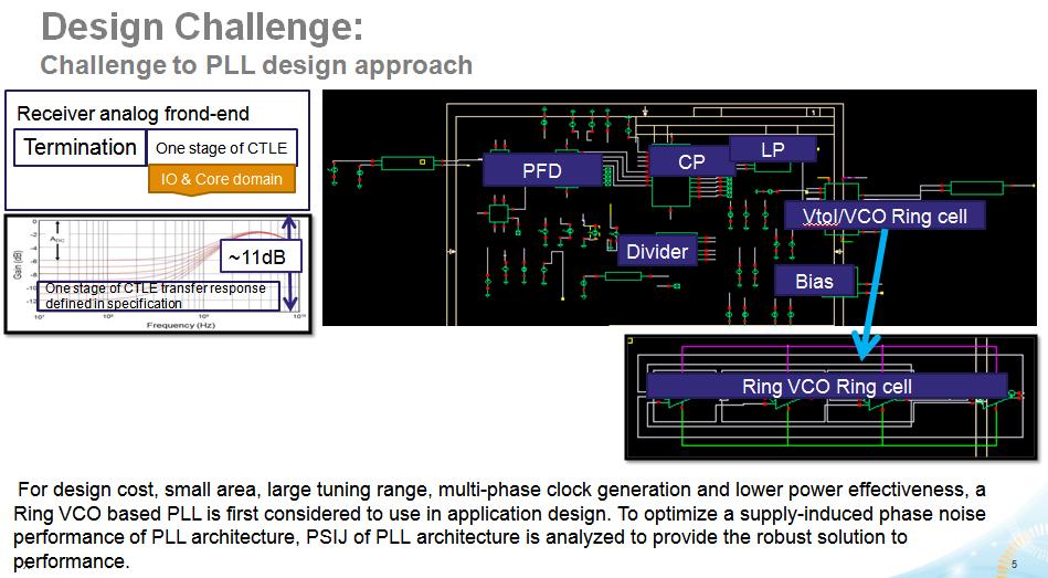
5 X 5


6 Challenge to Jitter-accumulation of Low Power Transmitter CLK path approach W/o DCC W/ DCC Jitter accumulation CLK path Jitter accumulation path Duty cycle % = 33%~67% Duty cycle % = 49%~51% Duty cycle corrector function and its side effect: Duty cycle corrector is commonly used to adjust the duty cycle of clock signals from PLL, to improve the signal quality of the clock signal and to ensure a ~50% duty cycle that maintain the high speed signal performance. However its supply-induced jitter sensitivity is increased, and the performance is affected. X 6
 X axis: Frequency Need a lot of resource of on-chip decap, Package and PCB BOM cost")

7 Challenge to Jitter-accumulation of Low Power Transmitter CLK path approach Supply-induced jitter sensitivity Plot Jitter-aware target impedance Plot CLK core Jitter-aware target impedance CLK core 2~3 order Fail Region CLK IO Pass Region Y axis: Degree/V X axis: Frequency Y axis: Impedance(ohm) X axis: Frequency Need a lot of resource of on-chip decap, Package and PCB BOM cost to meet the PDN target impedance requirement. Reach to the goal with difficulty CLK path supply induced jitter analysis : Merge Core power and CLK core power in Die-package bump region that causes the very strict requirement of target impedance because core power supply many blocks which is power hungry such as clock data recovery/receiver AFE/Transmitter logics and pre-drivers. X 7


8 Challenge to Jitter-accumulation of Low Power Transmitter Data approach Jitter accumulation Data path Core-PSIJ ~3 order Jitter accumulation path IO-PSIJ Y axis: Degree/V X axis: Frequency Need a lot of resource of on-chip decap, Package and PCB BOM cost to meet the Core power target impedance requirement. Reach to the goal with difficulty Introduction : For optimizing this jitter performance induced by supply noise, characterizing the jitter distribution between different power domains is the key to resource allocation of PDN design. The simulation shows that if an internal data path is consist of voltage mode pre-driver, it is sensitive to core power supply noise. X 8
9 Power supply & common mode noise induced jitter of Receiver AFE approach PSIJ(Core) Signal Common mode noise induced jitter CMIJ Power supply noise induced jitter PSIJ PSIJ (IO) CMIJ Y axis: Degree/V X axis: Frequency Reach to the PDN Z goal with No difficulty Due to the complexity of CM/Power supply noise generated from non-linear power supply noise/nonsymmetry Packaging/PCB trace, the effect of common mode noise is analyzed independently to investigate the CM noise induced jitter inside receiver. X 9

10 Challenge to Receiver AFE recover ability approach Receiver analog frond-end Termination One stage of CTLE IO & Core domain ~11dB One stage of CTLE transfer response defined in specification If channel= ~27dB??? Eye closure Need re-driver/re-timer!!! The received signal, however, suffers from seriously inter-symbol interference (ISI) due to channel imperfections making the signal integrity face big challenges. Re-driver/Re-timer requirement is always strong demand but brings more power consumption, cost and form factor. X 10
11 X 11
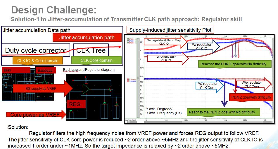
12 Solution-2 to Jitter-accumulation of Transmitter CLK path approach: Separated coupling layout skill similar to on-chip regulator behavior Jitter accumulation Data path Duty cycle corrector Jitter accumulation path CLK Tree Jitter-aware target impedance Plot Target impedance Specification requirement ~2 order improvement CLK IO & Core domain CLK Core domain Y axis: Impedance(ohm) X axis: Frequency Reach to the PDN Z goal with No difficulty REG on board Power PCB path PKG path1 PKG path2 Core power Transmitter CLK Core power Solution : Separate Core power and CLK core power in Die-package and merged together under board-level BGA region. Specification requirement is relaxed by ~2 order and likely to meet. Separated layout skill is similar to on-chip regulator behavior and without any additional power consumption. Voltage transfer curve from core power to CLK core power at transmitter with PKG/PCB Follow core power at low frequency, Filter noise ~-18dB isolation at high frequency ~18dB isolation X 12


13 Solution to Jitter-accumulation of Transmitter Data approach Jitter-aware Target PDN Z based on Current modulation 2to1 Pre-driver chain CML IO Jitter-aware Target PDN Z based on Non-Current modulation Dummy path Dummy Pre-driver chain Dummy CML IO Current profile modulation CLK tree Main path 1~2 order improvement PDN goal Dummy path Non-Current profile modulation Y axis: Impedance(ohm) X axis: Frequency Current profile modulation skill is applied in analog skill to analyze the improvement of target impedance of Core power domain PDN. Specification requirement is relaxed by 1~2 order. X 13
 ~27dB Supply-induced jitter sensitivity Plot PSIJ(Core) PSIJ (IO) CMIJ Common mode noise induced jitter CMIJ Power supply noise induced jitter PSIJ Good cascade")

14 Solution to recover very loss signal for receiver approach: Multi-stage CTLE&VGA cascade design Receiver Analog frond-end Signal path Customized Cascade CTLE+VGA Customized Cascade CTLE+VGA transfer response Bad cascade design PSIJ(Core) ~27dB Supply-induced jitter sensitivity Plot PSIJ(Core) PSIJ (IO) CMIJ Common mode noise induced jitter CMIJ Power supply noise induced jitter PSIJ Good cascade design Jitter Sensitivity slightly increases. Reach to the PDN goal with No difficulty PASS 27dB channel with RX AFE enable only Supply-induced jitter sensitivity Plot Solution : Customized AFE Receiver overcomes the serious loss channel and bring a lot of advantages in hardware field application. Combined with transmitter feed forward equalizer (Customized ~9dB), 36dB channel loss is expected to pass the requirement. X 14

15 Solution to Jitter-accumulation of Low Power PLL approach PLL Input clock phase variance Phase domain: Input/Output PFDsupply CP/VCOsupply Risk high Time domain to phase domain transformation: Input /Output Closed-Loop bandwidth ~10MHz VCO- Core Risk Low Output clock phase variance Y axis: Degree/Degree-normalized X axis: Frequency Dividersupply Y axis: Degree/100mV supply noise X axis: Frequency Supply-induced jitter sensitivity Plot To optimize a supply-induced phase noise performance of PLL architecture, PSIJ of PLL architecture is analyzed to provide the robust solution to performance. 1. Divider supply-induced jitter dominates the performance before ~7MHz. 2. VCO cell supply-induced jitter dominates the performance after ~7MHz. 3. PLL supply-induced jitter performance is low pass filter behavior. Robust de-coupling/isolation design and regulator type selection at board stage at frequency before PLL closed-loop frequency X 2. X 15
16 Solution to Jitter-accumulation of Low Power PLL approach PLL ~20% Dividersupply Divider-supplycircuit optimization To optimize a supply-induced phase noise performance of PLL architecture, PSIJ of PLL architecture is analyzed to provide the robust solution to performance. 1. Optimize the divider of analog circuit design to achieve the optimal performance by ~20%. X 16
17 Summary Advanced Jitter-sensitivity analysis in analog field is applied for low power transceiver and provide three kinds of skills to solve the jitter performance improvement based on PDN analysis. It gives the in-depth SI/PI insight into analog design field and optimization/achieving on silicon success. X 17
Considerations in High-Speed High Performance Die-Package-Board Co-Design. Jenny Jiang Altera Packaging Department October 2014
 Considerations in High-Speed High Performance Die-Package-Board Co-Design Jenny Jiang Altera Packaging Department October 2014 Why Co-Design? Complex Multi-Layer BGA Package Horizontal and vertical design
Engineering the Power Delivery Network
 C HAPTER 1 Engineering the Power Delivery Network 1.1 What Is the Power Delivery Network (PDN) and Why Should I Care? The power delivery network consists of all the interconnects in the power supply path
Signal Integrity Design of TSV-Based 3D IC
 Signal Integrity Design of TSV-Based 3D IC October 24, 21 Joungho Kim at KAIST joungho@ee.kaist.ac.kr http://tera.kaist.ac.kr 1 Contents 1) Driving Forces of TSV based 3D IC 2) Signal Integrity Issues
A 5-Gb/s 156-mW Transceiver with FFE/Analog Equalizer in 90-nm CMOS Technology Wang Xinghua a, Wang Zhengchen b, Gui Xiaoyan c,
 4th International Conference on Computer, Mechatronics, Control and Electronic Engineering (ICCMCEE 2015) A 5-Gb/s 156-mW Transceiver with FFE/Analog Equalizer in 90-nm CMOS Technology Wang Xinghua a,
High Speed Design Issues and Jitter Estimation Techniques. Jai Narayan Tripathi
 High Speed Design Issues and Jitter Estimation Techniques Jai Narayan Tripathi (jainarayan.tripathi@st.com) Outline Part 1 High-speed Design Issues Signal Integrity Power Integrity Jitter Power Delivery
A Fully Integrated 20 Gb/s Optoelectronic Transceiver Implemented in a Standard
 A Fully Integrated 20 Gb/s Optoelectronic Transceiver Implemented in a Standard 0.13 µm CMOS SOI Technology School of Electrical and Electronic Engineering Yonsei University 이슬아 1. Introduction 2. Architecture
PDS Impact for DDR Low Cost Design
 PDS Impact for DDR3-1600 Low Cost Design Jack W.C. Lin Sr. AE Manager jackl@cadence.com Aug. g 13 2013 Cadence, OrCAD, Allegro, Sigrity and the Cadence logo are trademarks of Cadence Design Systems, Inc.
High-Speed Interconnect Technology for Servers
 High-Speed Interconnect Technology for Servers Hiroyuki Adachi Jun Yamada Yasushi Mizutani We are developing high-speed interconnect technology for servers to meet customers needs for transmitting huge
Enhancing FPGA-based Systems with Programmable Oscillators
 Enhancing FPGA-based Systems with Programmable Oscillators Jehangir Parvereshi, jparvereshi@sitime.com Sassan Tabatabaei, stabatabaei@sitime.com SiTime Corporation www.sitime.com 990 Almanor Ave., Sunnyvale,
Power Distribution Network Design for Stratix IV GX and Arria II GX FPGAs
 Power Distribution Network Design for Stratix IV GX and Arria II GX FPGAs Transceiver Portfolio Workshops 2009 Question What is Your PDN Design Methodology? Easy Complex Historical Full SPICE simulation
Chip Package - PC Board Co-Design: Applying a Chip Power Model in System Power Integrity Analysis
 Chip Package - PC Board Co-Design: Applying a Chip Power Model in System Power Integrity Analysis Authors: Rick Brooks, Cisco, ricbrook@cisco.com Jane Lim, Cisco, honglim@cisco.com Udupi Harisharan, Cisco,
An EM-aware methodology for a high-speed multi-protocol 28Gbps SerDes design with TSMC 16FFC
 An EM-aware methodology for a high-speed multi-protocol 28Gbps SerDes design with TSMC 16FFC Bud Hunter, SerDes Analog IC Design Manager, Wipro Kelly Damalou, Sr. Technical Account Manager, Helic TSMC
A10-Gb/slow-power adaptive continuous-time linear equalizer using asynchronous under-sampling histogram
 LETTER IEICE Electronics Express, Vol.10, No.4, 1 8 A10-Gb/slow-power adaptive continuous-time linear equalizer using asynchronous under-sampling histogram Wang-Soo Kim and Woo-Young Choi a) Department
Broadband Methodology for Power Distribution System Analysis of Chip, Package and Board for High Speed IO Design
 DesignCon 2009 Broadband Methodology for Power Distribution System Analysis of Chip, Package and Board for High Speed IO Design Hsing-Chou Hsu, VIA Technologies jimmyhsu@via.com.tw Jack Lin, Sigrity Inc.
ECEN689: Special Topics in High-Speed Links Circuits and Systems Spring 2012
 ECEN689: Special Topics in High-Speed Links Circuits and Systems Spring 2012 Lecture 5: Termination, TX Driver, & Multiplexer Circuits Sam Palermo Analog & Mixed-Signal Center Texas A&M University Announcements
A digital phase corrector with a duty cycle detector and transmitter for a Quad Data Rate I/O scheme
 A digital phase corrector with a duty cycle detector and transmitter for a Quad Data Rate I/O scheme Young-Chan Jang a) School of Electronic Engineering, Kumoh National Institute of Technology, 1, Yangho-dong,
FEATURES DESCRIPTION BENEFITS APPLICATIONS. Preliminary PT4501 Sub-1 GHz Wideband FSK Transceiver
 Preliminary PT4501 Sub-1 GHz Wideband FSK Transceiver DESCRIPTION The PT4501 is a highly integrated wideband FSK multi-channel half-duplex transceiver operating in sub-1 GHz license-free ISM bands. The
To learn fundamentals of high speed I/O link equalization techniques.
 1 ECEN 720 High-Speed Links: Circuits and Systems Lab5 Equalization Circuits Objective To learn fundamentals of high speed I/O link equalization techniques. Introduction An ideal cable could propagate
Reducing Development Risk in Communications Applications with High-Performance Oscillators
 V.7/17 Reducing Development Risk in Communications Applications with High-Performance Oscillators Introducing Silicon Labs new Ultra Series TM Oscillators Powered by 4 th Generation DSPLL Technology, new
5Gbps Serial Link Transmitter with Pre-emphasis
 Gbps Serial Link Transmitter with Pre-emphasis Chih-Hsien Lin, Chung-Hong Wang and Shyh-Jye Jou Department of Electrical Engineering,National Central University,Chung-Li, Taiwan R.O.C. Abstract- High-speed
High-Throughput, High- Sensitivity Measurement of Power Supply-Induced Bounded, Uncorrelated Jitter in Time, Frequency, and Statistical Domains
 DesignCon 2013 High-Throughput, High- Sensitivity Measurement of Power Supply-Induced Bounded, Uncorrelated Jitter in Time, Frequency, and Statistical Domains Daniel Chow, Ph.D., Altera Corporation dchow@altera.com
High-speed Serial Interface
 High-speed Serial Interface Lect. 9 Noises 1 Block diagram Where are we today? Serializer Tx Driver Channel Rx Equalizer Sampler Deserializer PLL Clock Recovery Tx Rx 2 Sampling in Rx Interface applications
Effect of Power Noise on Multi-Gigabit Serial Links
 Effect of Power Noise on Multi-Gigabit Serial Links Ken Willis (kwillis@sigrity.com) Kumar Keshavan (ckumar@sigrity.com) Jack Lin (jackwclin@sigrity.com) Tariq Abou-Jeyab (tariqa@sigrity.com) Sigrity Inc.,
SV2C 28 Gbps, 8 Lane SerDes Tester
 SV2C 28 Gbps, 8 Lane SerDes Tester Data Sheet SV2C Personalized SerDes Tester Data Sheet Revision: 1.0 2015-03-19 Revision Revision History Date 1.0 Document release. March 19, 2015 The information in
Source Coding and Pre-emphasis for Double-Edged Pulse width Modulation Serial Communication
 Source Coding and Pre-emphasis for Double-Edged Pulse width Modulation Serial Communication Abstract: Double-edged pulse width modulation (DPWM) is less sensitive to frequency-dependent losses in electrical
Automotive PCB SI and PI analysis
 Automotive PCB SI and PI analysis SI PI Analysis Signal Integrity S-Parameter Timing analysis Eye diagram Power Integrity Loop / Partial inductance DC IR-Drop AC PDN Impedance Power Aware SI Signal Integrity
Dedication. To Mum and Dad
 Dedication To Mum and Dad Acknowledgment Table of Contents List of Tables List of Figures A B A B 0 1 B A List of Abbreviations Abstract Chapter1 1 Introduction 1.1. Motivation Figure 1. 1 The relative
A 10Gbps Analog Adaptive Equalizer and Pulse Shaping Circuit for Backplane Interface
 Proceedings of the 5th WSEAS Int. Conf. on CIRCUITS, SYSTEMS, ELECTRONICS, CONTROL & SIGNAL PROCESSING, Dallas, USA, November 1-3, 2006 225 A 10Gbps Analog Adaptive Equalizer and Pulse Shaping Circuit
ECEN620: Network Theory Broadband Circuit Design Fall 2012
 ECEN620: Network Theory Broadband Circuit Design Fall 2012 Lecture 20: CDRs Sam Palermo Analog & Mixed-Signal Center Texas A&M University Announcements Exam 2 is on Friday Nov. 9 One double-sided 8.5x11
ECEN 720 High-Speed Links: Circuits and Systems. Lab3 Transmitter Circuits. Objective. Introduction. Transmitter Automatic Termination Adjustment
 1 ECEN 720 High-Speed Links: Circuits and Systems Lab3 Transmitter Circuits Objective To learn fundamentals of transmitter and receiver circuits. Introduction Transmitters are used to pass data stream
Si-Interposer Collaboration in IC/PKG/SI. Eric Chen
 Si-Interposer Collaboration in IC/PKG/SI Eric Chen 4/Jul/2014 Design Overview U-bump Logic IC Mem IC C4 bump Logic IC Silicon/Organic substrate Interposer Mem IC CAP Package substrate Solder Ball VRM BGA
High-Performance Electrical Signaling
 High-Performance Electrical Signaling William J. Dally 1, Ming-Ju Edward Lee 1, Fu-Tai An 1, John Poulton 2, and Steve Tell 2 Abstract This paper reviews the technology of high-performance electrical signaling
Lecture 11: Clocking
 High Speed CMOS VLSI Design Lecture 11: Clocking (c) 1997 David Harris 1.0 Introduction We have seen that generating and distributing clocks with little skew is essential to high speed circuit design.
Introduction to EMI/EMC Challenges and Their Solution
 Introduction to EMI/EMC Challenges and Their Solution Dr. Hany Fahmy HSD Application Expert Agilent Technologies Davy Pissort, K.U. Leuven Charles Jackson, Nvidia Charlie Shu, Nvidia Chen Wang, Nvidia
ECEN620: Network Theory Broadband Circuit Design Fall 2014
 ECEN620: Network Theory Broadband Circuit Design Fall 2014 Lecture 16: CDRs Sam Palermo Analog & Mixed-Signal Center Texas A&M University Announcements Project descriptions are posted on the website Preliminary
Keywords: GPS, receiver, GPS receiver, MAX2769, 2769, 1575MHz, Integrated GPS Receiver, Global Positioning System
 Maxim > Design Support > Technical Documents > User Guides > APP 3910 Keywords: GPS, receiver, GPS receiver, MAX2769, 2769, 1575MHz, Integrated GPS Receiver, Global Positioning System USER GUIDE 3910 User's
2002 IEEE International Solid-State Circuits Conference 2002 IEEE
 Outline 802.11a Overview Medium Access Control Design Baseband Transmitter Design Baseband Receiver Design Chip Details What is 802.11a? IEEE standard approved in September, 1999 12 20MHz channels at 5.15-5.35
Multiple Reference Clock Generator
 A White Paper Presented by IPextreme Multiple Reference Clock Generator Digitial IP for Clock Synthesis August 2007 IPextreme, Inc. This paper explains the concept behind the Multiple Reference Clock Generator
This chapter discusses the design issues related to the CDR architectures. The
 Chapter 2 Clock and Data Recovery Architectures 2.1 Principle of Operation This chapter discusses the design issues related to the CDR architectures. The bang-bang CDR architectures have recently found
A 0.18µm SiGe BiCMOS Receiver and Transmitter Chipset for SONET OC-768 Transmission Systems
 A 0.18µm SiGe BiCMOS Receiver and Transmitter Chipset for SONET OC-768 Transmission Systems M. Meghelli 1, A. Rylyakov 1, S. J. Zier 2, M. Sorna 2, D. Friedman 1 1 IBM T. J. Watson Research Center 2 IBM
JANUARY 28-31, 2013 SANTA CLARA CONVENTION CENTER. World s First LPDDR3 Enabling for Mobile Application Processors System
 JANUARY 28-31, 2013 SANTA CLARA CONVENTION CENTER World s First LPDDR3 Enabling for Mobile Application Processors System Contents Introduction Problem Statements at Early mobile platform Root-cause, Enablers
SERDES Reference Clock
 April 2003 Technical Note TN1040 Introduction This document discusses the ORT82G5, ORT42G5, ORSO82G5 and ORSO42G5 FPSC devices [1] reference clock input characteristics and the selection/interconnection
Building IBIS-AMI Models From Datasheet Specifications
 TITLE Building IBIS-AMI Models From Datasheet Specifications Eugene Lim, (Intel of Canada) Donald Telian, (SiGuys Consulting) Image SPEAKERS Eugene K Lim Hardware Design Engineer, Intel Corporation eugene.k.lim@intel.com
Ultra-high-speed Interconnect Technology for Processor Communication
 Ultra-high-speed Interconnect Technology for Processor Communication Yoshiyasu Doi Samir Parikh Yuki Ogata Yoichi Koyanagi In order to improve the performance of storage systems and servers that make up
Signal Technologies 1
 Signal Technologies 1 Gunning Transceiver Logic (GTL) - evolution Evolved from BTL, the backplane transceiver logic, which in turn evolved from ECL (emitter-coupled logic) Setup of an open collector bus
Relationship Between Signal Integrity and EMC
 Relationship Between Signal Integrity and EMC Presented by Hasnain Syed Solectron USA, Inc. RTP, North Carolina Email: HasnainSyed@solectron.com 06/05/2007 Hasnain Syed 1 What is Signal Integrity (SI)?
Case5:08-cv PSG Document Filed09/17/13 Page1 of 11 EXHIBIT
 Case5:08-cv-00877-PSG Document578-15 Filed09/17/13 Page1 of 11 EXHIBIT N ISSCC 2004 Case5:08-cv-00877-PSG / SESSION 26 / OPTICAL AND Document578-15 FAST I/O / 26.10 Filed09/17/13 Page2 of 11 26.10 A PVT
EMI Reduction on an Automotive Microcontroller
 EMI Reduction on an Automotive Microcontroller Design Automation Conference, July 26 th -31 st, 2009 Patrice JOUBERT DORIOL 1, Yamarita VILLAVICENCIO 2, Cristiano FORZAN 1, Mario ROTIGNI 1, Giovanni GRAZIOSI
ISSCC 2006 / SESSION 13 / OPTICAL COMMUNICATION / 13.2
 13.2 An MLSE Receiver for Electronic-Dispersion Compensation of OC-192 Fiber Links Hyeon-min Bae 1, Jonathan Ashbrook 1, Jinki Park 1, Naresh Shanbhag 2, Andrew Singer 2, Sanjiv Chopra 1 1 Intersymbol
ISSCC 2003 / SESSION 20 / WIRELESS LOCAL AREA NETWORKING / PAPER 20.2
 ISSCC 2003 / SESSION 20 / WIRELESS LOCAL AREA NETWORKING / PAPER 20.2 20.2 A Digitally Calibrated 5.15-5.825GHz Transceiver for 802.11a Wireless LANs in 0.18µm CMOS I. Bouras 1, S. Bouras 1, T. Georgantas
Design Considerations for 5G mm-wave Receivers. Stefan Andersson, Lars Sundström, and Sven Mattisson
 Design Considerations for 5G mm-wave Receivers Stefan Andersson, Lars Sundström, and Sven Mattisson Outline Introduction to 5G @ mm-waves mm-wave on-chip frequency generation mm-wave analog front-end design
ALTHOUGH zero-if and low-if architectures have been
 IEEE JOURNAL OF SOLID-STATE CIRCUITS, VOL. 40, NO. 6, JUNE 2005 1249 A 110-MHz 84-dB CMOS Programmable Gain Amplifier With Integrated RSSI Function Chun-Pang Wu and Hen-Wai Tsao Abstract This paper describes
Myoung Joon Choi, Vishram S. Pandit Intel Corp.
 Myoung Joon Choi, Vishram S. Pandit Intel Corp. IBIS Summit at DesignCon 2010 Acknowledgements: Woong Hwan Ryu, Joe Salmon Copyright 2010, Intel Corporation. All rights reserved. Need for SI/PI Co-analysis
Design Considerations for Highly Integrated 3D SiP for Mobile Applications
 Design Considerations for Highly Integrated 3D SiP for Mobile Applications FDIP, CA October 26, 2008 Joungho Kim at KAIST joungho@ee.kaist.ac.kr http://tera.kaist.ac.kr Contents I. Market and future direction
PDN design and analysis methodology in SI&PI codesign
 PDN design and analysis methodology in SI&PI codesign www.huawei.com Asian IBIS Summit, November 9, 2010, Shenzhen China Luo Zipeng (luozipeng@huawei.com) Liu Shuyao (liushuyao@huawei.com) HUAWEI TECHNOLOGIES
Bridging the Measurement and Simulation Gap Sarah Boen Marketing Manager Tektronix
 Bridging the Measurement and Simulation Gap Sarah Boen Marketing Manager Tektronix 1 Agenda Synergy between simulation and lab based measurements IBIS-AMI overview Simulation and measurement correlation
Choosing Loop Bandwidth for PLLs
 Choosing Loop Bandwidth for PLLs Timothy Toroni SVA Signal Path Solutions April 2012 1 Phase Noise (dbc/hz) Choosing a PLL/VCO Optimized Loop Bandwidth Starting point for setting the loop bandwidth is
DesignCon Signal and Power Integrity for a 1600 Mbps DDR3 PHY in Wirebond Package
 DesignCon 2011 Signal and Power Integrity for a 1600 Mbps DDR3 PHY in Wirebond Package June Feng, Rambus Inc. [Email: jfeng@rambus.com] Ralf Schmitt, Rambus Inc. Hai Lan, Rambus Inc. Yi Lu, Rambus Inc.
Instantaneous Loop. Ideal Phase Locked Loop. Gain ICs
 Instantaneous Loop Ideal Phase Locked Loop Gain ICs PHASE COORDINATING An exciting breakthrough in phase tracking, phase coordinating, has been developed by Instantaneous Technologies. Instantaneous Technologies
LSI and Circuit Technologies for the SX-8 Supercomputer
 LSI and Circuit Technologies for the SX-8 Supercomputer By Jun INASAKA,* Toshio TANAHASHI,* Hideaki KOBAYASHI,* Toshihiro KATOH,* Mikihiro KAJITA* and Naoya NAKAYAMA This paper describes the LSI and circuit
High-Speed Circuits and Systems Laboratory B.M.Yu. High-Speed Circuits and Systems Lab.
 High-Speed Circuits and Systems Laboratory B.M.Yu 1 Content 1. Introduction 2. Pre-emphasis 1. Amplitude pre-emphasis 2. Phase pre-emphasis 3. Circuit implantation 4. Result 5. Conclusion 2 Introduction
100 Gb/s: The High Speed Connectivity Race is On
 100 Gb/s: The High Speed Connectivity Race is On Cathy Liu SerDes Architect, LSI Corporation Harold Gomard SerDes Product Manager, LSI Corporation October 6, 2010 Agenda 100 Gb/s Ethernet evolution SoC
A 10-Gb/s Multiphase Clock and Data Recovery Circuit with a Rotational Bang-Bang Phase Detector
 JOURNAL OF SEMICONDUCTOR TECHNOLOGY AND SCIENCE, VOL.16, NO.3, JUNE, 2016 ISSN(Print) 1598-1657 http://dx.doi.org/10.5573/jsts.2016.16.3.287 ISSN(Online) 2233-4866 A 10-Gb/s Multiphase Clock and Data Recovery
CIRCUITS. Raj Nair Donald Bennett PRENTICE HALL
 POWER INTEGRITY ANALYSIS AND MANAGEMENT I CIRCUITS Raj Nair Donald Bennett PRENTICE HALL Upper Saddle River, NJ Boston Indianapolis San Francisco New York Toronto Montreal London Munich Paris Madrid Capetown
Fan-Out Solutions: Today, Tomorrow the Future Ron Huemoeller
 Fan-Out Solutions: Today, Tomorrow the Future Ron Huemoeller Corporate Vice President, WW RnD & Technology Strategy 1 In the Beginning ewlb 2 Fan Out Packaging Emerges Introduction of Fan Out (ewlb) Marketed
The Role of Voltage Regulation in Power Integrity for Multi-Gbps Parallel I/O Interfaces. Yue Yin
 The Role of Voltage Regulation in Power Integrity for Multi-Gbps Parallel I/O Interfaces by Yue Yin A thesis submitted in conformity with the requirements for the degree of Master of Applied Science, The
Delay-Locked Loop Using 4 Cell Delay Line with Extended Inverters
 International Journal of Electronics and Electrical Engineering Vol. 2, No. 4, December, 2014 Delay-Locked Loop Using 4 Cell Delay Line with Extended Inverters Jefferson A. Hora, Vincent Alan Heramiz,
A 1.5 Gbps Transceiver Chipset in 0.13-mm CMOS for Serial Digital Interface
 JOURNAL OF SEMICONDUCTOR TECHNOLOGY AND SCIENCE, VOL.17, NO.4, AUGUST, 2017 ISSN(Print) 1598-1657 https://doi.org/10.5573/jsts.2017.17.4.552 ISSN(Online) 2233-4866 A 1.5 Gbps Transceiver Chipset in 0.13-mm
DesignCon Comparison of Two Statistical Methods for High Speed Serial Link Simulation
 DesignCon 2013 Comparison of Two Statistical Methods for High Speed Serial Link Simulation Masashi Shimanouchi, Altera Corporation mshimano@alatera.com Mike Peng Li, Altera Corporation mpli@altera.com
New Digital Capacitive Isolator Training Guide ISO74xx & ISO75xx
 New Digital Capacitive Isolator Training Guide ISO74xx & ISO75xx Thomas Kugelstadt February 2010 1 Why new Isolators? An important trend in industrial automation is the continual increase in networking
ECEN720: High-Speed Links Circuits and Systems Spring 2017
 ECEN720: High-Speed Links Circuits and Systems Spring 2017 Lecture 12: CDRs Sam Palermo Analog & Mixed-Signal Center Texas A&M University Announcements Project Preliminary Report #2 due Apr. 20 Expand
Active and Passive Techniques for Noise Sensitive Circuits in Integrated Voltage Regulator based Microprocessor Power Delivery
 Active and Passive Techniques for Noise Sensitive Circuits in Integrated Voltage Regulator based Microprocessor Power Delivery Amit K. Jain, Sameer Shekhar, Yan Z. Li Client Computing Group, Intel Corporation
Statistical Link Modeling
 April 26, 2018 Wendem Beyene UIUC ECE 546 Statistical Link Modeling Review of Basic Techniques What is a High-Speed Link? 1011...001 TX Channel RX 1011...001 Clock Clock Three basic building blocks: Transmitter,
Digital Systems Design
 Digital Systems Design Clock Networks and Phase Lock Loops on Altera Cyclone V Devices Dr. D. J. Jackson Lecture 9-1 Global Clock Network & Phase-Locked Loops Clock management is important within digital
ECEN689: Special Topics in High-Speed Links Circuits and Systems Spring 2010
 ECEN689: Special Topics in High-Speed Links Circuits and Systems Spring 2010 Lecture 10: Termination & Transmitter Circuits Sam Palermo Analog & Mixed-Signal Center Texas A&M University Announcements Exam
/$ IEEE
 IEEE TRANSACTIONS ON CIRCUITS AND SYSTEMS II: EXPRESS BRIEFS, VOL. 53, NO. 11, NOVEMBER 2006 1205 A Low-Phase Noise, Anti-Harmonic Programmable DLL Frequency Multiplier With Period Error Compensation for
DESIGN AND VERIFICATION OF ANALOG PHASE LOCKED LOOP CIRCUIT
 DESIGN AND VERIFICATION OF ANALOG PHASE LOCKED LOOP CIRCUIT PRADEEP G CHAGASHETTI Mr. H.V. RAVISH ARADHYA Department of E&C Department of E&C R.V.COLLEGE of ENGINEERING R.V.COLLEGE of ENGINEERING Bangalore
SSO Noise, Eye Margin, and Jitter Characterization for I/O Power Integrity
 DESIGNCON 2009 SSO Noise, Eye Margin, and Jitter Characterization for I/O Power Integrity Vishram S. Pandit, Intel Corporation [vishram.s.pandit@intel.com, (916)356-2059] Ashish N. Pardiwala, Intel Corporation
Agilent AN 1275 Automatic Frequency Settling Time Measurement Speeds Time-to-Market for RF Designs
 Agilent AN 1275 Automatic Frequency Settling Time Measurement Speeds Time-to-Market for RF Designs Application Note Fast, accurate synthesizer switching and settling are key performance requirements in
Integrated Circuit Design for High-Speed Frequency Synthesis
 Integrated Circuit Design for High-Speed Frequency Synthesis John Rogers Calvin Plett Foster Dai ARTECH H O US E BOSTON LONDON artechhouse.com Preface XI CHAPTER 1 Introduction 1 1.1 Introduction to Frequency
High Speed Digital Systems Require Advanced Probing Techniques for Logic Analyzer Debug
 JEDEX 2003 Memory Futures (Track 2) High Speed Digital Systems Require Advanced Probing Techniques for Logic Analyzer Debug Brock J. LaMeres Agilent Technologies Abstract Digital systems are turning out
A 64Gb/s PAM-4 Transmitter with 4-Tap FFE and 2.26pJ/b Energy Efficiency in 28nm CMOS FDSOI
 A 64Gb/s PAM-4 Transmitter with 4-Tap FFE and 2.26pJ/b Energy Efficiency in 28nm CMOS FDSOI G. Steffan 1, E. Depaoli 1, E. Monaco 1, N. Sabatino 1, W. Audoglio 1, A. A. Rossi 1, S. Erba 1, M. Bassi 2,
on-chip Design for LAr Front-end Readout
 Silicon-on on-sapphire (SOS) Technology and the Link-on on-chip Design for LAr Front-end Readout Ping Gui, Jingbo Ye, Ryszard Stroynowski Department of Electrical Engineering Physics Department Southern
Device-Specific Power Delivery Network (PDN) Tool User Guide
 Tool User Guide") Device-Specific Power Delivery Network (PDN) Tool User Guide Device-Specific Power Delivery Network (PDN) Tool User Guide 101 Innovation Drive San Jose, CA 95134 www.altera.com UG-01134-1.1 Subscribe 2014
Device-Specific Power Delivery Network (PDN) Tool User Guide Device-Specific Power Delivery Network (PDN) Tool User Guide 101 Innovation Drive San Jose, CA 95134 www.altera.com UG-01134-1.1 Subscribe 2014
HIGH-SPEED LOW-POWER ON-CHIP GLOBAL SIGNALING DESIGN OVERVIEW. Xi Chen, John Wilson, John Poulton, Rizwan Bashirullah, Tom Gray
 HIGH-SPEED LOW-POWER ON-CHIP GLOBAL SIGNALING DESIGN OVERVIEW Xi Chen, John Wilson, John Poulton, Rizwan Bashirullah, Tom Gray Agenda Problems of On-chip Global Signaling Channel Design Considerations
SiTime University Turbo Seminar Series. December 2012 Reliability & Resilience
 SiTime University Turbo Seminar Series December 2012 Reliability & Resilience Agenda SiTime s Silicon MEMS Oscillator Construction Built for High Volume Mass Production Best Electro Magnetic Susceptibility
Serial Data Transmission
 Serial Data Transmission Dr. José Ernesto Rayas Sánchez 1 Outline Baseband serial transmission Line Codes Bandwidth of serial data streams Block codes Serialization Intersymbol Interference (ISI) Jitter
Short Range UWB Radio Systems. Finding the power/area limits of
 Short Range UWB Radio Systems Finding the power/area limits of CMOS Bob Brodersen Ian O Donnell Mike Chen Stanley Wang Integrated Impulse Transceiver RF Front-End LNA Pulser Amp Analog CLK GEN PMF Digital
UT90nHBD Hardened-by-Design (HBD) Standard Cell Data Sheet February
 Standard Cell Data Sheet February") Semicustom Products UT90nHBD Hardened-by-Design (HBD) Standard Cell Data Sheet February 2018 www.cobham.com/hirel The most important thing we build is trust FEATURES Up to 50,000,000 2-input NAND equivalent
Semicustom Products UT90nHBD Hardened-by-Design (HBD) Standard Cell Data Sheet February 2018 www.cobham.com/hirel The most important thing we build is trust FEATURES Up to 50,000,000 2-input NAND equivalent
DesignCon On-Chip Power Supply Noise and Reliability Analysis for Multi-Gigabit I/O Interfaces
 DesignCon 2010 On-Chip Power Supply Noise and Reliability Analysis for Multi-Gigabit I/O Interfaces Ralf Schmitt, Rambus Inc. [Email: rschmitt@rambus.com] Hai Lan, Rambus Inc. Ling Yang, Rambus Inc. Abstract
A 2.4 GHZ RECEIVER IN SILICON-ON-SAPPHIRE MICHAEL PETERS. B.S., Kansas State University, 2009 A REPORT
 A 2.4 GHZ RECEIVER IN SILICON-ON-SAPPHIRE by MICHAEL PETERS B.S., Kansas State University, 2009 A REPORT submitted in partial fulfillment of the requirements for the degree MASTER OF SCIENCE Department
Dual-Rate Fibre Channel Repeaters
 9-292; Rev ; 7/04 Dual-Rate Fibre Channel Repeaters General Description The are dual-rate (.0625Gbps and 2.25Gbps) fibre channel repeaters. They are optimized for use in fibre channel arbitrated loop applications
User Guide for the Calculators Version 0.9
 User Guide for the Calculators Version 0.9 Last Update: Nov 2 nd 2008 By: Shahin Farahani Copyright 2008, Shahin Farahani. All rights reserved. You may download a copy of this calculator for your personal
Speed your Radio Frequency (RF) Development with a Building-Block Approach
 Development with a Building-Block Approach") Speed your Radio Frequency (RF) Development with a Building-Block Approach Whitepaper - May 2018 Nigel Wilson, CTO, CML Microcircuits. 2018 CML Microcircuits Page 1 of 13 May 2018 Executive Summary and
Speed your Radio Frequency (RF) Development with a Building-Block Approach Whitepaper - May 2018 Nigel Wilson, CTO, CML Microcircuits. 2018 CML Microcircuits Page 1 of 13 May 2018 Executive Summary and
Phase interpolation technique based on high-speed SERDES chip CDR Meidong Lin, Zhiping Wen, Lei Chen, Xuewu Li
 5th International Conference on Computer Sciences and Automation Engineering (ICCSAE 2015) Phase interpolation technique based on high-speed SERDES chip CDR Meidong Lin, Zhiping Wen, Lei Chen, Xuewu Li
The PL is an advanced Spread Spectrum clock generator (SSCG), and a member of PicoPLL Programmable Clock family.
, and a member of PicoPLL Programmable Clock family.") FEATURES Advanced programmable PLL with Spread Spectrum Reference Clock input o 1MHz to 200MHz Output Frequency o
FEATURES Advanced programmable PLL with Spread Spectrum Reference Clock input o 1MHz to 200MHz Output Frequency o
Synchronous Mirror Delays. ECG 721 Memory Circuit Design Kevin Buck
 Synchronous Mirror Delays ECG 721 Memory Circuit Design Kevin Buck 11/25/2015 Introduction A synchronous mirror delay (SMD) is a type of clock generation circuit Unlike DLLs and PLLs an SMD is an open
ISSCC 2006 / SESSION 4 / GIGABIT TRANSCEIVERS / 4.1
 SSCC 006 / SESSON 4 / GGABT TRANSCEVERS / 4. 4. A 0Gb/s 5-Tap-/4-Tap-FFE Transceiver in 90nm CMOS M. Meghelli, S. Rylov, J. Bulzacchelli, W. Rhee, A. Rylyakov, H. Ainspan, B. Parker, M. Beakes, A. Chung,
System Co-design and optimization for high performance and low power SoC s
 System Co-design and optimization for high performance and low power SoC s Siva S Kothamasu, Texas Instruments Inc, Dallas Snehamay Sinha, Texas Instruments Inc, Dallas Amit Brahme, Texas Instruments India
Nutaq Radio420X Multimode SDR FMC RF transceiver PRODUCT SHEET
 Nutaq Radio420X Multimode SDR FMC RF transceiver PRODUCT SHEET RoHS QUEBEC I MONTREAL I NEW YORK I nutaq.com Nutaq Radio420X SISO, dual-band and 2x2 MIMO RF transceivers Wide frequency range 300 MHz 3