To learn fundamentals of high speed I/O link equalization techniques.
|
|
|
- Camron Edwards
- 6 years ago
- Views:
Transcription
1 1 ECEN 720 High-Speed Links: Circuits and Systems Lab5 Equalization Circuits Objective To learn fundamentals of high speed I/O link equalization techniques. Introduction An ideal cable could propagate all frequency components without any loss. In reality, all the electrical transmitting mediums have finite signaling bandwidth which limits the data rate of binary signaling. Fortunately, engineers have developed equalization schemes both at transmitter side and receiver side to compensate the loss of transmitting mediums and extend a channel s maximum data rate. In this lab, TX feed-forward equalization (FFE) will be studied, which acts as an FIR filter and pre-distorts transmitted pulse in order to invert channel distortion. At the receiver side, RX finite impulse response (FIR) filter, continuous time linear equalizer (CTLE) and decision feedback equalizer (DFE) will be studied, which are implemented as part of the receiver circuits and flatten the system response through conditioning the received signal. In addition to the link equalization, noise sources in high-speed link systems will be introduced in this lab. Figure 1 shows a high-speed electrical link using TX FFE equalization and RX CTLE+DFE equalization. Figure 1 High-Speed Electrical Link with Equalization Schemes TX Feed-Forward Equalization Transmit equalization is the most common technique in high-speed links design. It is usually implemented using an FIR filter. It pre-distorts or shapes the data over several bit periods in
2 2 order to invert the channel loss/distortion. The low frequency components get de-emphasized in order to flatten the channel response. Without a FIR equalizer, the TX driver transmits 1 as a single pulse as the red curve shown in Figure 2(a). The pulse is dispersed by the channel loss/distortion. It is shown as the red curve in Figure 2(b) with pre-cursor and post-cursor ISI components. By using FFE, the pulse is shaped as the blue curve shown in Figure 2(a) based on the channel response. The pulses at time -1 and +1 are generated to cancel the channel pulse response s ISI. The equalized pulse response is shown as the blue curve in Figure 2(b). (a) (b) Figure 2 With (blue)/without(red) FFE Equalizer (a) TX Data Pattern (b) Transmitted Data Pattern at RX Side After The Channel TX FFE can be implemented as a FIR filter by using unit time delay elements (flip-flops) and current steering DAC circuit as shown in Figure 3(a). Compared with implementing a FIR filter at the receiver side, it is generally easier to build high-speed digital-to-analog converters versus receive-side analog-to-digital converters. However, the transmitter is limited by the peak transmitting power across the channel due to driver voltage headroom. Channel response flattening is realized through attenuating low-frequency signal content as shown in Figure 3(b). Pros: High speed DAC is relatively easy to implement compared to receiver high speed ADC. TX FFE can cancel pre-cursor (or sometimes post-cursor) ISI. Due to the digital nature of the TX FFE, the noise is not amplified. 5-6 bit resolution can be achieved conveniently. Cons: To flatten the channel response, low frequency content is attenuated due to the peakpower limitation.
3 3 To tune the FIR taps, a feedback path from receiver side is required to detect channel response. (a) (b) Figure 3 TX Equalization with a FIR Filter (a) FFE Equalizer (b) Channel, TX FIR, and Channel+TX FIR Responses Example: Given TX FIR z-domain transfer function (1), find the low frequency response and Nyquist frequency response? (1) Figure 4 TX FFE Example
4 4 At the low frequency, we can assume that data pattern is infinite number of 1 as [ ]. The z domain transfer function is [w-1 w0 w1] = [ ]. The low frequency response can be expressed as (2) Alternatively, at low frequency f=0 and in z domain, z=cos(0)+jsin(0)=1, the transfer function can be written as (3) At the Nyquist frequency, the data pattern is infinite number of -1 and 1 as [ ]. The Nyquist frequency response can be expressed as ,1, 1. (4) Alternatively, at Nyquist frequency f=1/2ts and in z domain, z=cos(2)+jsin(2)=1, the transfer function can be written as (5) Therefore the FIR attenuates DC by -14.4dB gain and passes Nyquist frequency by 0dB gain. RX FIR Equalization FIR equalization can be realized at the receiver side as shown in Figure 5. Since the receiving signal contains the channel response information, the filter tap coefficients can be adaptively tuned to the specific channel which is the major advantage of receiver side equalization. However, the implementation of the analog delay elements is the major challenging issue in circuit level realization. The high-frequency noise content and crosstalk are also amplified along with the incoming signal. Noise amplification is illustrated in Figure 6. RX FIR equalization can also be realized in digital domain. Due to the speed of the ADC, power consumption can be very high. Figure 5 Receiver FIR Equalization
5 5 Figure 6 RX Equalization Noise Enhancement Pros Amplify high frequency content rather than attenuate low frequency components. Cancel both pre-cursor and beyond filter span ISI. Filter tap can be adaptively tuned. Cons Noise and crosstalk are amplified at the same time Analog delays are not easy to implement and tap precision is difficult to meet. RX Continuous-Time Linear Equalizer (CTLE) Both linear passive and active filters can realize high-pass transfer function to compensate for channel loss as shown in Figure 7. Both pre-cursor and long-tail post-cursor ISI can be cancelled using the linear equalizer. Figure 7. (a) Passive CTLE (b) Active CTLE
6 6 The passive CTLE is the combination of passive low pass filter and high pass filters. The transfer function of passive CTLE shown in Figure 7(a) can be written as 1 1 At DC, the capacitors can be ignored and the filter becomes a resistor divider circuit. DC gain is written as (6) (7) At very high frequencies, the capacitors become low impedance elements. The high-frequency AC gain is determined by capacitors only. It is written as (8) For the passive filter, there is no gain at Nyquist frequency and the peaking is calculated as (9) Active CTLE can be implemented through a differential pair with RC degeneration with gain at Nyquist frequency as shown in Figure 7(b). At high frequencies, degeneration capacitor shorts the degeneration resistor and creates peaking. The peaking and DC gain can be tuned through adjustment of degeneration resistor and capacitor. Pros Active CTLE provides gain and equalization with low power and area overhead. Cancels both pre-cursor and long tail post-cursor ISI Cons Equalization is limited to 1 st order compensation. Noise and cross-talk are amplified Very sensitive to PVT variations and be hard to tune The speed is limited by gain bandwidth of the amplifier. The transfer function of the active CTLE is written as DC gain is expressed as 1 1 /2 1 (10)
7 7 1 /2 Ideal peak gain is equal to gmrd. Ideal peaking can be expressed as (11) RX Decision Feedback Equalization (DFE) 1 /2 (12) Decision feedback equalizer is commonly implemented in high-speed links receiver-side. Slicer makes a symbol decision without amplifying noise. The results are fed back to the slicer input through an FIR filter to cancel post-cursor ISI. The major challenge in DFE implementation is the closing timing on the first tap feedback, which must be done in one bit period or one unit interval (UI). Pros Boost high frequency content without noise and crosstalk amplification Tap coefficients can be adaptively tuned Cons Due to the nature of feedback, pre-cursor ISI cannot be cancelled, but FFE can be used to complement the DFE equalization. If noise is large, chance for error propagation is high. Critical feedback timing path is less than one UI for first post-cursor cancellation. CDR phase detection can be complicated due to the timing of ISI subtraction. Figure 8 Receiver DFE Equalization
8 8 Direct Feedback DFE Examples A 6.25Gb/s 4-tap DFE RX from Texas Instruments [2] is shown in Figure 9. Amplifier A1 works as the main tap of the equalizer which provides linear gain of the input. A2, A3, A4 and A5 are the feedback taps, which equalize ISI caused by the channel. All 5 taps are summed into the resistor. The equalized signal is produced at RXEQ. The TAP1 has the most critical feedback path here. This critical path and its components are shown in Figure 10. The comparator must make decision within ½ UI in order to meet the timing requirement of adaptive equalization tap values and CDR. CLK90/270 samples the RXEQ alternatively on top and bottom comparator. DFECLK shifts the sampled data into the proceeding latches and at the same time selects the DFE polarity based on the data sequence. Figure 9 Direct Feedback DFE with Receiver Analog Front End (5-tap DFE for Illustration) Figure 10 Schematic of the Critical Path of the Direct Feedback DFE
9 9 A half-rate DFE architecture with speculation technique is used in [3] to reduce the speed requirement on the slicer as shown in Figure 11. ±H1 taps are speculated at the input of DFE summer instead of feeding back and subtracting ISI in 1UI. This method relaxes the design requirements compared to the Texas Instrument s direct feedback DFE. Figure 11 Half-Rate 2-Tap DFE Architecture with Speculation
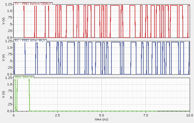
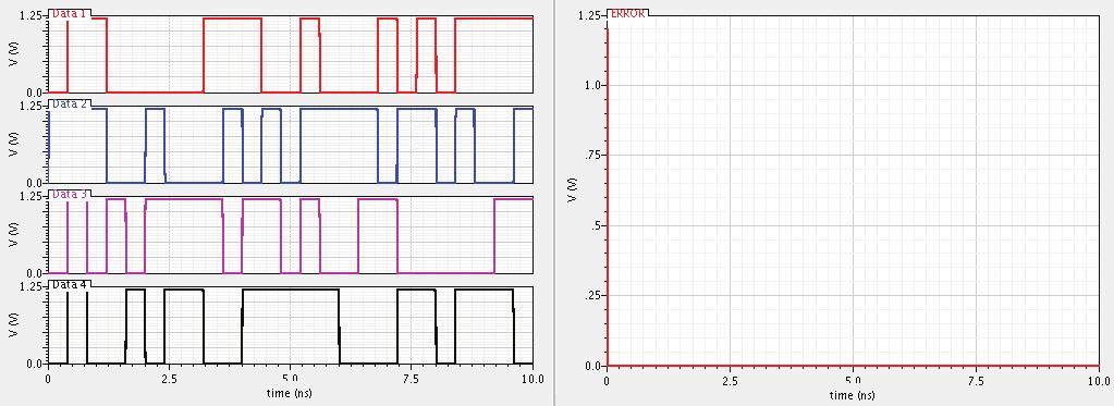
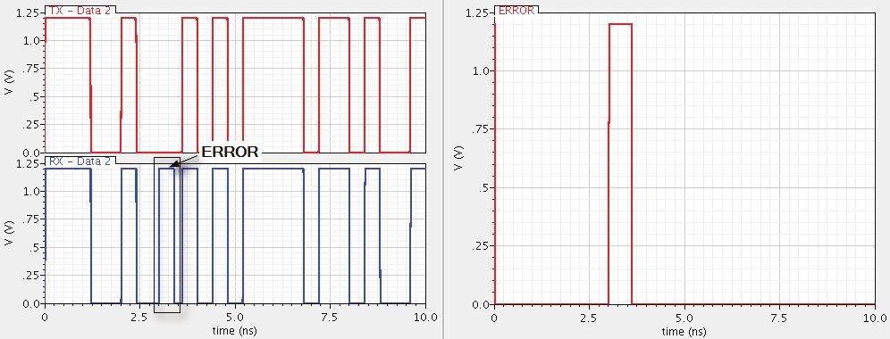
10 10 Pre-Lab 1. Assuming a 3-tap TX FIR equalizer with the z-domain transfer function as the following (13) Please find the low frequency response, Nyquist frequency response, and frequency peaking of this 3-tap TX FIR equalizer? 2. Design a passive CTLE as shown in Figure 7(a) to realize the transfer function as shown in Figure 12 using R1=900Ω. Please show your schematic. Figure 12 Passive CTLE Transfer Function 3. Design a 4-bit parallel PRBS generator with sequence length and an error detector circuit with a testing circuit at 2Gb/s with ideal blocks. Using the test circuit, you should be able to inject error data pattern and observe the error signal. An example is shown in Figure 13. Please show the simulation results. You may refer to the Appendix by Younghoon Song on how to build a parallel PRBS generator and detector. Figure 13 Parallel PRBS Testing Circuit
11 11 Questions 1. TX FIR Equalization. This problem investigates TX FIR equalization using the 12 Backplane channel peters_01_0605_b12_thru.s4p from course website. For parts (a) and (b), use the example MATLAB code channel_data_pulse_pda.m and produce the following 2 graphs: a) Peak-Distortion Eye Height versus FIR tap number at 4G, 8G, and 16Gbps (3 lines). For the tap numbers, use 1-tap (no equalization), 2-tap (1-post), 3-tap (1-pre and 1-post), and 4-tap (1-pre, 2-post). Don t restrict the TX equalizer resolution for this graph. b) 8Gb/s Peak-Distortion Eye Height versus Equalizer Resolution with 2, 3, and 4-tap equalization (3-lines). For the tap resolution sweep, use 3, 4, 5, 6 bits, and also include the infinite resolution data. Note: The above MATLAB code also requires the tx_eq.m function. Also, this MATLAB code is only a reference code. Feel free to modify and improve upon the code as you wish. c) Design an 8Gb/s TX Driver with Equalization [4]. Modify one of your drivers from Lab3 to include FIR equalization. i. The maximum output voltage swing can be anywhere from 300mVppd (min.) to 1Vppd (max.). This gives you the flexibility to choose whichever driver you wish from low-swing voltage-mode to current-mode. ii. iii. Use the results from part (a) and (b) to justify your tap number and resolution. Include two 8Gb/s PRBS eye diagrams one without equalization (all weight on main cursor) and one with the proper equalization taps enabled. Import the s- parameter file into your Cadence simulation to produce the eye diagrams. Make sure the channel is properly terminated at both ends. Note, as you will have some additional driver capacitance, the equalization taps may change slightly. iv. The driver and at least one pre-driver stage should be full-transistor level design. The other blocks (PRBS, delay elements, etc) can be macro-models. v. Report transmitter power consumption, power efficiency (mw/gb/s), and 8Gb/s eye height and width. 2. RX CTLE Equalization. Design an 8Gb/s active CTLE to meet the following specifications: a) Min peak gain at Nyquist (4GHz) of 6dB b) Zero frequency tunable from a minimum range of 500MHz to 1GHz c) Minimum tunable peaking (magnitude difference between Nyquist and low frequency response) range of 12dB (Example: +6dB at Nyquist frequency and -6dB at low frequency). d) Load capacitor = 25fF i. Produce frequency response plots showing the zero and peaking tunability. ii. Produce an 8Gb/s PRBS eye diagram with the 12 Backplane channel output as the input to the CTLE. Optimize the CTLE settings for optimal eye opening.
12 12 iii. Report CTLE power, power efficiency (mw/gb/s), and 8Gb/s eye height and width. 3. RX DFE Equalization. Design an 8Gb/s 2-tap DFE [2][3]. a) Use one of the comparators you designed in Lab4 in your design. Note, you probably have to speed this design up as you will need a 4GHz clock if you implement a halfrate design. b) The only thing that has to be transistor level is the comparator. The rest of the blocks (summer, feedback taps, other logic) can be macro-models. Note, for the summer model make sure to capture the RC settling if you use a linear resistive load summer. Feel free to investigate an integrating architecture if you prefer. c) Produce an 8Gb/s PRBS eye diagram at the summer output with the 12 Backplane channel output as the input to the DFE. Optimize the DFE settings for optimal eye opening at the input of the comparator (summer output). d) Report DFE power, power efficiency (mw/gb/s), and 8Gb/s eye height and width. e) Note, you have to synchronize the DFE with the incoming data stream. A good way to do this is with an initial lone pulse input pattern. Adjust your comparator clock to sample near the peak of the lone pulse. Then simulate with the PRBS data. References [1] Digital Systems Engineering, W. Dally and J. Poulton, Cambridge University Press, [2] R. Payne, et al., A 6.25-Gb/s binary transceiver in 0.13-um CMOS for serial data transmission across high loss legacy backplane channels, IEEE Journal of Solid-State Circuits, vol. 40, no. 12, Dec. 2005, pp [3] M. Park, J. Bulzacchelli, and D. Friedman, A 7 Gb/s 9.3 mw 2-tap current-integrating DFE receiver, in IEEE ISSCC Dig. Tech. Papers, Feb. 2007, pp [4] John F. Bulzacchelli, et al., A 10-Gb/s 5-Tap DFE/4-Tap FFE transceiver in 90-nm CMOS technology, IEEE Journal of Solid-State Circuits, vol. 41, no. 12, Dec. 2006, pp
13 Appendix 13
14 repared by: Younghoon Song
15
16
17
18
19
20
ECEN689: Special Topics in High-Speed Links Circuits and Systems Spring 2012
 ECEN689: Special Topics in High-Speed Links Circuits and Systems Spring 0 Lecture 8: RX FIR, CTLE, & DFE Equalization Sam Palermo Analog & Mixed-Signal Center Texas A&M University Announcements Exam is
ECEN720: High-Speed Links Circuits and Systems Spring 2017
 ECEN720: High-Speed Links Circuits and Systems Spring 207 Lecture 8: RX FIR, CTLE, DFE, & Adaptive Eq. Sam Palermo Analog & Mixed-Signal Center Texas A&M University Announcements Lab 4 Report and Prelab
A 5-Gb/s 156-mW Transceiver with FFE/Analog Equalizer in 90-nm CMOS Technology Wang Xinghua a, Wang Zhengchen b, Gui Xiaoyan c,
 4th International Conference on Computer, Mechatronics, Control and Electronic Engineering (ICCMCEE 2015) A 5-Gb/s 156-mW Transceiver with FFE/Analog Equalizer in 90-nm CMOS Technology Wang Xinghua a,
ECEN 720 High-Speed Links Circuits and Systems
 1 ECEN 720 High-Speed Links Circuits and Systems Lab4 Receiver Circuits Objective To learn fundamentals of receiver circuits. Introduction Receivers are used to recover the data stream transmitted by transmitters.
ECEN 720 High-Speed Links: Circuits and Systems
 1 ECEN 720 High-Speed Links: Circuits and Systems Lab4 Receiver Circuits Objective To learn fundamentals of receiver circuits. Introduction Receivers are used to recover the data stream transmitted by
EQUALIZERS. HOW DO? BY: ANKIT JAIN
 EQUALIZERS. HOW DO? BY: ANKIT JAIN AGENDA DFE (Decision Feedback Equalizer) Basics FFE (Feed-Forward Equalizer) Basics CTLE (Continuous-Time Linear Equalizer) Basics More Complex Equalization UNDERSTANDING
To learn S-parameters, eye diagram, ISI, modulation techniques and their simulations in MATLAB and Cadence.
 1 ECEN 720 High-Speed Links: Circuits and Systems Lab2- Channel Models Objective To learn S-parameters, eye diagram, ISI, modulation techniques and their simulations in MATLAB and Cadence. Introduction
ECEN 720 High-Speed Links: Circuits and Systems. Lab3 Transmitter Circuits. Objective. Introduction. Transmitter Automatic Termination Adjustment
 1 ECEN 720 High-Speed Links: Circuits and Systems Lab3 Transmitter Circuits Objective To learn fundamentals of transmitter and receiver circuits. Introduction Transmitters are used to pass data stream
A10-Gb/slow-power adaptive continuous-time linear equalizer using asynchronous under-sampling histogram
 LETTER IEICE Electronics Express, Vol.10, No.4, 1 8 A10-Gb/slow-power adaptive continuous-time linear equalizer using asynchronous under-sampling histogram Wang-Soo Kim and Woo-Young Choi a) Department
To learn S-parameter, eye diagram, ISI, modulation techniques and to simulate in Matlab and Cadence.
 1 ECEN 689 High-Speed Links Circuits and Systems Lab2- Channel Models Objective To learn S-parameter, eye diagram, ISI, modulation techniques and to simulate in Matlab and Cadence. Introduction S-parameters
High Speed I/O 2-PAM Receiver Design. EE215E Project. Signaling and Synchronization. Submitted By
 High Speed I/O 2-PAM Receiver Design EE215E Project Signaling and Synchronization Submitted By Amrutha Iyer Kalpana Manickavasagam Pritika Dandriyal Joseph P Mathew Problem Statement To Design a high speed
ECEN720: High-Speed Links Circuits and Systems Spring 2017
 ECEN72: High-Speed Links Circuits and Systems Spring 217 Lecture 4: Channel Pulse Model & Modulation Schemes Sam Palermo Analog & Mixed-Signal Center Texas A&M University Announcements & Agenda Lab 1 Report
Ultra-high-speed Interconnect Technology for Processor Communication
 Ultra-high-speed Interconnect Technology for Processor Communication Yoshiyasu Doi Samir Parikh Yuki Ogata Yoichi Koyanagi In order to improve the performance of storage systems and servers that make up
A 10Gbps Analog Adaptive Equalizer and Pulse Shaping Circuit for Backplane Interface
 Proceedings of the 5th WSEAS Int. Conf. on CIRCUITS, SYSTEMS, ELECTRONICS, CONTROL & SIGNAL PROCESSING, Dallas, USA, November 1-3, 2006 225 A 10Gbps Analog Adaptive Equalizer and Pulse Shaping Circuit
To learn statistical bit-error-rate (BER) simulation, BER link noise budgeting and using ADS to model high speed I/O link circuits
 simulation, BER link noise budgeting and using ADS to model high speed I/O link circuits") 1 ECEN 720 High-Speed Links: Circuits and Systems Lab6 Link Modeling with ADS Objective To learn statistical bit-error-rate (BER) simulation, BER link noise budgeting and using ADS to model high speed
1 ECEN 720 High-Speed Links: Circuits and Systems Lab6 Link Modeling with ADS Objective To learn statistical bit-error-rate (BER) simulation, BER link noise budgeting and using ADS to model high speed
IN HIGH-SPEED wireline transceivers, a (DFE) is often
 is often") 326 IEEE TRANSACTIONS ON CIRCUITS AND SYSTEMS II: EXPRESS BRIEFS, VOL. 59, NO. 6, JUNE 2012 Decision Feedback Equalizer Architectures With Multiple Continuous-Time Infinite Impulse Response Filters Shayan
326 IEEE TRANSACTIONS ON CIRCUITS AND SYSTEMS II: EXPRESS BRIEFS, VOL. 59, NO. 6, JUNE 2012 Decision Feedback Equalizer Architectures With Multiple Continuous-Time Infinite Impulse Response Filters Shayan
ECEN689: Special Topics in High-Speed Links Circuits and Systems Spring 2012
 ECEN689: Special Topics in High-Speed Links Circuits and Systems Spring 2012 Lecture 5: Termination, TX Driver, & Multiplexer Circuits Sam Palermo Analog & Mixed-Signal Center Texas A&M University Announcements
A 10Gb/s 10mm On-Chip Serial Link in 65nm CMOS Featuring a Half-Rate Time-Based Decision Feedback Equalizer
 A 10Gb/s 10mm On-Chip Serial Link in 65nm CMOS Featuring a Half-Rate Time-Based Decision Feedback Equalizer Po-Wei Chiu, Somnath Kundu, Qianying Tang, and Chris H. Kim University of Minnesota, Minneapolis,
ISSCC 2006 / SESSION 4 / GIGABIT TRANSCEIVERS / 4.1
 SSCC 006 / SESSON 4 / GGABT TRANSCEVERS / 4. 4. A 0Gb/s 5-Tap-/4-Tap-FFE Transceiver in 90nm CMOS M. Meghelli, S. Rylov, J. Bulzacchelli, W. Rhee, A. Rylyakov, H. Ainspan, B. Parker, M. Beakes, A. Chung,
56+ Gb/s Serial Transmission using Duobinary Signaling
 56+ Gb/s Serial Transmission using Duobinary Signaling Jan De Geest Senior Staff R&D Signal Integrity Engineer, FCI Timothy De Keulenaer Doctoral Researcher, Ghent University, INTEC-IMEC Introduction Motivation
A PROGRAMMABLE PRE-CURSOR ISI EQUALIZATION CIRCUIT FOR HIGH-SPEED SERIAL LINK OVER HIGHLY LOSSY BACKPLANE CHANNEL
 A PROGRAMMABLE PRE-CUROR II EQUALIZATION CIRCUIT FOR HIGH-PEED ERIAL LINK OVER HIGHLY LOY BACKPLANE CHANNEL Bo Wang, Dianyong Chen, Bangli Liang, Jinguang Jiang 2 and Tad Kwasniewski DOE, Carleton University,
5Gbps Serial Link Transmitter with Pre-emphasis
 Gbps Serial Link Transmitter with Pre-emphasis Chih-Hsien Lin, Chung-Hong Wang and Shyh-Jye Jou Department of Electrical Engineering,National Central University,Chung-Li, Taiwan R.O.C. Abstract- High-speed
To learn Statistical Bit-error-rate (BER) simulation, BERlink noise budgeting and usage of ADS to model high speed I/O link circuits.
 simulation, BERlink noise budgeting and usage of ADS to model high speed I/O link circuits.") 1 ECEN 720 High-Speed Links Circuits and Systems Lab6 Link Modeling with ADS Objective To learn Statistical Bit-error-rate (BER) simulation, BERlink noise budgeting and usage of ADS to model high speed
1 ECEN 720 High-Speed Links Circuits and Systems Lab6 Link Modeling with ADS Objective To learn Statistical Bit-error-rate (BER) simulation, BERlink noise budgeting and usage of ADS to model high speed
ECEN 620: Network Theory Broadband Circuit Design Fall 2012
 ECEN 620: Network Theory Broadband Circuit Design Fall 2012 Lecture 23: High-Speed I/O Overview Sam Palermo Analog & Mixed-Signal Center Texas A&M University Announcements Exam 3 is postponed to Dec. 11
EE290C Spring Lecture 5: Equalization Techniques. Elad Alon Dept. of EECS 9" FR4 26" FR4. 9" FR4, via stub.
 EE29C Spring 211 Lecture 5: Equalization Techniques Elad Alon Dept. of EECS Link Channels Attenuation [db] -1-2 -3-4 -5 9" FR4, via stub 9" FR4 26" FR4-6 26" FR4, via stub 2 4 6 8 1 frequency [GHz] EE29C
if the conductance is set to zero, the equation can be written as following t 2 (4)
") 1 ECEN 720 High-Speed Links: Circuits and Systems Lab1 - Transmission Lines Objective To learn about transmission lines and time-domain reflectometer (TDR). Introduction Wires are used to transmit clocks
1 ECEN 720 High-Speed Links: Circuits and Systems Lab1 - Transmission Lines Objective To learn about transmission lines and time-domain reflectometer (TDR). Introduction Wires are used to transmit clocks
High-Speed Circuits and Systems Laboratory B.M.Yu. High-Speed Circuits and Systems Lab.
 High-Speed Circuits and Systems Laboratory B.M.Yu 1 Content 1. Introduction 2. Pre-emphasis 1. Amplitude pre-emphasis 2. Phase pre-emphasis 3. Circuit implantation 4. Result 5. Conclusion 2 Introduction
Studies on FIR Filter Pre-Emphasis for High-Speed Backplane Data Transmission
 Studies on FIR Filter Pre-Emphasis for High-Speed Backplane Data Transmission Miao Li Department of Electronics Carleton University Ottawa, ON. K1S5B6, Canada Tel: 613 525754 Email:mili@doe.carleton.ca
An 8-Gb/s Inductorless Adaptive Passive Equalizer in µm CMOS Technology
 JOURNAL OF SEMICONDUCTOR TECHNOLOGY AND SCIENCE, VOL.12, NO.4, DECEMBER, 2012 http://dx.doi.org/10.5573/jsts.2012.12.4.405 An 8-Gb/s Inductorless Adaptive Passive Equalizer in 0.18- µm CMOS Technology
Source Coding and Pre-emphasis for Double-Edged Pulse width Modulation Serial Communication
 Source Coding and Pre-emphasis for Double-Edged Pulse width Modulation Serial Communication Abstract: Double-edged pulse width modulation (DPWM) is less sensitive to frequency-dependent losses in electrical
Transmission-Line-Based, Shared-Media On-Chip. Interconnects for Multi-Core Processors
 Design for MOSIS Educational Program (Research) Transmission-Line-Based, Shared-Media On-Chip Interconnects for Multi-Core Processors Prepared by: Professor Hui Wu, Jianyun Hu, Berkehan Ciftcioglu, Jie
A 0.18µm CMOS Gb/s Digitally Controlled Adaptive Line Equalizer with Feed-Forward Swing Control for Backplane Serial Link
 1 A 0.18µm CMOS 3.125-Gb/s Digitally Controlled Adaptive Line Equalizer with Feed-Forward Swing Control for Backplane Serial Link Ki-Hyuk Lee, Jae-Wook Lee nonmembers and Woo-Young Choi regular member
Delft University of Technology Faculty of Electrical Engineering, Mathematics and Computer Science
 Delft University of Technology Faculty of Electrical Engineering, Mathematics and Computer Science Analysis and Design of Decision Feedback Equalizers for bitrates of 10Gbps and Beyond in Submicron CMOS
Design Metrics for Blind ADC-Based Wireline Receivers
 Design Metrics for Blind ADC-Based Wireline Receivers (Invited Paper) Ali Sheikholeslami 1 and Hirotaka Tamura 2 1 Department of Electrical and Computer Engineering, University of Toronto, Canada, 2 Fujitsu
A Two-Tone Test Method for Continuous-Time Adaptive Equalizers
 Two-Tone Test Method for Continuous-Time daptive Equalizers Dongwoo Hong*, Shadi Saberi**, Kwang-Ting (Tim) Cheng*, C. Patrick Yue* University of California, Santa Barbara, C, US* Carnegie Mellon University,
QAM-Based Transceiver Solutions for Full-Duplex Gigabit Ethernet Over 4 Pairs of UTP-5 Cable. Motivation for Using QAM
 QAM-Based Transceiver Solutions for Full-Duplex Gigabit Ethernet Over 4 Pairs of UTP-5 Cable Henry Samueli, Jeffrey Putnam, Mehdi Hatamian Broadcom Corporation 16251 Laguna Canyon Road Irvine, CA 92618
ECEN620: Network Theory Broadband Circuit Design Fall 2014
 ECEN620: Network Theory Broadband Circuit Design Fall 2014 Lecture 19: High-Speed Transmitters Sam Palermo Analog & Mixed-Signal Center Texas A&M University Announcements Exam 3 is on Friday Dec 5 Focus
High-Speed Link Tuning Using Signal Conditioning Circuitry in Stratix V Transceivers
 High-Speed Link Tuning Using Signal Conditioning Circuitry in Stratix V Transceivers AN678 Subscribe This application note provides a set of guidelines to run error free across backplanes at high-speed
A 1.5 Gbps Transceiver Chipset in 0.13-mm CMOS for Serial Digital Interface
 JOURNAL OF SEMICONDUCTOR TECHNOLOGY AND SCIENCE, VOL.17, NO.4, AUGUST, 2017 ISSN(Print) 1598-1657 https://doi.org/10.5573/jsts.2017.17.4.552 ISSN(Online) 2233-4866 A 1.5 Gbps Transceiver Chipset in 0.13-mm
High-Speed Interconnect Technology for Servers
 High-Speed Interconnect Technology for Servers Hiroyuki Adachi Jun Yamada Yasushi Mizutani We are developing high-speed interconnect technology for servers to meet customers needs for transmitting huge
ECEN620: Network Theory Broadband Circuit Design Fall 2014
 ECEN620: Network Theory Broadband Circuit Design Fall 2014 Lecture 16: CDRs Sam Palermo Analog & Mixed-Signal Center Texas A&M University Announcements Project descriptions are posted on the website Preliminary
ECEN720: High-Speed Links Circuits and Systems Spring 2017
 ECEN720: High-Speed Links Circuits and Systems Spring 2017 Lecture 12: CDRs Sam Palermo Analog & Mixed-Signal Center Texas A&M University Announcements Project Preliminary Report #2 due Apr. 20 Expand
A 5-8 Gb/s Low-Power Transmitter with 2-Tap Pre-Emphasis Based on Toggling Serialization
 A 5-8 Gb/s Low-Power Transmitter with 2-Tap Pre-Emphasis Based on Toggling Serialization Sung-Geun Kim, Tongsung Kim, Dae-Hyun Kwon, and Woo-Young Choi Department of Electrical and Electronic Engineering,
BER-optimal ADC for Serial Links
 BER-optimal ADC for Serial Links Speaker Name: Yingyan Lin Co-authors: Min-Sun Keel, Adam Faust, Aolin Xu, Naresh R. Shanbhag, Elyse Rosenbaum, and Andrew Singer Advisor s name: Naresh R. Shanbhag Affiliation:
Analog CMOS Interface Circuits for UMSI Chip of Environmental Monitoring Microsystem
 Analog CMOS Interface Circuits for UMSI Chip of Environmental Monitoring Microsystem A report Submitted to Canopus Systems Inc. Zuhail Sainudeen and Navid Yazdi Arizona State University July 2001 1. Overview
ISSCC 2006 / SESSION 13 / OPTICAL COMMUNICATION / 13.2
 13.2 An MLSE Receiver for Electronic-Dispersion Compensation of OC-192 Fiber Links Hyeon-min Bae 1, Jonathan Ashbrook 1, Jinki Park 1, Naresh Shanbhag 2, Andrew Singer 2, Sanjiv Chopra 1 1 Intersymbol
3Gb/s CMOS Adaptive Equalizer for Backplane Serial Links
 3Gb/s CMOS Adaptive Equalizer for Backplane Serial Links JaeWook Lee and WooYoung Choi Department of Electrical and Electronic Engineering, Yonsei University patima@tera.yonsei.ac.kr Abstract A new line
Statistical Link Modeling
 April 26, 2018 Wendem Beyene UIUC ECE 546 Statistical Link Modeling Review of Basic Techniques What is a High-Speed Link? 1011...001 TX Channel RX 1011...001 Clock Clock Three basic building blocks: Transmitter,
A 5-Gbps USB3.0 transmitter and receiver linear equalizer
 INTERNATIONAL JOURNAL OF CIRCUIT THEORY AND APPLICATIONS Int. J. Circ. Theor. Appl. (2014) Published online in Wiley Online Library (wileyonlinelibrary.com)..1982 A 5-Gbps USB3.0 transmitter and receiver
HIGH-SPEED LOW-POWER ON-CHIP GLOBAL SIGNALING DESIGN OVERVIEW. Xi Chen, John Wilson, John Poulton, Rizwan Bashirullah, Tom Gray
 HIGH-SPEED LOW-POWER ON-CHIP GLOBAL SIGNALING DESIGN OVERVIEW Xi Chen, John Wilson, John Poulton, Rizwan Bashirullah, Tom Gray Agenda Problems of On-chip Global Signaling Channel Design Considerations
A 24Gb/s Software Programmable Multi-Channel Transmitter
 A 24Gb/s Software Programmable Multi-Channel Transmitter A. Amirkhany 1, A. Abbasfar 2, J. Savoj 2, M. Jeeradit 2, B. Garlepp 2, V. Stojanovic 2,3, M. Horowitz 1,2 1 Stanford University 2 Rambus Inc 3
ECEN689: Special Topics in High-Speed Links Circuits and Systems Spring 2012
 ECEN689: Special Topics in High-Speed Links Circuits and Systems Spring 2012 Lecture 6: RX Circuits Sam Palermo Analog & Mixed-Signal Center Texas A&M University Announcements Lab 4 Prelab due now Exam
ISSCC 2006 / SESSION 20 / WLAN/WPAN / 20.5
 20.5 An Ultra-Low Power 2.4GHz RF Transceiver for Wireless Sensor Networks in 0.13µm CMOS with 400mV Supply and an Integrated Passive RX Front-End Ben W. Cook, Axel D. Berny, Alyosha Molnar, Steven Lanzisera,
ECEN620: Network Theory Broadband Circuit Design Fall 2012
 ECEN620: Network Theory Broadband Circuit Design Fall 2012 Lecture 20: CDRs Sam Palermo Analog & Mixed-Signal Center Texas A&M University Announcements Exam 2 is on Friday Nov. 9 One double-sided 8.5x11
ISSCC 2003 / SESSION 20 / WIRELESS LOCAL AREA NETWORKING / PAPER 20.5
 ISSCC 2003 / SESSION 20 / WIRELESS LOCAL AREA NETWORKING / PAPER 20.5 20.5 A 2.4GHz CMOS Transceiver and Baseband Processor Chipset for 802.11b Wireless LAN Application George Chien, Weishi Feng, Yungping
A pJ/bit, 4.8-8Gb/s I/O Transceiver in 65nm-CMOS. Abstract
 A 0.47-0.66pJ/bit, 4.8-8Gb/s I/O Transceiver in 65nm-CMOS Young-Hoon Song, student member, IEEE, Rui Bai, student member, IEEE, Kangmin Hu, Member, IEEE, Hae-Woong Yang, student member, IEEE, Patrick Yin
Backchannel Modeling and Simulation Using Recent Enhancements to the IBIS Standard
 Backchannel Modeling and Simulation Using Recent Enhancements to the IBIS Standard By Ken Willis, Product Engineering Architect; Ambrish Varma, Senior Principal Software Engineer; Dr. Kumar Keshavan, Senior
ISSN:
 1391 DESIGN OF 9 BIT SAR ADC USING HIGH SPEED AND HIGH RESOLUTION OPEN LOOP CMOS COMPARATOR IN 180NM TECHNOLOGY WITH R-2R DAC TOPOLOGY AKHIL A 1, SUNIL JACOB 2 1 M.Tech Student, 2 Associate Professor,
MSAN B1Q Line Code Tutorial Application Note. Introduction. Line Coding
 2B1Q Line Code Tutorial Introduction Line Coding ISSUE 2 March 1990 In August 1986 the T1D1.3 (Now T1E1.4) technical subcommittee of the American National Standards Institute chose to base their standard
100 Gb/s: The High Speed Connectivity Race is On
 100 Gb/s: The High Speed Connectivity Race is On Cathy Liu SerDes Architect, LSI Corporation Harold Gomard SerDes Product Manager, LSI Corporation October 6, 2010 Agenda 100 Gb/s Ethernet evolution SoC
Xilinx Answer Link Tuning For UltraScale and UltraScale+
 Xilinx Answer 70918 Link Tuning For UltraScale and UltraScale+ Important Note: This downloadable PDF of an Answer Record is provided to enhance its usability and readability. It is important to note that
ADAPTIVE DECISION FEEDBACK EQUALIZATION FOR MULTI-Gbps DATA LINKS
 ADAPTIVE DECISION FEEDBACK EQUALIZATION FOR MULTI-Gbps DATA LINKS by Alaa R. Abdullah Bacelor of Science, University of Technology, Baghdad, Iraq, 1989 Master of Science, Ryerson University, Toronto, Canada,
Backplane Applications with 28 nm FPGAs
 Backplane Applications with 28 nm FPGAs WP-01185-1.1 White Paper This white paper covers the challenges of backplane applications and how to use the features of Altera Stratix V GX and GS FPGAs to address
A Low-Noise Programmable-Gain Amplifier for 25Gb/s Multi-Mode Fiber Receivers in 28 nm CMOS FDSOI
 A Low-Noise Programmable-Gain Amplifier for 25Gb/s Multi-Mode Fiber Receivers in 28 nm CMOS FDSOI F. Radice 1, M. Bruccoleri 1, E. Mammei 2, M. Bassi 3, A. Mazzanti 3 1 STMicroelectronics, Cornaredo, Italy
/$ IEEE
 IEEE TRANSACTIONS ON CIRCUITS AND SYSTEMS II: EXPRESS BRIEFS, VOL. 53, NO. 11, NOVEMBER 2006 1205 A Low-Phase Noise, Anti-Harmonic Programmable DLL Frequency Multiplier With Period Error Compensation for
A 10-Gb/s Multiphase Clock and Data Recovery Circuit with a Rotational Bang-Bang Phase Detector
 JOURNAL OF SEMICONDUCTOR TECHNOLOGY AND SCIENCE, VOL.16, NO.3, JUNE, 2016 ISSN(Print) 1598-1657 http://dx.doi.org/10.5573/jsts.2016.16.3.287 ISSN(Online) 2233-4866 A 10-Gb/s Multiphase Clock and Data Recovery
OIF CEI 6G LR OVERVIEW
 OIF CEI 6G LR OVERVIEW Graeme Boyd, Yuriy Greshishchev T10 SAS-2 WG meeting, Houston, 25-26 May 2005 www.pmc-sierra.com 1 Outline! Why CEI-6G LR is of Interest to SAS-2?! CEI-6G- LR Specification Methodology!
A 2-byte Parallel 1.25 Gb/s Interconnect I/O Interface with Self-configurable Link and Plesiochronous Clocking
 UDC 621.3.049.771.14:681.3.01 A 2-byte Parallel 1.25 Gb/s Interconnect I/O Interface with Self-configurable Link and Plesiochronous Clocking VKohtaroh Gotoh VHideki Takauchi VHirotaka Tamura (Manuscript
A 5Gb/s Speculative DFE for 2x Blind ADC-based Receivers in 65-nm CMOS. Siamak Sarvari
 A 5Gb/s Speculative DFE for 2x Blind ADC-based Receivers in 65-nm CMOS by Siamak Sarvari A thesis submitted in conformity with the requirements for the degree of Master of Applied Science Graduate Department
An Analog Phase-Locked Loop
 1 An Analog Phase-Locked Loop Greg Flewelling ABSTRACT This report discusses the design, simulation, and layout of an Analog Phase-Locked Loop (APLL). The circuit consists of five major parts: A differential
A 10-Gb/s Compact Low-Power Serial I/O With DFE-IIR Equalization in 65-nm CMOS
 A 10-Gb/s Compact Low-Power Serial I/O With DFE-IIR Equalization in 65-nm CMOS The MIT Faculty has made this article openly available. Please share how this access benefits you. Your story matters. Citation
06-011r0 Towards a SAS-2 Physical Layer Specification. Kevin Witt 11/30/2005
 06-011r0 Towards a SAS-2 Physical Layer Specification Kevin Witt 11/30/2005 Physical Layer Working Group Goal Draft a Specification which will: 1. Meet the System Designers application requirements, 2.
LSI and Circuit Technologies for the SX-8 Supercomputer
 LSI and Circuit Technologies for the SX-8 Supercomputer By Jun INASAKA,* Toshio TANAHASHI,* Hideaki KOBAYASHI,* Toshihiro KATOH,* Mikihiro KAJITA* and Naoya NAKAYAMA This paper describes the LSI and circuit
A Variable-Frequency Parallel I/O Interface with Adaptive Power Supply Regulation
 WA 17.6: A Variable-Frequency Parallel I/O Interface with Adaptive Power Supply Regulation Gu-Yeon Wei, Jaeha Kim, Dean Liu, Stefanos Sidiropoulos 1, Mark Horowitz 1 Computer Systems Laboratory, Stanford
A Complete 64Gb/s/lane Active Electrical Repeater. Yue Lu, Jaeduk Han, Nicholas Sutardja Prof. Elad Alon January 23, 2014
 A Complete 64Gb/s/lane Active Electrical Repeater Yue Lu, Jaeduk Han, Nicholas Sutardja Prof. Elad Alon January 23, 2014 The Electrical Signaling Challenge Required I/O speed rising dramatically, but power
ISSCC 2003 / SESSION 10 / HIGH SPEED BUILDING BLOCKS / PAPER 10.8
 ISSCC 2003 / SESSION 10 / HIGH SPEED BUILDING BLOCKS / PAPER 10.8 10.8 10Gb/s Limiting Amplifier and Laser/Modulator Driver in 0.18µm CMOS Technology Sherif Galal, Behzad Razavi Electrical Engineering
A Power-Scalable 7-Tap FIR Equalizer with Tunable Active Delay Line for 10-to-25Gb/s Multi-Mode Fiber EDC in 28nm LP-CMOS
 A Power-Scalable 7-Tap FIR Equalizer with Tunable Active Delay Line for 10-to-25Gb/s Multi-Mode Fiber EDC in 28nm LP-CMOS E. Mammei, F. Loi, F. Radice*, A. Dati*, M. Bruccoleri*, M. Bassi, A. Mazzanti
ISSCC 2003 / SESSION 4 / CLOCK RECOVERY AND BACKPLANE TRANSCEIVERS / PAPER 4.3
 ISSCC 2003 / SESSION 4 / CLOCK RECOVERY AND BACKPLANE TRANSCEIVERS / PAPER 4.3 4.3 A Second-Order Semi-Digital Clock Recovery Circuit Based on Injection Locking M.-J. Edward Lee 1, William J. Dally 1,2,
High-Performance Electrical Signaling
 High-Performance Electrical Signaling William J. Dally 1, Ming-Ju Edward Lee 1, Fu-Tai An 1, John Poulton 2, and Steve Tell 2 Abstract This paper reviews the technology of high-performance electrical signaling
A Pin and Power Efficient Low Latency 8-12Gb/s/wire 8b8w- Coded SerDes Link for High Loss Channels in 40nm Technology
 A Pin and Power Efficient Low Latency 8-12Gb/s/wire 8b8w- Coded SerDes Link for High Loss Channels in 40nm Technology Anant Singh 1, Dario Carnelli 1, Altay Falay 1, Klaas Hofstra 1, Fabio Licciardello
Electronic Dispersion Compensation of 40-Gb/s Multimode Fiber Links Using IIR Equalization
 Electronic Dispersion Compensation of 4-Gb/s Multimode Fiber Links Using IIR Equalization George Ng & Anthony Chan Carusone Dept. of Electrical & Computer Engineering University of Toronto Canada Transmitting
LOW-POWER HIGH-SPEED SERIAL LINK DESIGN
 LOW-POWER HIGH-SPEED SERIAL LINK DESIGN By JIKAI CHEN A DISSERTATION PRESENTED TO THE GRADUATE SCHOOL OF THE UNIVERSITY OF FLORIDA IN PARTIAL FULFILLMENT OF THE REQUIREMENTS FOR THE DEGREE OF DOCTOR OF
A 14-bit 2.5 GS/s DAC based on Multi-Clock Synchronization. Hegang Hou*, Zongmin Wang, Ying Kong, Xinmang Peng, Haitao Guan, Jinhao Wang, Yan Ren
 Joint International Mechanical, Electronic and Information Technology Conference (JIMET 2015) A 14-bit 2.5 GS/s based on Multi-Clock Synchronization Hegang Hou*, Zongmin Wang, Ying Kong, Xinmang Peng,
ADC-Based Backplane Receivers: Motivations, Issues and Future
 JOURNAL OF SEICONDUCTOR TECHNOLOGY AND SCIENCE, VOL.16, NO.3, JUNE, 2016 ISSN(Print) 1598-1657 http://dx.doi.org/10.5573/jsts.2016.16.3.300 ISSN(Online) 2233-4866 ADC-Based Backplane Receivers: otivations,
Comparison of Time Domain and Statistical IBIS-AMI Analyses Mike LaBonte SiSoft
 Comparison of Time Domain and Statistical IBIS-AMI Analyses Mike LaBonte SiSoft Asian IBIS Summit 2017 Taipei, ROC November 15, 2017 9 Combinations of TX and RX Model Types AMI file has: GetWave_Exists
Comparison of Time Domain and Statistical IBIS-AMI Analyses
 Comparison of Time Domain and Statistical IBIS-AMI Analyses Mike LaBonte SiSoft Asian IBIS Summit 2017 Shanghai, PRC November 13, 2017 9 Combinations of TX and RX Model Types AMI file has: GetWave_Exists
High-speed Integrated Circuits for Silicon Photonics
 High-speed Integrated Circuits for Silicon Photonics Institute of Semiconductor, CAS 2017.7 Outline Introduction High-Speed Signaling Fundamentals TX Design Techniques RX Design Techniques Design Examples
End-to-End System-Level Simulations with Repeaters for PCIe Gen4: A How-To Guide
 DesignCon 2017 End-to-End System-Level Simulations with Repeaters for PCIe Gen4: A How-To Guide Yongyao Li, Huawei liyongyao@huawei.com Casey Morrison, Texas Instruments cmorrison@ti.com Fangyi Rao, Keysight
Low Power Digital Receivers for Multi- Gb/s Wireline/Optical Communication
 Low Power Digital Receivers for Multi- Gb/s Wireline/Optical Communication by A K M Delwar Hossain A thesis submitted in partial fulfillment of the requirements for the degree of Master of Science in Integrated
A 2.4 GHZ RECEIVER IN SILICON-ON-SAPPHIRE MICHAEL PETERS. B.S., Kansas State University, 2009 A REPORT
 A 2.4 GHZ RECEIVER IN SILICON-ON-SAPPHIRE by MICHAEL PETERS B.S., Kansas State University, 2009 A REPORT submitted in partial fulfillment of the requirements for the degree MASTER OF SCIENCE Department
A 35 fj 10b 160 MS/s Pipelined- SAR ADC with Decoupled Flip- Around MDAC and Self- Embedded Offset Cancellation
 Y. Zu, C.- H. Chan, S.- W. Sin, S.- P. U, R.P. Martins, F. Maloberti: "A 35 fj 10b 160 MS/s Pipelined-SAR ADC with Decoupled Flip-Around MDAC and Self- Embedded Offset Cancellation"; IEEE Asian Solid-
High-Speed Transceiver Toolkit
 High-Speed Transceiver Toolkit Stratix V FPGA Design Seminars 2011 3.0 Stratix V FPGA Design Seminars 2011 Our seminars feature hour-long modules on different Stratix V capabilities and applications to
ISSCC 2004 / SESSION 25 / HIGH-RESOLUTION NYQUIST ADCs / 25.3
 ISSCC 2004 / SESSION 25 / HIGH-RESOLUTION NYQUIST ADCs / 25.3 25.3 A 96dB SFDR 50MS/s Digitally Enhanced CMOS Pipeline A/D Converter K. Nair, R. Harjani University of Minnesota, Minneapolis, MN Analog-to-digital
10 Mb/s Single Twisted Pair Ethernet Implementation Thoughts Proof of Concept Steffen Graber Pepperl+Fuchs
 10 Mb/s Single Twisted Pair Ethernet Implementation Thoughts Proof of Concept Steffen Graber Pepperl+Fuchs IEEE802.3 10 Mb/s Single Twisted Pair Ethernet Study Group 9/8/2016 1 Overview Signal Coding Analog
Phil Lehwalder ECE526 Summer 2011 Dr. Chiang
 Phil Lehwalder ECE526 Summer 2011 Dr. Chiang PLL (Phase Lock Loop) Dynamic system that produces a clock in response to the frequency and phase of an input clock by varying frequency of an internal oscillator.
Publication [P3] By choosing to view this document, you agree to all provisions of the copyright laws protecting it.
![Publication [P3] By choosing to view this document, you agree to all provisions of the copyright laws protecting it.](/thumbs/94/120865947.jpg "Publication [P3] By choosing to view this document, you agree to all provisions of the copyright laws protecting it.") Publication [P3] Copyright c 2006 IEEE. Reprinted, with permission, from Proceedings of IEEE International Solid-State Circuits Conference, Digest of Technical Papers, 5-9 Feb. 2006, pp. 488 489. This
Publication [P3] Copyright c 2006 IEEE. Reprinted, with permission, from Proceedings of IEEE International Solid-State Circuits Conference, Digest of Technical Papers, 5-9 Feb. 2006, pp. 488 489. This
T10/05-428r0. From: Yuriy M. Greshishchev, PMC-Sierra Inc. Date: 06 November 2005
 T10/05-428r0 SAS-2 channels analyses and suggestion for physical link requirements To: T10 Technical Committee From: Yuriy M. Greshishchev, PMC-Sierra Inc. (yuriy_greshishchev@pmc-sierra.com) Date: 06
Dedication. To Mum and Dad
 Dedication To Mum and Dad Acknowledgment Table of Contents List of Tables List of Figures A B A B 0 1 B A List of Abbreviations Abstract Chapter1 1 Introduction 1.1. Motivation Figure 1. 1 The relative
High-Speed Links. Agenda : High Speed Links
 High-Speed Links Vladimir Stojanovic (with slides from M. Horowitz, J. Zerbe, K.Yang and W. Ellersick) EE371 Lecture 16 Agenda : High Speed Links High-Speed Links, What,Where? Signaling Faster - Evolution»
Quad 12-Bit Digital-to-Analog Converter (Serial Interface)
") Quad 1-Bit Digital-to-Analog Converter (Serial Interface) FEATURES COMPLETE QUAD DAC INCLUDES INTERNAL REFERENCES AND OUTPUT AMPLIFIERS GUARANTEED SPECIFICATIONS OVER TEMPERATURE GUARANTEED MONOTONIC OVER
Quad 1-Bit Digital-to-Analog Converter (Serial Interface) FEATURES COMPLETE QUAD DAC INCLUDES INTERNAL REFERENCES AND OUTPUT AMPLIFIERS GUARANTEED SPECIFICATIONS OVER TEMPERATURE GUARANTEED MONOTONIC OVER