DC to 30GHz Broadband MMIC Low-Power Amplifier
|
|
|
- Britton Lawson
- 5 years ago
- Views:
Transcription
1 DC to 30GHz Broadband MMIC Low-Power Amplifier Features Integrated LFX technology: Simplified low-cost assembly Drain bias inductor not required Broadband 45GHz performance: Good gain (10 ± 1.25dB) 14.5dBm Psat, 11.5dBm P1dB Low Noise Figure (5.5dB) >30dB dynamic gain control Integrated power detector 100% DC, RF, and visually tested Size: 1640x1100um (64.6x43.3mil) ECCN 3A001.b.2.d Description The MMA033AA is a seven stage traveling wave amplifier. The amplifier features Microsemi active LFX (Low Frequency extension) circuitry designed to reduce the integration cost of the amplifier. LFX eliminates the need for an off-chip bias choke (drain inductor) for low-frequency operation, simplifying and greatly reducing the cost of assembly. Application The MMA033AA Broadband MMIC Amplifier with LFX is designed for inexpensive integration in broadband applications in RF and microwave communications, test equipment and military systems. Key Characteristics: Vdd=7V, Idd=85mA, Zo=50Ω Specifications pertain to wafer measurements with RF probes and DC bias 25 C GHz GHz Parameter Description Min Typ Max Min Typ Max S21 (db) Small Signal Gain Flatness (±db) Gain Flatness S11 (db Input Match S22 (db) Output Match S12 (db) Reverse Isolation P1dB (dbm) 1dB Compressed Output Power Psat (dbm) Saturated Output Power NF (db) Noise Figure RFdet (mv/mw) RF Detector Sensitivity of 6


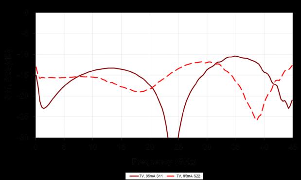
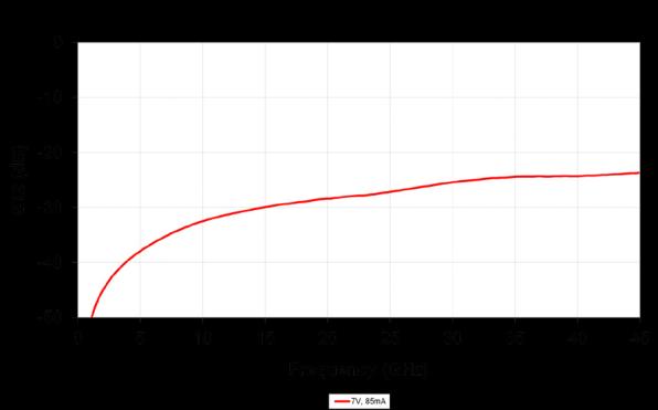
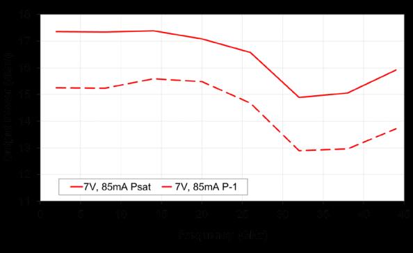
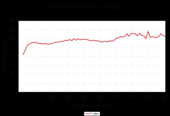
2 S21 Noise Figure Typical IC performance with package de-embedded S11, S22 S12 Output Power Group Delay 2 of 6
3 Table 1: Supplemental Specifications Parameter Description Min Typ Max Vdd Drain Bias Voltage 5V 7V 7.5V Idd Drain Bias Current - 85mA 120mA Vg1 1st Gate Bias Voltage -4V V Vg2 2nd Gate Bias Voltage Vdd-Vg2<7V N/C +4V P in Input Power (CW) dBm P dc Power Dissipation W - T ch Channel Temperature C Q ch Thermal Resistance (Tcase=85 C) - 22 C/W - Caution, ESD Sensitive Device 3 of 6
4 DC Bias: The MMA033AA features a patented on-chip active bias circuit called LFX. This circuit provides DC bias to the TWA drains without affecting RF performance; traditional biasing requires off-chip decoupling that increases the assembly complexity and cost. The device is biased by applying a positive voltage to the drain (Vdd), then setting the drain current (Idd) using a negative voltage on the gate (Vg1). The nominal bias is Vdd=7.0V, Idd=85mA; this will typically bring RFout (and the drain sense) to 4.5V. Improved performance can be achieved with gate bias adjustment; use the drain termination bypass to alter the output voltage (detected from the drain voltage sense). Gain Control: Dynamic gain control is available when operating the amplifier in the linear gain region. Negative voltage applied to the second gate (Vg2) reduces amplifier gain. RF Power Detection: RF output power can be calculated from the difference between the RF detector voltage and the DC detector voltage, minus a DC offset. Please consult the power detector application note available from the Microsemi webpage. Low-Frequency Use: The MMA033AA has been designed so that the bandwidth can be extended to low frequencies. The low end corner frequency of the device is primarily determined by the external biasing and AC coupling circuitry. Matching: The amplifier incorporates an on- chip termination resistor on the RF input, which is RF grounded with a small on-chip capacitor that goes open at frequencies below 1GHz. Gate termination bypass pads are provided for an external capacitor required for input match during low-frequency operation. The RF output is RF grounded through the bypass capacitor connected to the drain bias pad (Vdd). This capacitor will maintain the output match to low-mhz operating frequencies. For operation below 1GHz, a second bypass capacitor must be connected to the drain termination bypass, as shown in the assembly diagrams. DC Blocks: The amplifier is DC coupled to the RF input and output pads; DC voltage on these pads must be isolated from external circuitry. For operation above 2GHz, a series DC-blocking capacitor with minimum value of 20pF is recommended; operation at 40MHz requires a minimum of 120pF. Bias Inductor: The patented on-chip LFX circuit eliminates the need for a drain bias choke; the amplifier requires a bypass capacitor close to the chip and bonded to the drain bias pad. The drain bias supply is connected directly to the bypass capacitor. 4 of 6
 Pick-up and Chip Handling: This MMIC has exposed air bridges on the top surface. Do not pick up chip with vacuum on the die center; handle from edges or with a collet.")

5 Die size, pad locations, and pad descriptions Chip size: 1640x1100um (64.6x43.3mil) Chip size tolerance: ±5um (0.2mil) Chip thickness: 100 ±10um (4 ±0.4mil) Pad dimensions: 80x80um (3.1x3.1mil) Pick-up and Chip Handling: This MMIC has exposed air bridges on the top surface. Do not pick up chip with vacuum on the die center; handle from edges or with a collet. Thermal Heat Sinking: To avoid damage and for optimum performance, you must observe the maximum channel temperature and ensure adequate heat sinking. ESD Handling and Bonding: This MMIC is ESD sensitive; preventive measures should be taken during handling, die attach, and bonding. Epoxy die attach is recommended. Please review our application note MM-APP-0001 on our website for more handling, die attach and bonding information. 5 of 6
6 Information contained in this document is proprietary to Microsem. This document may not be modified in any way without the express written consent of Microsemi. Product processing does not necessarily include testing of all parameters. Microsemi reserves the right to change the configuration and performance of the product and to discontinue product at any time. Microsemi Corporate Headquarters Microsemi Corporation (Nasdaq: MSCC) offers a comprehensive portfolio of semiconductor One Enterprise, Aliso Viejo CA USA and system solutions for communications, defense and security, aerospace, and industrial Within the USA: +1 (949) markets. Products include high-performance and radiation-hardened analog mixed-signal Sales: +1 (949) integrated circuits, FPGAs, SoCs, and ASICs; power management products; timing and Fax: +1 (949) synchronization devices and precise time solutions, setting the world s standard for time; voice processing devices; RF solutions; discrete components; security technologies and scalable anti-tamper products; Power-over-Ethernet ICs and midspans; as well as custom design capabilities and services. Microsemi is headquartered in Aliso Viejo, Calif. and has approximately 3,400 employees globally. Learn more at Microsemi Corporation. All rights reserved. Microsemi and the Microsemi logo are trademarks of Microsemi Corporation. All other trademarks and service marks are the property of their respective owners. 6 of 6
7 Mouser Electronics Authorized Distributor Click to View Pricing, Inventory, Delivery & Lifecycle Information: Microsemi: MMA033AA
DC to 30GHz Broadband MMIC Low-Noise Amplifier
 DC to 30GHz Broadband MMIC Low-Noise Amplifier Features Great 0.04-30GHz performance: Flat gain (10.25 ± 0.75dB) High Psat at 30GHz (21dBm) High P1dB at 30GHz (18dBm) Excellent input / output return loss
DC to 30GHz Broadband MMIC Low-Power Amplifier
 DC to 30GHz Broadband MMIC Low-Power Amplifier Features Very low power dissipation: 4.5V, 85mA (383mW) High drain efficiency (43dBm/W) Good 1.5-20GHz performance: Flat gain (11 ± 0.75dB) 16.5dBm Psat,
DC to 30GHz Broadband MMIC Low-Noise Amplifier
 DC to 30GHz Broadband MMIC Low-Noise Amplifier Features Low noise, ultra-flat gain 6-20GHz: 2.5dB NF, 18 ± 0.3dB gain Excellent 1.5-20GHz performance: Very flat gain (17 ± 0.6dB) High Psat at 20GHz (20dBm)
DC to 45 GHz MMIC Amplifier
 DC to 45 GHz MMIC Amplifier Features 22 dbm Psat (8.5V p-p) Dynamic Gain Control 10 db Gain Low Noise Figure (5 db) Flatness ± 1dB to 40 GHz >18 dbm Pout @ >7 db Gain @ 45 GHz Size: 1640 x 835 µm ECCN
5-20GHz MMIC Amplifier with Integrated Bias
 5-20GHz MMIC Amplifier with Integrated Bias Features Excellent performance 5-18GHz: High, flat gain (15 ± 0.5dB) Good return loss (15dB) 17.5dBm P1dB, 20dBm Psat Mixed-signal 3.3V operation: Similar small-signal
2-20GHz, 12.5dB Gain Low-Noise Wideband Distributed Amplifier
 2-20GHz, 12.5dB Gain Low-Noise Wideband Distributed Amplifier Features >16.5dBm P 1dB with 1.9dB NF and 12.5dB gain at 10GHz
DC-22GHz, 16dB Gain Low-Noise Wideband Distributed Amplifier
 DC-22GHz, 16dB Gain Low-Noise Wideband Distributed Amplifier Features Excellent combination of wide bandwidth, low noise and high associated gain 1.7dB NF with >15.5dB gain at 10GHz Output IP3 ~26-29dBm
MMA051PP45 Datasheet. DC 22 GHz 1W GaAs MMIC phemt Distributed Power Amplifier
 MMA051PP45 Datasheet DC 22 GHz 1W GaAs MMIC phemt Distributed Power Amplifier Microsemi makes no warranty, representation, or guarantee regarding the information contained herein or the suitability of
DC-15 GHz Programmable Integer-N Prescaler
 DC-15 GHz Programmable Integer-N Prescaler Features Wide Operating Range: DC-20 GHz for Div-by-2/4/8 DC-15 GHz for Div-by-4/5/6/7/8/9 Low SSB Phase Noise: -153 dbc @ 10 khz Large Output Swings: >1 Vppk/side
1011GN-1200V 1200 Watts 50 Volts 32us, 2% L-Band Avionics 1030/1090 MHz
 GENERAL DESCRIPTION The 1011GN-1200V is an internally matched, COMMON SOURCE, class AB, GaN on SiC HEMT transistor capable of providing over 18.5 db gain, 1200 Watts of pulsed RF output power at 32us,
Using the Peak Detector Voltage to Compensate Output Voltage Change over Temperature
 Using the Peak Detector Voltage to Compensate Output Voltage Change over Temperature This document explains how to use the driver amplifier s peak detector to compensate the amplifier s output voltage
1011GN-1600VG 1600 Watts 50/52 Volts 32us, 2% L-Band Avionics 1030/1090 MHz
 GENERAL DESCRIPTION The 1030/1090MHz, 50V or 52V 1011GN-1600VG is an internally matched, common source, class AB, GaN on SiC HEMT transistor capable of providing greater than 1600 Watts of pulsed output
0912GN-50LE/LEL/LEP 50 Watts 50 Volts 32us, 2% & MIDS MHz
 E Class Earless Driver GaN Transistor Key Features 960-1215MHz 50W Pulsed Output Power 32µS-2% and MIDS Pulsing Common Source Class AB 50V Bias Voltage >60% Efficiency Across the Frequency Band under MIDS
AMMC KHz 40 GHz Traveling Wave Amplifier
 AMMC- 3 KHz GHz Traveling Wave Amplifier Data Sheet Chip Size: Chip Size Tolerance: Chip Thickness: Pad Dimensions: 3 x µm (9. x 1.3 mils) ± µm (±. mils) ± µm ( ±. mils) 8 x 8 µm (.9 ±. mils) Description
Features. = +25 C, Vdd = 5V
 v1.1 AMPLIFIER, 3. - 7. GHz Typical Applications The HMC39A is ideal for: Point-to-Point Radios VSAT LO Driver for HMC Mixers Military EW, ECM, C 3 I Space Functional Diagram Features Gain: 17. db Noise
CMD GHz Distributed Driver Amplifier. Features. Functional Block Diagram. Description
 Features Functional Block Diagram Wide bandwidth High linearity Single positive supply voltage On chip bias choke Vdd Description RFOUT The CMD97 is a wideband GaAs MMIC driver amplifier ideally suited
MPS Datasheet 100 MHz to 3 GHz RoHS Compliant 40 Watt Monolithic SPST PIN Switch
 MPS4103-607 Datasheet 100 MHz to 3 GHz RoHS Compliant 40 Watt Monolithic SPST PIN Switch Microsemi Corporate Headquarters One Enterprise, Aliso Viejo, CA 92656 USA Within the USA: +1 (800) 713-4113 Outside
500mA Negative Adjustable Regulator
 /SG137 500mA Negative Adjustable Regulator Description The family of negative adjustable regulators deliver up to 500mA output current over an output voltage range of -1.2 V to -37 V. The device includes
5 - Volt Fixed Voltage Regulators
 SG09 5 - Volt Fixed Voltage Regulators Description The SG09 is a self-contained 5V regulator designed to provide local regulation at currents up to A for digital logic cards. This device is available in
LX V Octal Series Diode Pairs Array with Redundancy. Description. Features. Applications
 LX0 V Octal Series Diode Pairs Array with Redundancy Description The LX0 is a diode array that features high breakdown voltage diodes with ESD protection and built-in redundancy. The array contains series
CMD GHz GaN Low Noise Amplifier. Features. Functional Block Diagram. Description
 Features Functional Block Diagram Ultra wideband performance Low noise figure High RF power survivablility Low current consumption Small die size Vdd Vgg2 RFOUT Description RFIN The CMD2 is a wideband
CMD GHz Low Noise Amplifier. Features. Functional Block Diagram. Description
 Features Functional Block Diagram Ultra low noise performance High linearity Small die size 2 GB 3 Vgg Vdd 4 RFIN RFOUT Description The CMD63 is a high dynamic range GaAs MMIC low noise amplifier ideally
Features. = +25 C, Vdd 1, 2, 3 = +3V
 v.11 HMC6LC AMPLIFIER, 6-2 GHz Typical Applications The HMC6LC is ideal for use as a LNA or driver amplifier for: Point-to-Point Radios Point-to-Multi-Point Radios & VSAT Test Equipment and Sensors Military
CMD GHz Distributed Low Noise Amplifier RFIN
 - GHz Distributed Low Noise Amplifier Features Wide bandwidth Single positive supply voltage Low noise figure Small die size Description Applications Wideband communication systems Point-to-point radios
CMD GHz Low Noise Amplifier
 Features Functional Block Diagram Ultra low noise figure High gain broadband performance Single supply voltage: +3. V @ 5 ma Small die size Vdd Description The CMD7 is a broadband MMIC low noise amplifier
CMD GHz Driver Amplifier. Features. Functional Block Diagram. Description
 Features Functional Block Diagram Wideband performance High gain High linearity HMC98 replacement Small die size RFIN Vdd1 Vdd Vdd3 RFOUT Description The CMD91 is a wideband GaAs MMIC driver amplifier
Features. Gain: 15.5 db. = +25 C, Vdd = 5V
 Typical Applications v2.97 Features AMPLIFIER, 3.5-7. GHz The HMC392 is ideal for: Gain: 5.5 db Point-to-Point Radios VSAT LO Driver for HMC Mixers Military EW, ECM, C 3 I Space Functional Diagram Noise
2 3 ACG1 ACG2 RFIN. Parameter Min Typ Max Units Frequency Range
 Features Functional Block Diagram Ultra wideband performance High linearity High output power Excellent return losses Small die size 2 3 ACG1 ACG2 RFOUT & Vdd Description RFIN 1 The is wideband GaAs MMIC
2 3 ACG1 ACG2 RFIN. Parameter Min Typ Max Units Frequency Range
 Features Functional Block Diagram Ultra wideband performance High linearity High output power Excellent return losses Small die size 2 3 ACG1 ACG2 RFOUT & Vdd Description RFIN 1 The CMD29 is wideband GaAs
Data Sheet. AMMC GHz Amplifier. Description. Features. Applications
 AMMC - 518-2 GHz Amplifier Data Sheet Chip Size: 92 x 92 µm (.2 x.2 mils) Chip Size Tolerance: ± 1µm (±.4 mils) Chip Thickness: 1 ± 1µm (4 ±.4 mils) Pad Dimensions: 8 x 8 µm (.1 x.1 mils or larger) Description
TGA4811. DC - 60 GHz Low Noise Amplifier
 TGA11 DC - GHz Low Noise Amplifier Key Features GHz Bandwidth 3. db noise figure > 15 db small signal gain 13 dbm P1dB +/- 7 ps group delay variation Bias:.5V, 5 ma.15 um 3MI mhemt Technology Chip Dimensions:
CMD GHz GaN Low Noise Amplifier. Features. Functional Block Diagram. Description
 Features Functional Block Diagram High gain Low noise figure High linearity High RF power survivability Small die size Description Vdd The CMD9 is a broadband MMIC GaN low noise amplifier ideally suited
CMD GHz Low Noise Amplifier. Functional Block Diagram. Features. Description
 33- GHz Low Noise Amplifier Features Functional Block Diagram Ultra low noise performance All positive bias Low current consumption Small die size 2 3 Vgg GB RFIN Vdd RFOUT Description The CMD9 is a highly
CMD217. Let Performance Drive GHz GaN Power Amplifier
 Let Performance Drive Features High Power High linearity Excellent efficiency Small die size Applications Ka-band communications Commercial satellite Military and space Description Functional Block Diagram
Very Low Stray Inductance Phase Leg SiC MOSFET Power Module
 MSCMC120AM03CT6LIAG Datasheet Very Low Stray Inductance Phase Leg SiC MOSFET Power Module Final May 2018 Contents 1 Revision History... 1 1.1 Revision A... 1 2 Product Overview... 2 2.1 Features... 2 2.2
Features. Gain: 17 db. OIP3: 25 dbm. = +25 C, Vdd 1, 2 = +3V
 v.7 HMCLC Typical Applications The HMCLC is ideal for use as a LNA or driver amplifier for: Point-to-Point Radios Point-to-Multi-Point Radios & VSAT Test Equipment and Sensors Military & Space Functional
Features. = +25 C, Vdd1, 2, 3 = 5V, Idd = 250 ma*
 v.4 HMC498LC4 Typical Applications Features The HMC498LC4 is ideal for use as a LNA or Driver amplifier for: Point-to-Point Radios Point-to-Multi-Point Radios & VSAT Test Equipment & Sensors Military End-Use
Features. Applications. Symbol Parameters/Conditions Units Min. Max.
 AMMC - 622 6-2 GHz Low Noise Amplifier Data Sheet Chip Size: 17 x 8 µm (67 x 31. mils) Chip Size Tolerance: ± 1 µm (±.4 mils) Chip Thickness: 1 ± 1 µm (4 ±.4 mils) Pad Dimensions: 1 x 1 µm (4 ±.4 mils)
3 4 ACG1 ACG2. 2 Vgg2 RFIN. Parameter Min Typ Max Units. Frequency Range DC - 24 GHz. Gain 18 db. Noise Figure 2.5 db. Output P1dB 25 dbm
 Features Ultra wideband performance Positive gain slope High output power Low noise figure Small die size Description The CMD44 is wideband GaAs MMIC distributed amplifier die which operates from DC to
Quantum SA.45s CSAC Chip Scale Atomic Clock
 Quantum SA.45s CSAC Chip Scale Atomic Clock Microsemi invented portable atomic timekeeping with QUANTUM TM, the world s first family of miniature and chip scale atomic clocks. Choose QUANTUM TM class for
3 4 ACG1 ACG2. Vgg2 2 RFIN. Parameter Min Typ Max Units Frequency Range
 Features Functional Block Diagram Ultra wideband performance Positive gain slope High output power Low noise figure Small die size 3 4 ACG ACG Vgg RFOUT & Vdd Description RFIN The CMD9 is wideband GaAs
APT80SM120B 1200V, 80A, 40mΩ
 V, A, mω Package Silicon Carbide N-Channel Power MOSFET TO-247 DESCRIPTION Silicon carbide (SiC) power MOSFET product line from Microsemi increase your performance over silicon MOSFET and silicon IGBT
CMD GHz Low Noise Amplifier. Functional Block Diagram. Features. Description
 Features Functional Block Diagram Ultra low noise performance Low current consumption Small die size GB 3 Vgg Vdd 4 RFIN RFOUT Description The CMD6 is a highly efficient GaAs MMIC low noise amplifier ideally
Features dbm
 v9.917 HMC441 Typical Applications Features The HMC441 is ideal for: Point-to-Point and Point-to-Multi-Point Radios VSAT LO Driver for HMC Mixers Military EW & ECM Functional Diagram Gain:.5 db Saturated
MMA GHz 1W Traveling Wave Amplifier Data Sheet
 Features: Frequency Range:.1 2 GHz P3dB: +29 dbm Gain: 12.5 db Vdd =12 V Ids =5 ma Input and Output Fully Matched to 5 Ω Applications: Fiber optics communication systems Microwave and wireless communication
MMA R4 30KHz-50GHz Traveling Wave Amplifier Data Sheet October 2012
 Features: Frequency Range: 30KHz 40 GHz P1dB: +22 dbm Vout: 7V p-p @50Ω Gain: 13.5 db Vdd =7 V Ids = 200 ma Input and Output Fully Matched to 50 Ω In 4x4mm QFN package Applications: Fiber optics communication
Ultrafast Soft Recovery Rectifier Diode
 APT30DQ60BG Datasheet Ultrafast Soft Recovery Rectifier Diode Final March 2018 Contents 1 Revision History... 1 1.1 Revision E... 1 1.2 Revision D... 1 1.3 Revision C... 1 1.4 Revision B... 1 1.5 Revision
MMA GHz, 0.1W Gain Block
 Total Size: 172 x 76 Scribe Alley: 7 x 7 MMA-174321 Features: Frequency Range: 17 43 GHz P1dB: 21 dbm Psat: 22 dbm Gain: 22 db Vdd =5 V (3 V to 5 V) Ids = 2 ma (15mA to 3mA) Input and Output Fully Matched
HMC994A AMPLIFIERS - LINEAR & POWER - CHIP. GaAs phemt MMIC 0.5 WATT POWER AMPLIFIER, DC - 30 GHz. Features. Typical Applications
 v3.218 HMC994A.5 WATT POWER AMPLIFIER, DC - 3 GHz Typical Applications The HMC994A is ideal for: Test Instrumentation Military & Space Fiber Optics Functional Diagram Features High P1dB Output Power: dbm
HMC618ALP3E AMPLIFIERS - LOW NOISE - SMT. GaAs SMT phemt LOW NOISE AMPLIFIER, GHz. Typical Applications. Features. Functional Diagram
 7 Typical Applications The is ideal for: Cellular/3G and LTE/WiMAX/4G BTS & Infrastructure Repeaters and Femto Cells Public Safety Radios Functional Diagram v. Electrical Specifications T A = + C, Rbias
SimpliPHY Transformerless Ethernet Designs
 ENT-AN0114 Application Note SimpliPHY Transformerless Ethernet Designs June 2018 Contents 1 Revision History... 1 1.1 Revision 2.0... 1 1.2 Revision 1.2... 1 1.3 Revision 1.1... 1 1.4 Revision 1.0... 1
Quantum SA.45s CSAC Chip Scale Atomic Clock
 Quantum SA.45s CSAC Chip Scale Atomic Clock Microsemi invented portable atomic timekeeping with QUANTUM TM, the world s first family of miniature and chip scale atomic clocks. Choose QUANTUM TM class for
OBSOLETE HMC5846LS6 AMPLIFIERS - LINEAR & POWER - SMT. Electrical Specifications, T A. Features. Typical Applications. General Description
 v1.414 Typical Applications The HMC846LS6 is ideal for: Point-to-Point Radios Point-to-Multi-Point Radios VSAT & SATCOM Military & Space Functional Diagram Electrical Specifications, T A = +2 C Vdd = Vdd1,
50 GHz to 95 GHz, GaAs, phemt, MMIC, Wideband Power Amplifier ADPA7001CHIPS
 FEATURES Gain:.5 db typical at 5 GHz to 7 GHz S11: db typical at 5 GHz to 7 GHz S: 19 db typical at 5 GHz to 7 GHz P1dB: 17 dbm typical at 5 GHz to 7 GHz PSAT: 1 dbm typical OIP3: 5 dbm typical at 7 GHz
Features. = +25 C, Vdd = 5V, Vgg1 = Vgg2 = Open
 v3.117 HMC441LM1 Typical Applications The HMC441LM1 is a medium PA for: Point-to-Point Radios Point-to-Multi-Point Radios VSAT LO Driver for HMC Mixers Military EW & ECM Functional Diagram Vgg1, Vgg2:
User Guide. NX A Single Channel Mobile PWM Switching Regulator Evaluation Board
 User Guide NX9548 9 A Single Channel Mobile PWM Switching Regulator Evaluation Board Contents 1 Revision History... 1 1.1 Revision 1.0... 1 2 Product Overview... 2 2.1 Key Features... 2 2.2 Applications...
HMC906A. Amplifiers - Linear & Power - CHIP. Electrical Specifications, T A. Typical Applications. Features. General Description. Functional Diagram
 Typical Applications Features The HMC96A is ideal for: Satellite Communications Point-to-Point Radios Point-to-Multi-Point Radios VSAT Military & Space Functional Diagram Saturated Output Power: +33.5
Features = +5V. = +25 C, Vdd 1. = Vdd 2
 v7.11 HMC1LC3 POWER AMPLIFIER, - GHz Typical Applications The HMC1LC3 is ideal for use as a medium power amplifier for: Microwave Radio & VSAT Military & Space Test Equipment & Sensors Fiber Optics LO
Low-Jitter, Precision Clock Generator with Two Outputs
 19-2456; Rev 0; 11/07 E V A L U A T I O N K I T A V A I L A B L E Low-Jitter, Precision Clock Generator Ethernet Networking Equipment General Description The is a low-jitter precision clock generator optimized
APT80SM120J 1200V, 56A, 40mΩ Package APT80SM120J
 APT8SM12J 12V, 56A, 4mΩ Package APT8SM12J PRELIMINARY Silicon Carbide N-Channel Power MOSFET DESCRIPTION Silicon carbide (SiC) power MOSFET product line from Microsemi increase your performance over silicon
QUAD POWER FAULT MONITOR
 SG154 QUAD POWER FAULT MONITOR Description The SG154 is an integrated circuit capable of monitoring up to four positive DC supply voltages simultaneously for overvoltage and undervoltage fault conditions.
Analog Devices Welcomes Hittite Microwave Corporation NO CONTENT ON THE ATTACHED DOCUMENT HAS CHANGED
 Analog Devices Welcomes Hittite Microwave Corporation NO CONTENT ON THE ATTACHED DOCUMENT HAS CHANGED www.analog.com www.hittite.com THIS PAGE INTENTIONALLY LEFT BLANK v1.414 Typical Applications The HMC5846LS6
Features OUT E S T CODE. = +25 C, Vdd= 8V, Idd= 60 ma*
 E S T CODE E S T CODE v1.818 HMC6 AMPLIFIER, DC - 2 GHz Typical Applications Features The HMC6 is ideal for: Noise Figure: 2.5 db @ 1 GHz Telecom Infrastructure Microwave Radio & VSAT Military & Space
SURFACE MOUNT PHEMT 2 WATT POWER AMPLIFIER,
 v2.617 AMPLIFIER, - 12 GHz Typical Applications The is ideal for use as a power amplifier for: Point-to-Point Radios Point-to-Multi-Point Radios Test Equipment and Sensors Military End-Use Features Saturated
Data Sheet AMMC KHz 80 GHz TWA. Description. Features. Typical Performance (Vd=5V, Idsq=0.1A) Component Image.
 Component Image.") AMMC-525 3KHz 8 GHz TWA Data Sheet Description The AMMC-525 MMIC is a 3KHz to 8GHz ultra broadband traveling wave amplifier. In this operational frequency band, AMMC-525 provides 8dB gain with better than
AMMC-525 3KHz 8 GHz TWA Data Sheet Description The AMMC-525 MMIC is a 3KHz to 8GHz ultra broadband traveling wave amplifier. In this operational frequency band, AMMC-525 provides 8dB gain with better than
Features. = +25 C, Vdd = +15V, Vgg2 = +9.5V [1], Idq = 500 ma [2]
![Features. = +25 C, Vdd = +15V, Vgg2 = +9.5V [1], Idq = 500 ma [2]](/thumbs/88/115381636.jpg "Features. = +25 C, Vdd = +15V, Vgg2 = +9.5V [1], Idq = 500 ma [2]") v3.41 Typical Applications Features The is ideal for: Test Instrumentation Military & Space Fiber optics Functional Diagram P1dB Output Power: + dbm Psat Output Power: + dbm High Gain: db Output IP3: 42
v3.41 Typical Applications Features The is ideal for: Test Instrumentation Military & Space Fiber optics Functional Diagram P1dB Output Power: + dbm Psat Output Power: + dbm High Gain: db Output IP3: 42
Features. Gain: 14.5 db. Electrical Specifications [1] [2] = +25 C, Rbias = 825 Ohms for Vdd = 5V, Rbias = 5.76k Ohms for Vdd = 3V
![Features. Gain: 14.5 db. Electrical Specifications [1] [2] = +25 C, Rbias = 825 Ohms for Vdd = 5V, Rbias = 5.76k Ohms for Vdd = 3V](/thumbs/90/101370216.jpg "Features. Gain: 14.5 db. Electrical Specifications [1] [2] = +25 C, Rbias = 825 Ohms for Vdd = 5V, Rbias = 5.76k Ohms for Vdd = 3V") Typical Applications The HMC77ALP3E is ideal for: Fixed Wireless and LTE/WiMAX/4G BTS & Infrastructure Repeaters and Femtocells Public Safety Radio Access Points Functional Diagram Features Noise Figure:.
Typical Applications The HMC77ALP3E is ideal for: Fixed Wireless and LTE/WiMAX/4G BTS & Infrastructure Repeaters and Femtocells Public Safety Radio Access Points Functional Diagram Features Noise Figure:.
Features. Applications
 AMMC 622 6 2 GHz Low Noise Amplifier Data Sheet Chip Size: 7 x 8 µm (67 x 3.5 mils) Chip Size Tolerance: ± µm (±.4 mils) Chip Thickness: ± µm (4 ±.4 mils) Pad Dimensions: x µm (4 ±.4 mils) Description
Reason for Change: Bend wafer fab will be closing over the next 24 months.
 March 1, 2017 To: Digikey Product/Process Change Notification No: 1702021 Change Classification: Major Subject: Moving wafer fab from Bend 4 to foundry 6 Description of Change: The chips for these products
Features. Noise Figure db Supply Current (Idd) ma Supply Voltage (Vdd) V
 ma Supply Voltage (Vdd) V") v2.418 Typical Applications The HMC797A is ideal for: Test Instrumentation Military & Space Fiber Optics Functional Diagram Features High P1dB Output Power: +29 dbm High Psat Output Power: +31 dbm High
v2.418 Typical Applications The HMC797A is ideal for: Test Instrumentation Military & Space Fiber Optics Functional Diagram Features High P1dB Output Power: +29 dbm High Psat Output Power: +31 dbm High
Features. = +25 C, Vdd= 5V, Vgg2= Open, Idd= 60 ma*
 v.7 HMCLH AGC AMPLIFIER, - GHz Typical Applications The HMCLH is ideal for: Telecom Infrastructure Microwave Radio & VSAT Military EW, ECM & C I Test Instrumentation Fiber Optics Functional Diagram Features
HMC5805ALS6 AMPLIFIERS - LINEAR & POWER - SMT. Typical Applications. Features. Functional Diagram
 HMC585ALS6 v2.517 GaAs phemt MMIC.25 WATT POWER AMPLIFIER DC - 4 GHz Typical Applications The HMC585ALS6 is ideal for: Test Instrumentation Microwave Radio & VSAT Military & Space Telecom Infrastructure
27-31 GHz 2W Balanced Power Amplifier TGA4513
 27-31 GHz 2W Balanced Power Amplifier Key Features 27-31 GHz Bandwidth > 32 dbm P1dB 33 dbm Psat 2 db Nominal Gain IMR3 is 37 dbc @ 18 dbm SCL 14 db Nominal Return Loss Bias: 6 V, 84 ma.25 um 3MI MMW phemt
GaAs, phemt, MMIC, Power Amplifier, HMC1126. Data Sheet FEATURES FUNCTIONAL BLOCK DIAGRAM APPLICATIONS GENERAL DESCRIPTION
 Data Sheet GaAs, phemt, MMIC, Power Amplifier, GHz to GHz FEATURES FUNCTIONAL BLOCK DIAGRAM Output power for 1 db compression (P1dB): 1. db typical Saturated output power (PSAT): 1 dbm typical Gain: 11
MMA M4. Features:
 Features: Frequency Range: 0.1 26.5 GHz P3dB: +27 dbm Gain: 12.5 db Vdd =8 to 12 V Ids =250 to 500 ma Input and Output Fully Matched to 50 Ω Surface Mount, RoHs Compliant QFN 4x4mm package Applications:
81 GHz to 86 GHz, E-Band Power Amplifier With Power Detector HMC8142
 Data Sheet 8 GHz to 86 GHz, E-Band Power Amplifier With Power Detector FEATURES GENERAL DESCRIPTION Gain: db typical The is an integrated E-band gallium arsenide (GaAs), Output power for db compression
Features. = +25 C, Vdd= 8V, Vgg2= 3V, Idd= 290 ma [1]
![Features. = +25 C, Vdd= 8V, Vgg2= 3V, Idd= 290 ma [1]](/thumbs/95/123095816.jpg "Features. = +25 C, Vdd= 8V, Vgg2= 3V, Idd= 290 ma [1]") Typical Applications The is ideal for: Telecom Infrastructure Microwave Radio & VSAT Military EW, ECM & C 3 I Test Instrumentation Fiber Optics Functional Diagram Features P1dB Output Power: + dbm Gain:
Typical Applications The is ideal for: Telecom Infrastructure Microwave Radio & VSAT Military EW, ECM & C 3 I Test Instrumentation Fiber Optics Functional Diagram Features P1dB Output Power: + dbm Gain:
20 GHz to 44 GHz, GaAs, phemt, MMIC, Low Noise Amplifier HMC1040CHIPS
 Data Sheet FEATURES Low noise figure: 2 db typical High gain: 25. db typical P1dB output power: 13.5 dbm, 2 GHz to GHz High output IP3: 25.5 dbm typical Die size: 1.39 mm 1..2 mm APPLICATIONS Software
Features. = +25 C, Vdd1, Vdd2 = +5V
 v.11 HMC51 POWER AMPLIFIER, 5-2 GHz Typical Applications Features The HMC51 is ideal for use as a driver amplifier for: Point-to-Point Radios Point-to-Multi-Point Radios & VSAT Test Equipment & Sensors
1-24 GHz Distributed Driver Amplifier
 Features Functional Block Diagram Wide bandwidth High linearity Single positive supply voltage On chip bias choke Description The CMD197C4 is a wideband GaAs MMIC driver amplifier housed in a leadless
Silicon Carbide N-Channel Power MOSFET
 MSC080SMA120B Datasheet Silicon Carbide N-Channel Power MOSFET Advanced Technical Information (ATI) June 2018 Contents 1 Revision History... 1 1.1 ATI... 1 2 Product Overview... 2 2.1 Features... 2 2.2
Features. = +25 C, Vdd = Vdd1 = Vdd2 = Vdd3 = Vdd4 = Vdd5 = +7V, Idd = 1200mA [1]
![Features. = +25 C, Vdd = Vdd1 = Vdd2 = Vdd3 = Vdd4 = Vdd5 = +7V, Idd = 1200mA [1]](/thumbs/92/108090400.jpg "Features. = +25 C, Vdd = Vdd1 = Vdd2 = Vdd3 = Vdd4 = Vdd5 = +7V, Idd = 1200mA [1]") v2.211 HMC949 Typical Applications The HMC949 is ideal for: Point-to-Point Radios Point-to-Multi-Point Radios VSAT & SATCOM Military & Space Functional Diagram Features Saturated Output Power: +5.5 dbm
v2.211 HMC949 Typical Applications The HMC949 is ideal for: Point-to-Point Radios Point-to-Multi-Point Radios VSAT & SATCOM Military & Space Functional Diagram Features Saturated Output Power: +5.5 dbm
Features. = +25 C, Vdd = 5V, Idd = 200 ma*
 v3.13 HMC9 Typical Applications The HMC9 is ideal for use as either a LNA or driver amplifier for: Point-to-Point Radios Point-to-Multi-Point Radios VSAT Military & Space Functional Diagram Features Noise
MMA R GHz, 0.1W Gain Block Data Sheet October, 2012
 Features: Frequency Range: 17 43 GHz P1dB: 18 dbm Psat: 2 dbm Gain: 21 db Vdd =4.5 V (3 V to 5 V) Ids = 25 ma (15mA to 3mA) Input and Output Fully Matched to 5 Ω 2x and 3x Frequency multiplier applications
20-43 GHz Double-Balanced Mixer and LO-Amplifier
 20-43 GHz Double-Balanced Mixer and LO-Amplifier Features Both Up and Downconverting Functions Harmonic LO Mixing Capability Large Bandwidth: RF Port: 20-43 GHz LO Port Match: DC - 43 GHz LO Amplifier:
MMA C 30KHz-50GHz Traveling Wave Amplifier Data Sheet
 Features: Frequency Range: 30KHz 50 GHz P1dB: +22 dbm Vout: 7V p-p @50Ω Gain: 15.5 db Vdd =7 V Ids = 200 ma Input and Output Fully Matched to 50 Ω on chip Applications: Fiber optics communication systems
Features. = +25 C, Vdd = +4V, Idd = 90 ma [2]
![Features. = +25 C, Vdd = +4V, Idd = 90 ma [2]](/thumbs/89/98833557.jpg "Features. = +25 C, Vdd = +4V, Idd = 90 ma [2]") v.91 HMCLCB AMPLIFIER, 1-27 GHz Typical Applications This HMCLCB is ideal for: Features Noise Figure: 2.2 db @ 2 GHz Point-to-Point Radios Point-to-Multi-Point Radios Military & Space Test Instrumentation
v.91 HMCLCB AMPLIFIER, 1-27 GHz Typical Applications This HMCLCB is ideal for: Features Noise Figure: 2.2 db @ 2 GHz Point-to-Point Radios Point-to-Multi-Point Radios Military & Space Test Instrumentation
2 GHz to 28 GHz, GaAs phemt MMIC Low Noise Amplifier HMC7950
 Data Sheet FEATURES Output power for db compression (PdB): 6 dbm typical Saturated output power (PSAT): 9. dbm typical Gain: db typical Noise figure:. db typical Output third-order intercept (IP3): 6 dbm
Features. = +25 C, Vdd 1, 2, 3 = +3V
 v.91 HMC519 AMPLIFIER, 1-32 GHz Typical Applications The HMC519 is ideal for use as either a LNA or driver amplifier for: Point-to-Point Radios Point-to-Multi-Point Radios & VSAT Test Equipment & Sensors
GHz Ultra-wideband Amplifier
 .-3 GHz Ultra-wideband Amplifier Features Frequency Range :. 3.GHz 11. db Nominal gain Gain Flatness: ±2. db Input Return Loss > 1 db Output Return Loss > 1 db DC decoupled input and output.1 µm InGaAs
TGA GHz Low Noise Amplifier with AGC. Key Features
 NF (db) Gain, IRL, ORL (db) 2 2 GHz Low Noise Amplifier with AGC Measured Performance Bias conditions: Vd = V, Id = ma, Vg1 =. V, 2 2 2 2 3 3 9 8 7 6 4 3 2 1 Vg2 = +1.3 V Typical 2 4 6 8 12 14 16 18 2
RF3932D 60W GaN on SiC Power Amplifier Die
 60W GaN on SiC Power Amplifier Die RF3932D Package: Die The RF3932D is a 48V, 60W, GaN on SiC high power discrete amplifier die designed for commercial wireless infrastructure, cellular and WiMAX infrastructure,
CHA2098b RoHS COMPLIANT
 CHA98b RoHS COMPLIANT -4GHz High Gain Buffer Amplifier GaAs Monolithic Microwave IC Description Vd1 Vd2,3 The CHA98b is a high gain broadband threestage monolithic buffer amplifier. It is designed for
Features. = +25 C, Vdd = +3V
 v.117 HMC Typical Applications Features The HMC is ideal for: Millimeterwave Point-to-Point Radios LMDS VSAT SATCOM Functional Diagram Excellent Noise Figure: db Gain: db Single Supply: +V @ 8 ma Small
GaAs, phemt, MMIC, Power Amplifier, 2 GHz to 50 GHz HMC1126
 GaAs, phemt, MMIC, Power Amplifier, 2 GHz to GHz FEATURES FUNCTIONAL BLOCK DIAGRAM Output power for 1 db compression (P1dB): 1. db typical Saturated output power (PSAT): dbm typical Gain: 11 db typical
Features. = +25 C, Vdd = 5V
 v3.117 HMC1LH5 Typical Applications The HMC1LH5 is a medium PA for: Telecom Infrastructure Military Radio, Radar & ECM Space Systems Test Instrumentation Functional Diagram Features Gain: 5 db Saturated
20 40 GHz Amplifier. Technical Data HMMC-5040
 2 4 GHz Amplifier Technical Data HMMC-4 Features Large Bandwidth: 2-44 GHz Typical - 4 GHz Specified High : db Typical Saturated Output Power: dbm Typical Supply Bias: 4. volts @ 3 ma Description The HMMC-4
Features. = +25 C Vdd = Vdd1, Vdd2, Vdd3, Vdd4, Vdd5, Vdd6, Vdd7, Vdd8 = +6V, Idd = 1400 ma [1]
![Features. = +25 C Vdd = Vdd1, Vdd2, Vdd3, Vdd4, Vdd5, Vdd6, Vdd7, Vdd8 = +6V, Idd = 1400 ma [1]](/thumbs/82/85923909.jpg "Features. = +25 C Vdd = Vdd1, Vdd2, Vdd3, Vdd4, Vdd5, Vdd6, Vdd7, Vdd8 = +6V, Idd = 1400 ma [1]") HMC129 v1.412 Typical Applications The HMC129 is ideal for: Features Saturated Output Power: + dbm @ 25% PAE Point-to-Point Radios Point-to-Multi-Point Radios VSAT & SATCOM Military & Space Functional
HMC129 v1.412 Typical Applications The HMC129 is ideal for: Features Saturated Output Power: + dbm @ 25% PAE Point-to-Point Radios Point-to-Multi-Point Radios VSAT & SATCOM Military & Space Functional
Features = +5V. = +25 C, Vdd 1. = Vdd 2
 v1.11 HMC51LP3 / 51LP3E POWER AMPLIFIER, 5-1 GHz Typical Applications The HMC51LP3(E) is ideal for: Microwave Radio & VSAT Military & Space Test Equipment & Sensors Fiber Optics LO Driver for HMC Mixers
Parameter Frequency Typ Min (GHz)
") The is a broadband MMIC LO buffer amplifier that efficiently provides high gain and output power over a 20-55 GHz frequency band. It is designed to provide a strong, flat output power response when driven
The is a broadband MMIC LO buffer amplifier that efficiently provides high gain and output power over a 20-55 GHz frequency band. It is designed to provide a strong, flat output power response when driven